Create successful ePaper yourself
Turn your PDF publications into a flip-book with our unique Google optimized e-Paper software.
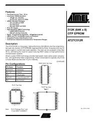
Features• Fast Read Access Time – 70 ns• 5-volt Only Reprogramming• Sector Program Operation– Single Cycle Reprogram (Erase and Program)– 512 Sectors (128 Bytes/Sector)– Internal Address and Data Latches for 128 Bytes• Internal Program Control and Timer• Hardware and Software Data Protection• FastSectorProgramCycleTime–10ms• DATA Polling for End of Program Detection• Low Power Dissipation– 50mAActiveCurrent–100µA CMOS Standby Current• Typical Endurance > 10,000 Cycles• Single 5V ± 10% Supply• CMOS and TTL Compatible Inputs and Outputs• Commercial and Industrial Temperature RangesDescription512K (64K x 8)5-volt Only<strong>Flash</strong> Memory<strong>AT29C512</strong>The <strong>AT29C512</strong> is a 5-volt only in-system <strong>Flash</strong> programmable and erasable read onlymemory (PEROM). Its 512K of memory is organized as 65,536 words by 8 bits. Manufacturedwith Atmel’s advanced nonvolatile CMOS technology, the device offersaccess times to 70 ns with power dissipation of just 275 mW over the commercial temperaturerange. When the device is deselected, the CMOS standby current is lessthan 100 µA. The device endurance is such that any sector can typically be written toin excess of 10,000 times.Pin ConfigurationsDIP Top ViewPin NameA0 - A15CEOEWEI/O0 - I/O7NCFunctionAddressesChip EnableOutput EnableWrite EnableData Inputs/OutputsNo ConnectTSOP Top ViewType 1NCNCA15A12A7A6A5A4A3A2A1A0I/O0I/O1I/O2GND1234567891011121314151632313029282726252423222120191817VCCWENCA14A13A8A9A11OEA10CEI/O7I/O6I/O5I/O4I/O3A11A9A8A13A14NCWEVCCNCNCA15A12A7A6A5A41234567891011121314151632313029282726252423222120191817OEA10CEI/O7I/O6I/O5I/O4I/O3GNDI/O2I/O1I/O0A0A1A2A3A7A6A5A4A3A2A1A0I/O0PLCC Top View5678910111213A12A15NCNCVCCWENC432132313014151617181920I/O1I/O2GNDI/O3I/O4I/O5I/O6292827262524232221A14A13A8A9A11OEA10CEI/O7Rev. 0456E–FLASH–5/021
To allow for simple in-system reprogrammability, the <strong>AT29C512</strong> does not require high inputvoltages for programming. Five-volt-only commands determine the operation of the device.Reading data out of the device is similar to reading from an <strong>EPROM</strong>. Reprogramming the<strong>AT29C512</strong> is performed on a sector basis; 128 bytes of data are loaded into the device andthen simultaneously programmed.During a reprogram cycle, the address locations and 128 bytes of data are internally latched,freeing the address and data bus for other operations. Following the initiation of a programcycle, the device will automatically erase the sector and then program the latched data usingan internal control timer. The end of a program cycle can be detected by DATA polling of I/O7.Once the end of a program cycle has been detected, a new access for a read or program canbegin.Block DiagramDeviceOperationREAD: The<strong>AT29C512</strong>isaccessedlikean<strong>EPROM</strong>.WhenCEand OE are low and WE ishigh, the data stored at the memory location determined by the address pins is asserted onthe outputs. The outputs are put in the high impedance state whenever CE or OE is high. Thisdual-line control gives designers flexibility in preventing bus contention.BYTE LOAD: Byte loads are used to enter the 128 bytes of a sector to be programmed orthe software codes for data protection. A byte load is performed by applying a low pulse on theWE or CE input with CE or WE low (respectively) and OE high. The address is latched on thefalling edge of CE or WE, whichever occurs last. The data is latched by the first rising edge ofCE or WE.PROGRAM: The device is reprogrammed on a sector basis. If a byte of data within a sectoris to be changed, data for the entire sector must be loaded into the device. Any byte that is notloaded during the programming of its sector will be indeterminate. Once the bytes of a sectorare loaded into the device, they are simultaneously programmed during the internal programmingperiod. After the first data byte has been loaded into the device, successive bytes areentered in the same manner. Each new byte to be programmed must have its high-to-low transitionon WE (or CE) within 150 µs of the low-to-high transition of WE (or CE) of the precedingbyte. If a high-to-low transition is not detected within 150 µs of the last low-to-high transition,the load period will end and the internal programming period will start. A7 to A15 specify thesector address. The sector address must be valid during each high-to-low transition of WE (orCE). A0 to A6 specify the byte address within the sector. The bytes may be loaded in anyorder; sequential loading is not required. Once a programming operation has been initiated,and for the duration of t WC , a read operation will effectively be a polling operation.2 <strong>AT29C512</strong>0456E–FLASH–5/02
<strong>AT29C512</strong>SOFTWARE DATA PROTECTION: A software controlled data protection feature is availableon the <strong>AT29C512</strong>. Once the software protection is enabled a software algorithm must beissued to the device before a program may be performed. The software protection feature maybe enabled or disabled by the user; when shipped from Atmel, the software data protectionfeature is disabled. To enable the software data protection, a series of three program commandsto specific addresses with specific data must be performed. After the software dataprotection is enabled the same three program commands must begin each program cycle inorder for the programs to occur. All software program commands must obey the sector programtiming specifications. Once set, the software data protection feature remains activeunless its disable command is issued. Power transitions will not reset the software data protectionfeature; however, the software feature will guard against inadvertent program cyclesduring power transitions.Once set, software data protection will remain active unless the disable command sequence isissued.After setting SDP, any attempt to write to the device without the 3-byte command sequencewill start the internal write timers. No data will be written to the device; however, for the durationof t WC , a read operation will effectively be a polling operation.After the software data protection’s 3-byte command code is given, a byte load is performedby applying a low pulse on the WE or CE input with CE or WE low (respectively) and OE high.The address is latched on the falling edge of CE or WE, whichever occurs last. The data islatched by the first rising edge of CE or WE. The 128 bytes of data must be loaded into eachsector by the same procedure as outlined in the program section under device operation.HARDWARE DATA PROTECTION: Hardware features protect against inadvertent programsto the <strong>AT29C512</strong> in the following ways: (a) V CC sense – if V CC is below 3.8V (typical),the program function is inhibited; (b) V CC power on delay – once V CC has reached the V CCsense level, the device will automatically time out 5 ms (typical) before programming; (c) Programinhibit – holding any one of OE low, CE high or WE high inhibits program cycles; and (d)Noise filter – pulses of less than 15 ns (typical) on the WE or CE inputs will not initiate a programcycle.PRODUCT IDENTIFICATION: The product identification mode identifies the device andmanufacturer as Atmel. It may be accessed by hardware or software operation. The hardwareoperation mode can be used by an external programmer to identify the correct programmingalgorithm for the Atmel product. In addition, users may wish to use the software product identificationmode to identify the part (i.e., using the device code), and have the system softwareuse the appropriate sector size for program operations. In this manner, the user can have acommon board design for 256K to 4-megabit densities and, with each density’s sector size ina memory map, have the system software apply the appropriate sector size.For details, see Operating Modes (for hardware operation) or Software Product Identification.The manufacturer and device code is the same for both modes.0456E–FLASH–5/023
Absolute Maximum Ratings*DATA POLLING: The <strong>AT29C512</strong> features DATA polling to indicate the end of a programcycle. During a program cycle an attempted read of the last byte loaded will result in the complementof the loaded data on I/O7. Once the program cycle has been completed, true data isvalid on all outputs and the next cycle may begin. DATA polling may begin at any time duringthe program cycle.TOGGLE BIT: In addition to DATA polling the <strong>AT29C512</strong> provides another method for determiningthe end of a program or erase cycle. During a program or erase operation, successiveattempts to read data from the device will result in I/O6 toggling between one and zero. Oncethe program cycle has completed, I/O6 will stop toggling and valid data will be read. Examiningthe toggle bit may begin at any time during a program cycle.OPTIONAL CHIP ERASE MODE: The entire device can be erased by using a 6-byte softwarecode. Please see Software Chip Erase application note for details.Temperature Under Bias................................ -55°C to+125°CStorage Temperature ..................................... -65°C to+150°CAll Input Voltages(including NC Pins)with Respect to Ground ...................................-0.6V to +6.25VAll Output Voltageswith Respect to Ground .............................-0.6V to V CC +0.6V*NOTICE: Stresses beyond those listed under “AbsoluteMaximum Ratings” may cause permanent damageto the device. This is a stress rating only andfunctional operation of the device at these or anyother conditions beyond those indicated in theoperational sections of this specification is notimplied. Exposure to absolute maximum ratingconditions for extended periods may affectdevice reliability.Voltage on OEwith Respect to Ground ...................................-0.6V to +13.5V4 <strong>AT29C512</strong>0456E–FLASH–5/02
<strong>AT29C512</strong>DC and AC Operating RangeOperatingTemperature (Case)Notes: 1. X can be V IL or V IH .2. Refer to AC Programming Waveforms.3. V H = 12.0V ± 0.5V.4. Manufacturer Code: 1F, Device Code: 5D.5. See details under Software Product Identification Entry/Exit.<strong>AT29C512</strong>-70 <strong>AT29C512</strong>-90 <strong>AT29C512</strong>-12 <strong>AT29C512</strong>-15Com. 0°C -70°C 0°C -70°C 0°C -70°C 0°C -70°CInd. -40°C -85°C -40°C -85°C -40°C -85°CV CC Power Supply 5V ± 5% 5V ± 10% 5V ± 10% 5V ± 10%Note:Operating ModesNot recommended for New Designs.Mode CE OE WE Ai I/ORead V IL V IL V IH Ai D OUTProgram (2) V IL V IH V IL Ai D IN5V Chip Erase V IL V IH V IL AiStandby/Write Inhibit V IH X (1) X X High ZProgram Inhibit X X V IHProgram Inhibit X V IL XOutput Disable X V IH X High ZProduct IdentificationHardware V IL V IL V IH A1 - A15 = V IL ,A9=V H , (3) A0 = V IL Manufacturer Code (4)A1-A15 = V IL ,A9=V H , (3) A0 = V IH Device Code (4)Software (5) A0 = V IL Manufacturer Code (4)DC CharacteristicsA0 = V IH Device Code (4)Symbol Parameter Condition Min Max UnitsI LI Input Load Current V IN =0VtoV CC 10 µAI LO Output Leakage Current V I/O =0VtoV CC 10 µAI SB1 V CC Standby Current CMOS CE =V CC -0.3VtoV CC Com. 100 µAInd. 300 µAI SB2 V CC Standby Current TTL CE =2.0VtoV CC 3 mAI CC V CC Active Current f = 5 MHz; I OUT = 0 mA 50 mAV IL Input Low Voltage 0.8 VV IH Input High Voltage 2.0 VV OL Output Low Voltage I OL =2.1mA 0.45 VV OH1 Output High Voltage I OH =-400µA 2.4 VV OH2 Output High Voltage CMOS I OH =-100µA; V CC =4.5V 4.2 V0456E–FLASH–5/025
AC Read CharacteristicsSymbolParameter<strong>AT29C512</strong>-70 <strong>AT29C512</strong>-90 <strong>AT29C512</strong>-12 <strong>AT29C512</strong>-15Min Max Min Max Min Max Min Maxt ACC Address to Output Delay 70 90 120 150 nst CE(1)t OE(2)t DF(3)(4)t OHCE to Output Delay 70 90 120 150 nsOE to Output Delay 0 35 0 40 0 50 0 70 nsCE or OE to Output Float 0 10 0 25 0 30 0 40 nsOutput Hold from OE, CEorAddress, whicheveroccurred first0 0 0 0 nsUnitsNote:Not recommended for New Designs.AC Read Waveforms (1)(2)(3)(4)Notes: 1. CE may be delayed up to t ACC -t CE after the address transition without impact on t ACC .2. OE may be delayed up to t CE -t OE after the falling edge of CE without impact on t CE or by t ACC -t OE after an address changewithout impact on t ACC .3. t DF is specified from OE or CE whichever occurs first (CL = 5 pF).4. This parameter is characterized and is not 100% tested.6 <strong>AT29C512</strong>0456E–FLASH–5/02
<strong>AT29C512</strong>Input Test Waveforms and Measurement Levelt R ,t F
AC Byte Load CharacteristicsSymbol Parameter Min Max Unitst AS ,t OES Address, OE Set-up Time 0 nst AH Address Hold Time 50 nst CS Chip Select Set-up Time 0 nst CH Chip Select Hold Time 0 nst WP Write Pulse Width (WE or CE) 90 nst DS Data Set-up Time 35 nst DH ,t OEH Data, OE Hold Time 0 nst WPH Write Pulse Width High 100 nsAC Byte Load WaveformsWE ControlledOEADDRESSt OEStOEHCEWEt ASt AHt WPt CSt CHt WPHt DSt DHDATA INCE ControlledOEADDRESSt OESt OEHWECEt AS t AHt WPt CSt CHt WPHt DSt DHDATA IN8 <strong>AT29C512</strong>0456E–FLASH–5/02
<strong>AT29C512</strong>Program Cycle CharacteristicsSymbol Parameter Min Max Unitst WC WriteCycleTime 10 mst AS Address Set-up Time 0 nst AH Address Hold Time 50 nst DS Data Set-up Time 35 nst DH Data Hold Time 0 nst WP Write Pulse Width 90 nst BLC Byte Load Cycle Time 150 µst WPH Write Pulse Width High 100 nsProgram Cycle Waveforms (1)(2)(3)Notes: 1. A7 through A15 must specify the sector address during each high-to-low transition of WE (or CE).2. OE must be high when WE and CE arebothlow.3. All bytes that are not loaded within the sector being programmed will be indeterminate.0456E–FLASH–5/029
Software Data Protection Enable Algorithm (1)LOAD DATA AATOADDRESS 5555LOAD DATA 55TOADDRESS 2AAALOAD DATA A0TOADDRESS 5555LOAD DATATOPAGE (128 BYTES) (4)Software Data Protection Disable Algorithm (1)LOAD DATA AATOADDRESS 5555LOAD DATA 55TOADDRESS 2AAALOAD DATA 80TOWRITES ENABLEDADDRESS 5555LOAD DATA AAENTER DATATOPROTECT STATE (2) ADDRESS 5555LOAD DATA 55TOADDRESS 2AAANotes: 1. Data Format: I/O7 - I/O0 (Hex);Address Format: A14 -A0 (Hex).2. Data Protect state will be activated at end of programcycle.3. Data Protect state will be deactivated at end of programperiod.4. 128 bytes of data MUST BE loaded.LOAD DATA 20TOADDRESS 5555LOAD DATATOPAGE (128 BYTES) (4)EXIT DATAPROTECT STATE (3)Software Protected Program Cycle Waveform (1)(2)(3)OE (1)CEWEA0-A6A7-A15 (2)t ASt WPHt WPt AHt DHBYTE ADDRESS5555 2AAA 5555SECTOR ADDRESSt DSt BLCDATA (3) AA 55 A0BYTE 0 BYTE 126 BYTE 127Notes: 1. A7 through A15 must specify the page address during each high-to-low transition of WE (or CE) after the software code hasbeen entered.2. OE must be high when WE and CE arebothlow.3. All bytes that are not loaded within the sector being programmed will be indeterminate.t WC10 <strong>AT29C512</strong>0456E–FLASH–5/02
<strong>AT29C512</strong>Data Polling Characteristics (1)Symbol Parameter Min Typ Max Unitst DH Data Hold Time 10 nst OEH OE Hold Time 10 nst OE OE to Output Delay (2) nst WR Write Recovery Time 0 nsNotes: 1. These parameters are characterized and not 100% tested.2. See t OE spec in AC Read Characteristics.Data Polling WaveformsToggle Bit Characteristics (1)Symbol Parameter Min Typ Max Unitst DH Data Hold Time 10 nst OEH OE Hold Time 10 nst OE OE to Output Delay (2) nst OEHP OE High Pulse 150 nst WR Write Recovery Time 0 nsNotes: 1. These parameters are characterized and not 100% tested.2. See t OE spec in AC Read Characteristics.Toggle Bit Waveforms (1)(2)(3)WECEt OEHOEI/O6 (2) t DHt OEHIGH Zt WRNotes: 1. Toggling either OE or CE or both OE and CE will operate toggle bit.2. Beginning and ending state of I/O6 will vary.3. Any address location may be used but the address should not vary.0456E–FLASH–5/0211
Software Product Identification Entry (1)LOAD DATA AATOADDRESS 5555LOAD DATA 55TOADDRESS 2AAALOAD DATA 90TOADDRESS 5555PAUSE 10 mSSoftware Product Identification Exit (1)ENTER PRODUCTIDENTIFICATIONLOAD DATA AATOADDRESS 5555LOAD DATA 55TOADDRESS 2AAALOAD DATA F0TOADDRESS 5555PAUSE 10 mS EXIT PRODUCTIDENTIFICATIONMODE (4)Notes: 1. Data Format: I/O7 - I/O0 (Hex); Address Format: A14 - A0 (Hex).2. A1 - A15 = V IL . Manufacturer Code is read for A0 = V IL ;DeviceCodeisreadforA0=V IH .3. The device does not remain in identification mode if powered down.4. The device returns to standard operation mode.5. Manufacturer Code is 1F. The Device Code is 5D.12 <strong>AT29C512</strong>0456E–FLASH–5/02
<strong>AT29C512</strong>NORMALIZEDICC1.41.31.21.11.00.90.8-55NORMALIZED SUPPLY CURRENTvs. TEMPERATURE-25 5 35 65 95 125TEMPERATURE (C)NORMALIZEDICC1.11.00.90.80.70NORMALIZED SUPPLY CURRENTvs. ADDRESS FREQUENCYV CC = 5VT = 25C1 2 3 4 5 6 7FREQUENCY (MHz)NORMALIZEDICC1.41.21.00.80.64.50NORMALIZED SUPPLY CURRENTvs. SUPPLY VOLTAGE4.75 5.00 5.25 5.50SUPPLY VOLTAGE (V)0456E–FLASH–5/0213
Ordering Informationt ACC(ns)ActiveI CC (mA)StandbyOrdering Code Package Operation Range70 50 0.1 <strong>AT29C512</strong>-70JC<strong>AT29C512</strong>-70PC<strong>AT29C512</strong>-70TC90 50 0.1 <strong>AT29C512</strong>-90JC<strong>AT29C512</strong>-90PC<strong>AT29C512</strong>-90TC50 0.3 <strong>AT29C512</strong>-90JI<strong>AT29C512</strong>-90PI<strong>AT29C512</strong>-90TI120 50 0.1 <strong>AT29C512</strong>-12JC<strong>AT29C512</strong>-12PC<strong>AT29C512</strong>-12TC50 0.3 <strong>AT29C512</strong>-12JI<strong>AT29C512</strong>-12PI<strong>AT29C512</strong>-12TI150 50 0.1 <strong>AT29C512</strong>-15JC<strong>AT29C512</strong>-15PC<strong>AT29C512</strong>-15TC50 0.3 <strong>AT29C512</strong>-15JI<strong>AT29C512</strong>-15PI<strong>AT29C512</strong>-15TI32J32P632T32J32P632T32J32P632T32J32P632T32J32P632T32J32P632T32J32P632TCommercial(0° to 70°C)Commercial(0° to 70°C)Industrial(-40° to 85°C)Commercial(0° to 70°C)Industrial(-40° to 85°C)Commercial(0° to 70°C)Industrial(-40° to 85°C)Note:Not recommended for New Designs.Package Type32J32P632T32-lead, Plastic J-leaded Chip Carrier (PLCC)32-pin, 0.600" Wide, Plastic Dual Inline Package (PDIP)32-lead, Thin Small Outline Package (TSOP)14 <strong>AT29C512</strong>0456E–FLASH–5/02
<strong>AT29C512</strong>Packaging Information32J – PLCC1.14(0.045) X 45˚ PIN NO. 1IDENTIFIER1.14(0.045) X 45˚0.318(0.0125)0.191(0.0075)BE1EB1E2eD1DAA2A10.51(0.020)MAX45˚ MAX (3X)COMMON DIMENSIONS(Unit of Measure = mm)Notes:D21. This package conforms to JEDEC reference MS-016, Variation AE.2. Dimensions D1 and E1 do not include mold protrusion.Allowable protrusion is .010"(0.254 mm) per side. Dimension D1and E1 include mold mismatch and are measured at the extremematerial condition at the upper or lower parting line.3. Lead coplanarity is 0.004" (0.102 mm) maximum.SYMBOL MIN NOM MAX NOTEA 3.175 – 3.556A1 1.524 – 2.413A2 0.381 – –D 12.319 – 12.573D1 11.354 – 11.506 Note 2D2 9.906 – 10.922E 14.859 – 15.113E1 13.894 – 14.046 Note 2E2 12.471 – 13.487B 0.660 – 0.813B1 0.330 – 0.533e1.270 TYP10/04/01R2325 Orchard ParkwaySan Jose, CA 95131TITLE32J, 32-lead, Plastic J-leaded Chip Carrier (PLCC)DRAWING NO.32JREV.B0456E–FLASH–5/0215
32P6 – PDIPDPIN1E1ASEATING PLANELeB1BA1Note:CEeB0º ~ 15º1. Dimensions D and E1 do not include mold <strong>Flash</strong> or Protrusion.Mold <strong>Flash</strong> or Protrusion shall not exceed 0.25 mm (0.010").REFCOMMON DIMENSIONS(Unit of Measure = mm)SYMBOL MIN NOM MAX NOTEA – – 4.826A1 0.381 – –D 41.783 – 42.291 Note 1E 15.240 – 15.875E1 13.462 – 13.970 Note 1B 0.356 – 0.559B1 1.041 – 1.651L 3.048 – 3.556C 0.203 – 0.381eB 15.494 – 17.526e2.540 TYP09/28/01R2325 Orchard ParkwaySan Jose, CA 95131TITLE32P6, 32-lead (0.600"/15.24 mm Wide) Plastic DualInline Package (PDIP)DRAWING NO.32P6REV.B16 <strong>AT29C512</strong>0456E–FLASH–5/02
<strong>AT29C512</strong>32T – TSOPPIN 10º ~ 8ºcPin 1 IdentifierD1DLebL1EA2ASEATING PLANEGAGE PLANEA1COMMON DIMENSIONS(Unit of Measure = mm)Notes:1. This package conforms to JEDEC reference MO-142, Variation BD.2. Dimensions D1 and E do not include mold protrusion. Allowableprotrusion on E is 0.15 mm per side and on D1 is 0.25 mm per side.3. Lead coplanarity is 0.10 mm maximum.SYMBOL MIN NOM MAX NOTEA – – 1.20A1 0.05 – 0.15A2 0.95 1.00 1.05D 19.80 20.00 20.20D1 18.30 18.40 18.50 Note 2E 7.90 8.00 8.10 Note 2L 0.50 0.60 0.70L10.25 BASICb 0.17 0.22 0.27c 0.10 – 0.21e0.50 BASIC10/18/01R2325 Orchard ParkwaySan Jose, CA 95131TITLE32T, 32-lead (8 x 20 mm Package) Plastic Thin Small OutlinePackage, Type I (TSOP)DRAWING NO.32TREV.B0456E–FLASH–5/0217
Atmel HeadquartersCorporate Headquarters2325 Orchard ParkwaySan Jose, CA 95131TEL 1(408) 441-0311FAX 1(408) 487-2600EuropeAtmel SarlRoute des Arsenaux 41Case Postale 80CH-1705 FribourgSwitzerlandTEL (41) 26-426-5555FAX (41) 26-426-5500AsiaRoom 1219Chinachem Golden Plaza77 Mody Road TsimshatsuiEast KowloonHong KongTEL (852) 2721-9778FAX (852) 2722-1369Japan9F, Tonetsu Shinkawa Bldg.1-24-8 ShinkawaChuo-ku, Tokyo 104-0033JapanTEL (81) 3-3523-3551FAX (81) 3-3523-7581Atmel OperationsMemory2325 Orchard ParkwaySan Jose, CA 95131TEL 1(408) 441-0311FAX 1(408) 436-4314Microcontrollers2325 Orchard ParkwaySan Jose, CA 95131TEL 1(408) 441-0311FAX 1(408) 436-4314La ChantrerieBP 7060244306 Nantes Cedex 3, FranceTEL (33) 2-40-18-18-18FAX (33) 2-40-18-19-60ASIC/ASSP/Smart CardsZone Industrielle13106 Rousset Cedex, FranceTEL (33) 4-42-53-60-00FAX (33) 4-42-53-60-011150 East Cheyenne Mtn. Blvd.Colorado Springs, CO 80906TEL 1(719) 576-3300FAX 1(719) 540-1759Scottish Enterprise Technology ParkMaxwell BuildingEast Kilbride G75 0QR, ScotlandTEL (44) 1355-803-000FAX (44) 1355-242-743RF/AutomotiveTheresienstrasse 2Postfach 353574025 Heilbronn, GermanyTEL (49) 71-31-67-0FAX (49) 71-31-67-23401150 East Cheyenne Mtn. Blvd.Colorado Springs, CO 80906TEL 1(719) 576-3300FAX 1(719) 540-1759Biometrics/Imaging/Hi-Rel MPU/High Speed Converters/RF DatacomAvenue de RochepleineBP 12338521 Saint-Egreve Cedex, FranceTEL (33) 4-76-58-30-00FAX (33) 4-76-58-34-80e-mailliterature@atmel.comWeb Sitehttp://www.atmel.com© Atmel Corporation 2002.Atmel Corporation makes no warranty for the use of its products, other than those expressly contained in the Company’s standard warrantywhichisdetailedinAtmel’s Terms and Conditions located on the Company’s web site. The Company assumes no responsibility for any errorswhich may appear in this document, reserves the right to change devices or specifications detailed herein at any time without notice, and doesnot make any commitment to update the information contained herein. No licenses to patents or other intellectual property of Atmel are grantedby the Company in connection with the sale of Atmel products, expressly or by implication. Atmel’s products are not authorized for use as criticalcomponents in life support devices or systems.ATMEL ® is the registered trademark of Atmel.Other terms and product names may be the trademarks of others.Printed on recycled paper.0456E–FLASH–5/02/xM