GL6962/GL6962A - abov.co.kr
GL6962/GL6962A - abov.co.kr
GL6962/GL6962A - abov.co.kr

Create successful ePaper yourself
Turn your PDF publications into a flip-book with our unique Google optimized e-Paper software.
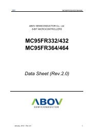
<strong>GL6962</strong>/<strong>GL6962</strong>A<strong>GL6962</strong>/<strong>GL6962</strong>ALow Voltage Universal Speech NetworkDescriptionThe <strong>GL6962</strong> and <strong>GL6962</strong>A are bipolar integratedcircuits that perform all speech and line interfacefunctions required in fully electronic telephone sets.They perform electronic switching between dialingand speech. The ICs operate at line voltage downto 1.6V DC (with reduced performance) tofacilitate the use of more telephone sets <strong>co</strong>nnectedin parallel.Features● Low DC line voltage: operates down to 1.6V(excluding polarity guard)● Voltage regulator with adjustable staticresistance● Provides a supply for external circuits● Symmetrical high-impedance inputs (64k) fordynamic, magnetic or piezo-electric microphones● Asymmetrical high-impedance inputs(32k)for electric microphones● DTMF signal input with <strong>co</strong>nfidence tone● MUTE input for pulse or DTMF dialing(<strong>GL6962</strong>)● MUTE input for pulse or DTMF dialing(<strong>GL6962</strong>A)● Receiving amplifier for dynamic, magnetic orpiezo-electric earpieces.● Large gain setting ranges on microphone andearpiece amplifiers.● Line loss <strong>co</strong>mpensation (line current dependent)for microphone and earpiece amplifiers● Gain <strong>co</strong>ntrol curve adaptable to exchange supply● DC line voltage adjustment facility● Packaged in 16 DIP/SOP.PIN Configuration(TOP View)LN 161SLPETGA1 215 AGCTGA2 314QR 413<strong>GL6962</strong>RGA 512MIC- 611MIC+ 107I ref89REGV CCMUTEDTMFIRV EE* Pin 12 is active LOW(MUTE) for <strong>GL6962</strong>A- 1 -
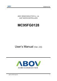
<strong>GL6962</strong>/<strong>GL6962</strong>ABlock DiagramV CC13LN1RGCIR 10-54RGAQR+MICMIC-76+TGCRM-2TGA1DTMF11dB++3TGA2(1)MUTE12MUTECONTROLRMSUPPLY&REFERENCECURRENTREFERENCERGC TGCΣCURRENTCONTROLLOWVOLTAGECIRCUIT9V EE8I ref15AGC14REG16SLPE* Pin 12 is active LOW ( MUTE ) for <strong>GL6962</strong>A.- 2 -
<strong>GL6962</strong>/<strong>GL6962</strong>APin DescriptionPIN NUMBER SYMBOL DESCRIPTION1 LN Positive line terminal2 TGA1 Gain adjustment: transmitting amplifier3 TGA2 Gain adjustment: transmitting amplifier4 QR Non-inverting output: receiving amplifier5 RGA Gain adjustment: receiving amplifier6 MIC- Inverting microphone input7 MIC+ Non-Inverting microphone input8 I ref Current stabilizer9 V EE Negative line terminal10 IR Receiving amplifier input11 DTMF Dual-tone multi-frequency input12 MUTE Mute input (1)13 V CC Positive de<strong>co</strong>upling14 REG Voltage regulator de<strong>co</strong>upling15 AGC Automatic gain <strong>co</strong>ntrol input16 SLPE Slope (DC resistance) adjustment.(1) Pin 12 is active LOW (MUTE ) for <strong>GL6962</strong>A.- 3 -
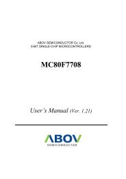
<strong>GL6962</strong>/<strong>GL6962</strong>ATest CircuitI lineR1162013100 F+R L600V OR4100kC4100pFC71 nF1045QRIRRGALN V CCDTMF<strong>GL6962</strong>AMUTE1112C1 F10 to140mAV i76MIC+MIC-SLPETGA1TGA2REGAGCI refV EE+10 F1623141589ViR920C6100pFR768kC81 nFC34.7 F +R6R5For measuring gain from MIC+ and MIC-, the MUTE input should be LOW or open-circuit.For measuring the DTMF input, the MUTE input should be HIGH.Inputs not being tested should be open-circuit.Fig. 1 Test circuit for defining <strong>GL6962</strong> voltage gain of MIC+, MIC- and DTMF inputs.(Voltage gain is defined as G V = 20log |V o /V i |- 8 -
<strong>GL6962</strong>/<strong>GL6962</strong>AI lineR1162013100 F+R L600V O LN V CCV EE10IR4QRR4 C4DTMF11100k 100pF5RGAC7<strong>GL6962</strong>A121 nFMUTEC1 F10 to140mAV i76MIC+MIC-SLPETGA1TGA2REGAGCI ref+10 F1623141589R920C6100pFR768kC81 nFC34.7 F +R6R5For measuring gain from MIC+ and MIC-, the MUTE input should be HIGH.For measuring the DTMF input, the MUTE input should be LOW or open-circuit.Inputs not being tested should be open-circuit.Fig. 2 Test circuit for defining <strong>GL6962</strong>A voltage gain of MIC+, MIC- and DTMF inputs.(Voltage gain is defined as G V = 20log |V o /V i |- 9 -
<strong>GL6962</strong>/<strong>GL6962</strong>AI line+R1100 F60010V O+ 10µFIR162013Z L1110 to140mAR4100kC2C4100pFC71 nFV i4576QRRGAMIC+MIC-SLPE16TGA12LN V CCDTMF<strong>GL6962</strong>TGA2 REG3 14AGC15I ref8MUTEV EE912+C1 FR920C6100pFR768kC81 nFC34.7 F +R6R5Fig. 3 Test circuit for defining <strong>GL6962</strong> voltage gain of receiving amplifier.(Voltage gain is defined as G V = 20log |V o /V i |- 10 -
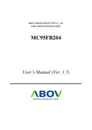
<strong>GL6962</strong>/<strong>GL6962</strong>AApplication CircuitR1R 1013µΩ12VR2130KΩC2C5100nF10IR162013C1100µF+TelephoneLineR4R33.92kC4100pFC71 nF45QRRGALN V CCDTMF<strong>GL6962</strong>(1) MUTE1112from dialand<strong>co</strong>ntrol circuit7MIC+6MIC-SLPETGA1TGA2REGAGCI refV EER816C62R73141589390ΩZ balR920C81 nFR VA (R 16-14 )C34.7 F+R6R5(1) Pin 12 is active LOW ( MUTE ) for <strong>GL6962</strong>A.Fig. 5 Typical application of <strong>GL6962</strong>, shown there with piezo-electric earpiece and DTMF dialing.(The diode bridge, the zener diode and R10 limit current into, and the voltage across, the circuitduring line transients. A different protection requirement is required for pulse dialing or registerrecall.)- 12 -