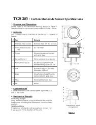
"Quadruple Differential Comparators" - Meditronik
"Quadruple Differential Comparators" - Meditronik
"Quadruple Differential Comparators" - Meditronik

You also want an ePaper? Increase the reach of your titles
YUMPU automatically turns print PDFs into web optimized ePapers that Google loves.
TLC374, TLC374Q, TLC374YLinCMOS QUADRUPLE DIFFERENTIAL COMPARATORSSLCS118C – NOVEMBER 1983 – REVISED MARCH 1999electrical characteristics at specified free-air temperature, V DD = 5 V, T A = 25°C (unless otherwisenoted)PARAMETERTEST CONDITIONSTLC374YMIN TYP MAXVIO Input offset voltage VIC = VICRmin, See Note 4 1 5 mVIIO Input offset current 1 pAIIB Input bias current 5 pAVICR Common-mode input voltage range 0 to VDD –1 VIOH High-level output current VID = 1 V, VOH = 5 V 0.1 nAVOL Low-level output voltage VID = – 1 V, IOL = 4 mA 150 400 mVIOL Low-level output current VID = – 1 V, VOL = 1.5 mV 6 16 mAIDD Supply current (four comparators) VID =1 V, No load 300 600 µANOTE 4: The offset voltage limits given are the maximum values required to drive the output above 4 V or below 400 mV with a 10-kΩ resistorbetween the output and VDD. They can be verified by applying the limit value to the input and checking for the appropriate output state.switching characteristics, V DD = 5 V, T A = 25°CUNITPARAMETERResponse timeTEST CONDITIONSTLC374YMIN TYP MAXRL L connected to 5 V through 5.1 kΩ, 100-mV input step with 5-mV overdrive 650CL = 15 pF †, See Note 5 TTL-level input step 200† CL includes probe and jig capacitance.NOTE 4: The response time specified is the interval between the input step function and the instant when the output crosses 1.4 V.UNITns6 POST OFFICE BOX 655303 • DALLAS, TEXAS 75265
TLC374, TLC374Q, TLC374YLinCMOS QUADRUPLE DIFFERENTIAL COMPARATORSPARAMETER MEASUREMENT INFORMATIONSLCS118C – NOVEMBER 1983 – REVISED MARCH 1999The digital output stage of the TLC374 can be damaged if it is held in the linear region of the transfer curve.Conventional operational amplifier/comparator testing incorporates the use of a servo loop that is designed to forcethe device output to a level within this linear region. Since the servo-loop method of testing cannot be used, thefollowing alternative for measuring parameters such as input offset voltage, common-mode rejection, etc., areoffered.To verify that the input offset voltage falls within the limits specified, the limit value is applied to the input as shownin Figure 1(a). With the noninverting input positive with respect to the inverting input, the output should be high. Withthe input polarity reversed, the output should be low.A similar test can be made to verify the input offset voltage at the common-mode extremes. The supply voltages canbe slewed as shown in Figure 1(b) for the V ICR test, rather than changing the input voltages, to provide greateraccuracy.A close approximation of the input offset voltage can be obtained by using a binary search method to vary thedifferential input voltage while monitoring the output state. When the applied input voltage differential is equal, butopposite in polarity to the input offset voltage, the output changes state.5 V1 V5.1 kΩ5.1 kΩApplied VIOLimitVOApplied VIOLimitVO–4 V(a) VIO WITH VIC = 0(b) VIO WITH VIC = 4 VFigure 1. Method for Verifying That Input Offset Voltage is Within Specified LimitsPOST OFFICE BOX 655303 • DALLAS, TEXAS 752657
TLC374, TLC374Q, TLC374YLinCMOS QUADRUPLE DIFFERENTIAL COMPARATORSSLCS118C – NOVEMBER 1983 – REVISED MARCH 1999PARAMETER MEASUREMENT INFORMATIONFigure 2 illustrates a practical circuit for direct dc measurement of input offset voltage that does not bias thecomparator into the linear region. The circuit consists of a switching-mode servo loop in which U1a generates atriangular waveform of approximately 20-mV amplitude. U1b acts as a buffer with C2 and R4 removing any residualdc offset. The signal is then applied to the inverting input of the comparator under test, while the noninverting inputis driven by the output of the integrator formed by U1c through the voltage divider formed by R9 and R10. The loopreaches a stable operating point when the output of the comparator under test has a duty cycle of exactly 50%, whichcan only occur when the incoming triangle wave is sliced symmetrically or when the voltage at the noninverting inputexactly equals the input offset voltage.Voltage divider R9 and R10 provide a step up of the input offset voltage by a factor of 100 to make measurementeasier. The values of R5, R8, R9, and R10 can significantly influence the accuracy of the reading; therefore, it issuggested that their tolerance level be 1% or lower.Measuring the extremely low values of input current requires isolation from all other sources of leakage current andcompensation for the leakage of the test socket and board. With a good picoammeter, the socket and board leakagecan be measured with no device in the socket. Subsequently, this open-socket leakage value can be subtracted fromthe measurement obtained with a device in the socket to obtain the actual input current of the device.VDDR51.8 kΩ, 1%C30.68 µFU1b1/4 TLC274CN+–R1240 kΩBufferC21 µFR447 kΩDUTU1aC1+–1/4 TLC274CNTriangle0.1 µF GeneratorR10R2100 Ω, 1%R3 10 kΩ100 kΩR65.1 kΩR81.8 kΩ, 1%R910 kΩ, 1%R71 MΩU1c1/4 TLC274CN–+C40.1 µFIntegratorVIO(X100)Figure 2. Test Circuit for Input Offset Voltage Measurement8 POST OFFICE BOX 655303 • DALLAS, TEXAS 75265
TLC374, TLC374Q, TLC374YLinCMOS QUADRUPLE DIFFERENTIAL COMPARATORSPARAMETER MEASUREMENT INFORMATIONSLCS118C – NOVEMBER 1983 – REVISED MARCH 1999Response time is defined as the interval between the application of an input step function and the instant when theoutput reaches 50% of its maximum value. Response time, low-to-high-level output, is measured from the trailingedge of the input pulse. Response-time measurement at low input signal levels can be greatly affected by the inputoffset voltage. The offset voltage should be balanced by the adjustment at the inverting input (as shown in Figure 3)so that the circuit is just at the transition point. Then a low signal, for example, 105-mV or 5-mV overdrive, causesthe output to change state.VDD5.1 kΩ1 µF1 VInputOffset Voltage 10 ΩCompensation 10 TurnAdjustment–1 VPulse Generator1 kΩ50 Ω0.1 µFOUTCL(see Note A)TEST CIRCUITOverdriveInputInput100 mVOverdrive100 mVLow-to-High-Level OutputtPLH50%tr90%10%High-to-Low-Level Output90%50%10%tftPLHVOLTAGE WAVEFORMSNOTE A: CL includes probe and jig capacitance.Figure 3. Response, Rise, and Fall Times Test Circuit and Voltage WaveformsPOST OFFICE BOX 655303 • DALLAS, TEXAS 752659
TLC374, TLC374Q, TLC374YLinCMOS QUADRUPLE DIFFERENTIAL COMPARATORSSLCS118C – NOVEMBER 1983 – REVISED MARCH 1999LinCMOS processPRINCIPLES OF OPERATIONLinCMOS process is a linear polysilicon-gate complimentary-MOS process. Primarily designed for singlesupplyapplications, LinCMOS products facilitate the design of a wide range of high-performance analogfunctions from operational amplifiers to complex mixed-mode converters.While digital designers are experienced with CMOS, MOS technologies are relatively new for analog designers.This short guide is intended to answer the most frequently asked questions related to the quality and reliabilityof LinCMOS products. Further questions should be directed to the nearest TI field sales office.electrostatic dischargeCMOS circuits are prone to gate oxide breakdown when exposed to high voltages even if the exposure is onlyfor very short periods of time. Electrostatic discharge (ESD) is one of the most common causes of damage toCMOS devices. It can occur when a device is handled without proper consideration for environmentalelectrostatic charges, e.g. during board assembly. If a circuit in which one amplifier from a dual operationalamplifier is being used and the unused pins are left open, high voltages tends to develop. If there is no provisionfor ESD protection, these voltages may eventually punch through the gate oxide and cause the device to fail.To prevent voltage buildup, each pin is protected by internal circuitry.Standard ESD-protection circuits safely shunt the ESD current by providing a mechanism whereby one or moretransistors break down at voltages higher than normal operating voltages but lower than the breakdown voltageof the input gate. This type of protection scheme is limited by leakage currents which flow through the shuntingtransistors during normal operation after an ESD voltage has occurred. Although these currents are small, onthe order of tens of nanoamps, CMOS amplifiers are often specified to draw input currents as low as tens ofpicoamps.To overcome this limitation, TI design engineers developed the patented ESD-protection circuit shown inFigure 4. This circuit can withstand several successive 1-kV ESD pulses, while reducing or eliminating leakagecurrents that may be drawn through the input pins. A more detailed discussion of the operation of TI’sESD-protection circuit is presented on the next page.All input an output pins of LinCMOS and Advanced LinCMOS products have associated ESD-protectioncircuitry that undergoes qualification testing to withstand 1000 V discharged from a 100-pF capacitor througha 1500-Ω resistor (human body model) and 200 V from a 100-pF capacitor with no current-limiting resistor(charged device model). These tests simulate both operator and machine handling of devices during normaltest and assembly operations.InputR1VDDTo Protected CircuitR2Q1Q2D1D2D3VSSFigure 4. LinCMOS ESD-Protection Schematic10 POST OFFICE BOX 655303 • DALLAS, TEXAS 75265
TLC374, TLC374Q, TLC374YLinCMOS QUADRUPLE DIFFERENTIAL COMPARATORSPRINCIPLES OF OPERATIONSLCS118C – NOVEMBER 1983 – REVISED MARCH 1999Input protection circuit operationTexas Instruments patented protection circuitry allows for both positive- and negative-going ESD transients.These transients are characterized by extremely fast rise times and usually low energies, and can occur bothwhen the device has all pins open and when it is installed in a circuit.positive ESD transientsInitial positive charged energy is shunted through Q1 to V SS . Q1 turns on when the voltage at the input risesabove the voltage on V DD by a value equal to the V EB of Q1. The base current increases through R2 with inputcurrent as Q1 saturates. The base current through R2 as Q1 saturates forces the voltage at the drain and gateof Q2 to exceed its threshold level (V T ∼ 22 to 26 V) and turn on Q2. The shunted input current through Q1 toV SS is now shunted through the n-channel enhancement-type MOSFET Q2 to V SS . If the voltage on the inputpin continues to rise, the breakdown voltage of d3 is exceeded and all remaining energy is dissipated in R1 andD3. The breakdown voltage of D3 is designed to be 24 V to 27 V, which is well below the gate oxide voltage ofthe circuit to be protected.negative ESD transientsThe negative charged ESD transients are shunted directly through D1. Additional energy is dissipated in R1and D2 as D2 becomes forward-biased. The voltage seen by the protected circuit is –0.3 V to –1 V (the forwardvoltage of D1 and D2).circuit-design considerationsLinCMOS products are being used in actual circuits environments that have input voltages that exceed therecommended common-mode input voltage range and activate the input protection circuit. Even under normaloperation, these conditions occur during circuit power up or power down, and in many cases, when the deviceis being used for a signal conditioning function. The input voltages can exceed V ICR and not damage the deviceonly if the inputs are current limited. The recommended current limit shown on most product data sheets is±5 mA. Figures 5 and 6 show typical characteristics for input voltage vs input current.Normal operation and correct output state can be expected even when the input voltage exceeds the positivesupply voltage. The input current should be externally limited even through internal positive current limiting isachieved in the input protection circuit by the action of Q1. When Q1 is on, it saturates and limits the currentto approximately 5-mA collector current by design. When saturated, Q1 base current increases with inputcurrent. This current is forced into the V DD pin and into the device I DD or the V DD supply through R2 producingthe current limiting effects shown in Figure 5. This internal limiting lasts only as long as the input voltage is belowthe V T of Q2.When the input voltage exceeds the negative supply voltage, normal operation is affected and output voltagestates may not be correct. Also, the isolation between channels of multiple devices (duals and quads) can beseverely affected. External current limiting must be used since this current is directly shunted by D1 and D2,and no internal limiting is achieved. If normal output voltage states are required, an external input voltage clampis required (see Figure 7).POST OFFICE BOX 655303 • DALLAS, TEXAS 7526511
TLC374, TLC374Q, TLC374YLinCMOS QUADRUPLE DIFFERENTIAL COMPARATORSSLCS118C – NOVEMBER 1983 – REVISED MARCH 1999PRINCIPLES OF OPERATIONII– Input Current – mA87654321TA = 25°CINPUT CURRENTvsINPUT VOLTAGE †0VDD VDD +4 VDD +8 VDD +12VI – Input Voltage – V† The dashed line identifies an area of operation where somedegradation of parametric performance may be experienced.Figure 5II– Input Current – mA10987654321TA = 25°CINPUT CURRENTvsINPUT VOLTAGE †0VDD– 0.3 VDD – 0.5 VDD – 0.7 VDD – 0.9VI – Input Voltage – V† The dashed line identifies an area of operation where somedegradation of parametric performance may be experienced.Figure 6VDDVIRLSee Note AVREF+–1/4TLC374RLPositive Voltage Input Current Limit:+VI – VDD – 0.3 VRI =5 mANegative Voltage Input Current Limit:–VI – VDD – (0.3 V)RI =5 mANOTE A: If the correct output state is required when the negative input exceeds VSS, a Schotty clamp is required.Figure 7. Typical Input Current-Limiting Configuration for a LinCMOS Comparator12 POST OFFICE BOX 655303 • DALLAS, TEXAS 75265
TLC374, TLC374Q, TLC374YLinCMOS QUADRUPLE DIFFERENTIAL COMPARATORSSLCS118C – NOVEMBER 1983 – REVISED MARCH 1999D (R-PDSO-G**)14 PIN SHOWNMECHANICAL INFORMATIONPLASTIC SMALL-OUTLINE PACKAGE0.050 (1,27)0.020 (0,51)0.014 (0,35)0.010 (0,25)M1480.157 (4,00)0.150 (3,81)0.244 (6,20)0.228 (5,80)0.008 (0,20) NOMGage Plane1A70°–8°0.010 (0,25)0.044 (1,12)0.016 (0,40)0.069 (1,75) MAX0.010 (0,25)0.004 (0,10)Seating Plane0.004 (0,10)DIMPINS **81416A MAX0.197(5,00)0.344(8,75)0.394(10,00)A MIN0.189(4,80)0.337(8,55)0.386(9,80)4040047/ D 10/96NOTES: A. All linear dimensions are in inches (millimeters).B. This drawing is subject to change without notice.C. Body dimensions do not include mold flash or protrusion, not to exceed 0.006 (0,15).D. Falls within JEDEC MS-012POST OFFICE BOX 655303 • DALLAS, TEXAS 7526513
TLC374, TLC374Q, TLC374YLinCMOS QUADRUPLE DIFFERENTIAL COMPARATORSSLCS118C – NOVEMBER 1983 – REVISED MARCH 1999FK (S-CQCC-N**)28 TERMINAL SHOWNMECHANICAL INFORMATIONLEADLESS CERAMIC CHIP CARRIER18 171615141312NO. OFTERMINALS**MINAMAXMINBMAX1911200.342(8,69)0.358(9,09)0.307(7,80)0.358(9,09)A SQB SQ20212223242526 27281234109876528445268840.442(11,23)0.640(16,26)0.739(18,78)0.938(23,83)1.141(28,99)0.458(11,63)0.660(16,76)0.761(19,32)0.962(24,43)1.165(29,59)0.406(10,31)0.495(12,58)0.495(12,58)0.850(21,6)1.047(26,6)0.458(11,63)0.560(14,22)0.560(14,22)0.858(21,8)1.063(27,0)0.020 (0,51)0.010 (0,25)0.080 (2,03)0.064 (1,63)0.020 (0,51)0.010 (0,25)0.055 (1,40)0.045 (1,14)0.045 (1,14)0.035 (0,89)0.028 (0,71)0.022 (0,54)0.050 (1,27)0.045 (1,14)0.035 (0,89)4040140/ D 10/96NOTES: A. All linear dimensions are in inches (millimeters).B. This drawing is subject to change without notice.C. This package can be hermetically sealed with a metal lid.D. The terminals are gold plated.E. Falls within JEDEC MS-00414 POST OFFICE BOX 655303 • DALLAS, TEXAS 75265
TLC374, TLC374Q, TLC374YLinCMOS QUADRUPLE DIFFERENTIAL COMPARATORSSLCS118C – NOVEMBER 1983 – REVISED MARCH 1999J (R-GDIP-T**)14 PIN SHOWNMECHANICAL INFORMATIONCERAMIC DUAL-IN-LINE PACKAGEDIMPINS **14161820BA MAX0.310(7,87)0.310(7,87)0.310(7,87)0.310(7,87)148A MIN0.290(7,37)0.290(7,37)0.290(7,37)0.290(7,37)CB MAXB MIN0.785(19,94)0.755(19,18)0.785(19,94)0.755(19,18)0.910(23,10)0.975(24,77)0.930(23,62)17C MAX0.280(7,11)0.300(7,62)0.300(7,62)0.300(7,62)0.065 (1,65)0.045 (1,14)C MIN0.245(6,22)0.245(6,22)0.245(6,22)0.245(6,22)0.100 (2,54)0.070 (1,78)0.020 (0,51) MINA0.200 (5,08) MAX0.130 (3,30) MINSeating Plane0.100 (2,54)0.023 (0,58)0.015 (0,38)0.014 (0,36)0.008 (0,20)0°–15°4040083/C 08/96NOTES: A. All linear dimensions are in inches (millimeters).B. This drawing is subject to change without notice.C. This package can be hermetically sealed with a ceramic lid using glass frit.D. Index point is provided on cap for terminal identification only on press ceramic glass frit seal only.E. Falls within MIL-STD-1835 GDIP1-T14, GDIP1-T16, GDIP1-T18, and GDIP1-T20POST OFFICE BOX 655303 • DALLAS, TEXAS 7526515
TLC374, TLC374Q, TLC374YLinCMOS QUADRUPLE DIFFERENTIAL COMPARATORSSLCS118C – NOVEMBER 1983 – REVISED MARCH 1999N (R-PDIP-T**)16 PIN SHOWNMECHANICAL INFORMATIONPLASTIC DUAL-IN-LINE PACKAGEDIMPINS **14161820AA MAX0.775(19,69)0.775(19,69)0.920(23.37)0.975(24,77)169A MIN0.745(18,92)0.745(18,92)0.850(21.59)0.940(23,88)0.260 (6,60)0.240 (6,10)180.070 (1,78) MAX0.035 (0,89) MAX 0.020 (0,51) MIN0.310 (7,87)0.290 (7,37)0.200 (5,08) MAX0.125 (3,18) MINSeating Plane0.100 (2,54)0°–15°0.021 (0,53)0.015 (0,38)0.010 (0,25)M0.010 (0,25) NOM14/18 PIN ONLY4040049/C 08/95NOTES: A. All linear dimensions are in inches (millimeters).B. This drawing is subject to change without notice.C. Falls within JEDEC MS-001 (20 pin package is shorter then MS-001.)16 POST OFFICE BOX 655303 • DALLAS, TEXAS 75265
TLC374, TLC374Q, TLC374YLinCMOS QUADRUPLE DIFFERENTIAL COMPARATORSSLCS118C – NOVEMBER 1983 – REVISED MARCH 1999PW (R-PDSO-G**)14 PIN SHOWNMECHANICAL INFORMATIONPLASTIC SMALL-OUTLINE PACKAGE0,300,65 0,10 M0,191484,504,306,606,200,15 NOMGage Plane1A70°–8°0,250,750,50Seating Plane1,20 MAX0,05 MIN0,10DIMPINS **81416202428A MAX3,105,105,106,607,909,80A MIN2,904,904,906,407,709,604040064/ E 08/96NOTES: A. All linear dimensions are in millimeters.B. This drawing is subject to change without notice.C. Body dimensions do not include mold flash or protrusion not to exceed 0,15.D. Falls within JEDEC MO-153POST OFFICE BOX 655303 • DALLAS, TEXAS 7526517
IMPORTANT NOTICETexas Instruments and its subsidiaries (TI) reserve the right to make changes to their products or to discontinueany product or service without notice, and advise customers to obtain the latest version of relevant informationto verify, before placing orders, that information being relied on is current and complete. All products are soldsubject to the terms and conditions of sale supplied at the time of order acknowledgement, including thosepertaining to warranty, patent infringement, and limitation of liability.TI warrants performance of its semiconductor products to the specifications applicable at the time of sale inaccordance with TI’s standard warranty. Testing and other quality control techniques are utilized to the extentTI deems necessary to support this warranty. Specific testing of all parameters of each device is not necessarilyperformed, except those mandated by government requirements.CERTAIN APPLICATIONS USING SEMICONDUCTOR PRODUCTS MAY INVOLVE POTENTIAL RISKS OFDEATH, PERSONAL INJURY, OR SEVERE PROPERTY OR ENVIRONMENTAL DAMAGE (“CRITICALAPPLICATIONS”). TI SEMICONDUCTOR PRODUCTS ARE NOT DESIGNED, AUTHORIZED, ORWARRANTED TO BE SUITABLE FOR USE IN LIFE-SUPPORT DEVICES OR SYSTEMS OR OTHERCRITICAL APPLICATIONS. INCLUSION OF TI PRODUCTS IN SUCH APPLICATIONS IS UNDERSTOOD TOBE FULLY AT THE CUSTOMER’S RISK.In order to minimize risks associated with the customer’s applications, adequate design and operatingsafeguards must be provided by the customer to minimize inherent or procedural hazards.TI assumes no liability for applications assistance or customer product design. TI does not warrant or representthat any license, either express or implied, is granted under any patent right, copyright, mask work right, or otherintellectual property right of TI covering or relating to any combination, machine, or process in which suchsemiconductor products or services might be or are used. TI’s publication of information regarding any thirdparty’s products or services does not constitute TI’s approval, warranty or endorsement thereof.Copyright © 1999, Texas Instruments Incorporated