Cadence OrCAD FPGA System Planner
Cadence OrCAD FPGA System Planner
Cadence OrCAD FPGA System Planner

Create successful ePaper yourself
Turn your PDF publications into a flip-book with our unique Google optimized e-Paper software.
<strong>Cadence</strong> <strong>OrCAD</strong> <strong>FPGA</strong> <strong>System</strong> <strong>Planner</strong><br />
<strong>FPGA</strong>-PCB co-design with automated “device-rules-accurate” pin assignment<br />
The <strong>Cadence</strong> ® <strong>OrCAD</strong> ® <strong>FPGA</strong> <strong>System</strong> <strong>Planner</strong> addresses the challenges that engineers encounter<br />
when designing large-pin-count <strong>FPGA</strong>s on the PCB board—which includes creating the initial pin<br />
assignment, integrating with the schematic, and ensuring that the device is routable on the board.<br />
By replacing manual, error-prone processes with automatic pin assignment synthesis, this unique<br />
placement-aware solution eliminates unnecessary physical design iterations while shortening the<br />
time required to create optimum pin assignment.<br />
Designing large-pin-count<br />
<strong>FPGA</strong>s on PCBs<br />
Integrating today’s <strong>FPGA</strong>s—with<br />
their many different types of assignment<br />
rules and user-configurable<br />
pins—on PCBs is time consuming and<br />
extends design cycles. Often the pin<br />
assignment for these <strong>FPGA</strong>s is done<br />
manually at a pin-by-pin level in an<br />
environment that is unaware of the<br />
placement of critical PCB components<br />
that are connected to <strong>FPGA</strong>s. Without<br />
understanding the impact to PCB<br />
routing, <strong>FPGA</strong>-based design projects<br />
are forced to choose between two<br />
poor options: live with suboptimal pin<br />
assignment, which can increase the<br />
number of layers on a PCB design;<br />
or deal with several unnecessary<br />
iterations at the tail end of the design<br />
cycle. Even with several iterations,<br />
this manual and error-prone approach<br />
can result in unnecessary PCB design<br />
re-spins.<br />
With the added time required to<br />
generate pin assignments for <strong>FPGA</strong>s<br />
using manual approaches, users are<br />
unable to do trade-offs between the<br />
different <strong>FPGA</strong> devices available and<br />
the cost of devices used in an <strong>FPGA</strong><br />
sub-system. This is because perform-<br />
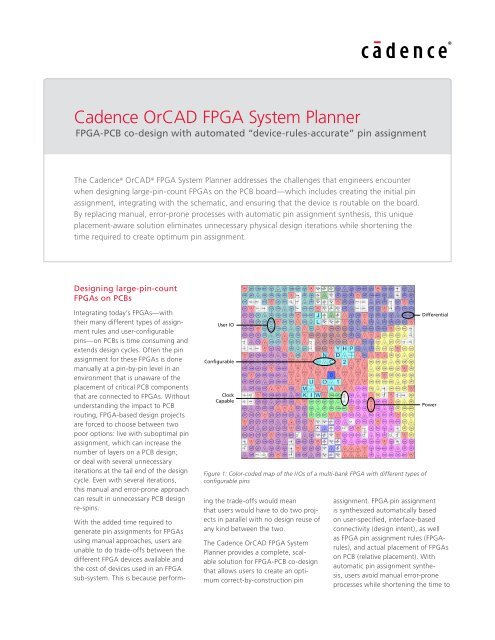
User IO<br />
Configurable<br />
Clock<br />
Capable<br />
Figure 1: Color-coded map of the I/Os of a multi-bank <strong>FPGA</strong> with different types of<br />
configurable pins<br />
ing the trade-offs would mean<br />
that users would have to do two projects<br />
in parallel with no design reuse of<br />
any kind between the two.<br />
The <strong>Cadence</strong> <strong>OrCAD</strong> <strong>FPGA</strong> <strong>System</strong><br />
<strong>Planner</strong> provides a complete, scalable<br />
solution for <strong>FPGA</strong>-PCB co-design<br />
that allows users to create an optimum<br />
correct-by-construction pin<br />
Differential<br />
Power<br />
assignment. <strong>FPGA</strong> pin assignment<br />
is synthesized automatically based<br />
on user-specified, interface-based<br />
connectivity (design intent), as well<br />
as <strong>FPGA</strong> pin assignment rules (<strong>FPGA</strong>rules),<br />
and actual placement of <strong>FPGA</strong>s<br />
on PCB (relative placement). With<br />
automatic pin assignment synthesis,<br />
users avoid manual error-prone<br />
processes while shortening the time to
create initial pin assignment that accounts<br />
for <strong>FPGA</strong> placement on the PCB (placement-aware<br />
pin assignment synthesis).<br />
This unique placement-aware pin assignment<br />
approach eliminates unnecessary<br />
physical design iterations that are inherent<br />
in manual approaches.<br />
The <strong>OrCAD</strong> <strong>FPGA</strong> <strong>System</strong> <strong>Planner</strong> is integrated<br />
with both <strong>OrCAD</strong> Capture and<br />
<strong>OrCAD</strong> PCB Editor. It reads and creates<br />
Capture schematics and symbols. In<br />
addition, a floorplan view uses existing<br />
footprint libraries from <strong>OrCAD</strong> PCB Editor.<br />
Should placement change during layout,<br />
pin optimization using <strong>FPGA</strong> <strong>System</strong><br />
<strong>Planner</strong> can be accessed directly from<br />
<strong>OrCAD</strong> PCB Editor.<br />
Benefits<br />
• Scalable, cost-effective <strong>FPGA</strong>-PCB<br />
co-design solution from <strong>OrCAD</strong> to<br />
Allegro ® GXL<br />
• Shortens time for optimum initial pin<br />
assignment, accelerating PCB design<br />
schedules<br />
• Accelerates integration of <strong>FPGA</strong>s<br />
with <strong>OrCAD</strong> PCB design creation<br />
environments<br />
• Eliminates unnecessary, frustrating<br />
design iterations during the PCB layout<br />
process<br />
• Eliminates unnecessary physical<br />
prototype iterations due to <strong>FPGA</strong> pin<br />
assignment errors<br />
• Reduces PCB layer count through<br />
placement aware pin assignment and<br />
optimization<br />
Features<br />
<strong>OrCAD</strong> <strong>FPGA</strong> <strong>System</strong> <strong>Planner</strong><br />
Technology<br />
An <strong>FPGA</strong> system is defined as a subset of<br />
the PCB design that includes one or more<br />
<strong>FPGA</strong> and non-<strong>FPGA</strong> components that are<br />
connected to <strong>FPGA</strong>s.<br />
Traditional approaches to pin assignment<br />
are typically manual and often based<br />
on a spreadsheet. Tools such as these<br />
require users to do pin assignment without<br />
taking into consideration the placement<br />
of other components and routability<br />
of the interfaces and signals. Above<br />
<strong>Cadence</strong> <strong>OrCAD</strong> <strong>FPGA</strong> <strong>System</strong> <strong>Planner</strong><br />
Figure 2: Placement/Floorplan view of the <strong>OrCAD</strong> <strong>FPGA</strong> <strong>System</strong> <strong>Planner</strong> provides users relative<br />
placement of critical components for optimum pin assignment synthesis<br />
all, there is no online rules-checking to<br />
ensure that the right pin types are being<br />
used for the signals that are assigned to<br />
the <strong>FPGA</strong> pins. As a result, users have<br />
to make several iterations between the<br />
spreadsheet-based tools and the tools<br />
from <strong>FPGA</strong> vendors. Often this adds an<br />
increased number of iterations between<br />
the PCB layout designer who cannot<br />
route the signals from <strong>FPGA</strong> pins on<br />
available layers and the <strong>FPGA</strong> designer<br />
who has to accept paper-based or verbal<br />
pin-assignment suggestions from the<br />
PCB layout designer. Once a change is<br />
made to the pin assignment by the <strong>FPGA</strong><br />
designer, the pin assignment change<br />
has to be made in the schematic design<br />
by the hardware designer. Such iterations<br />
add several days if not weeks to the<br />
design cycle and possibly a great deal of<br />
frustration for the team members. Since<br />
this is a manual process, mistakes that are<br />
not detected can also cause expensive<br />
physical prototype iterations.<br />
While it may help to automate the<br />
synchronization of changes made to the<br />
pin assignment by the <strong>FPGA</strong> designer,<br />
hardware designer, or PCB layout<br />
designer, it doesn’t reduce the root cause<br />
of these iterations. Pin assignment that<br />
is not guided by all three aspects—<strong>FPGA</strong><br />
resource availability, <strong>FPGA</strong> vendor pin<br />
assignment rules, and routability of <strong>FPGA</strong><br />
pins on a PCB—requires many iterations<br />
at the tail end of the design process,<br />
thereby extending the time it takes to<br />
integrate today’s complex, large-pincount<br />
<strong>FPGA</strong>s on a PCB.<br />
Specifying Design Intent<br />
The <strong>OrCAD</strong> <strong>FPGA</strong> <strong>System</strong> <strong>Planner</strong> comes<br />
with an <strong>FPGA</strong> device library to help with<br />
selection of devices to be placed. It uses<br />
<strong>OrCAD</strong> PCB Editor footprints for the<br />
floorplan view and allows users to quickly<br />
create relative placement of the <strong>FPGA</strong><br />
system components.<br />
The <strong>OrCAD</strong> <strong>FPGA</strong> <strong>System</strong> <strong>Planner</strong> allows<br />
users to specify connectivity between<br />
components within the <strong>FPGA</strong> sub-system<br />
at a higher level through interface definitions.<br />
Users can create interfaces such as<br />
DDR2, DDR3, and PCI Express, and use<br />
these to specify connectivity between an<br />
<strong>FPGA</strong> and a memory DIMM module or<br />
between two <strong>FPGA</strong>s. The <strong>OrCAD</strong> <strong>FPGA</strong><br />
<strong>System</strong> <strong>Planner</strong> understands differential<br />
signals, and power signals, as well as<br />
clock signals.<br />
<strong>FPGA</strong> Device Rules<br />
The <strong>OrCAD</strong> <strong>FPGA</strong> <strong>System</strong> <strong>Planner</strong> comes<br />
with a library of device-accurate <strong>FPGA</strong><br />
models that incorporate pin assignment<br />
rules and electrical rules specified by<br />
<strong>FPGA</strong> device vendors. These <strong>FPGA</strong> models<br />
are used by the synthesis engine to ensure<br />
that the vendor-defined electrical usage<br />
rules of the <strong>FPGA</strong>s are strictly adhered to.<br />
These rules dictate such things as clock<br />
www.cadence.com 2
<strong>FPGA</strong><br />
Vendor<br />
Tools<br />
and clock region selection, bank allocation,<br />
SSO budgeting, buffer driver utilization,<br />
I/O standard voltage reference<br />
levels, etc. During synthesis, the <strong>OrCAD</strong><br />
<strong>FPGA</strong> <strong>System</strong> <strong>Planner</strong> automatically<br />
checks hundreds of combinations of these<br />
rules to ensure that the <strong>FPGA</strong> pins are<br />
optimally and accurately utilized.<br />
Placement Aware Pin<br />
Assignment Synthesis<br />
<strong>OrCAD</strong><br />
<strong>FPGA</strong><br />
<strong>System</strong> <strong>Planner</strong><br />
The <strong>OrCAD</strong> <strong>FPGA</strong> <strong>System</strong> <strong>Planner</strong> provides<br />
users a way to create an <strong>FPGA</strong> system<br />
placement view using <strong>OrCAD</strong> PCB footprints.<br />
Users specify connectivity between<br />
components in the placement view and<br />
the <strong>FPGA</strong> at a high level using interfaces<br />
such as DDRx, PCI Express, SATA, Front<br />
Side Bus, etc. that connect <strong>FPGA</strong>s and<br />
other components in the design, shortening<br />
the time to specify design intent for<br />
the <strong>FPGA</strong> system.<br />
Once the connectivity of the <strong>FPGA</strong> to<br />
other components in the sub-system is<br />
defined, the <strong>OrCAD</strong> <strong>FPGA</strong> <strong>System</strong> <strong>Planner</strong><br />
then synthesizes the pin assignment<br />
based on the user’s design intent, available<br />
<strong>FPGA</strong> resources, component placement<br />
around the <strong>FPGA</strong>, and the <strong>FPGA</strong><br />
vendor’s pin assignment rules.<br />
The <strong>OrCAD</strong> <strong>FPGA</strong> <strong>System</strong> <strong>Planner</strong> has a<br />
built-in DRC engine that incorporates the<br />
rules provided by <strong>FPGA</strong> vendors for pin<br />
assignment, reference voltages, and terminations.<br />
This rules-based engine prevents<br />
PCB physical prototype iterations as the<br />
<strong>FPGA</strong>s are always correctly connected.<br />
<strong>OrCAD</strong><br />
Capture/CIS<br />
<strong>OrCAD</strong><br />
Part Library<br />
Symbols, Footprints<br />
<strong>OrCAD</strong><br />
PCB<br />
Designer<br />
Figure 3: The <strong>OrCAD</strong> <strong>FPGA</strong> <strong>System</strong> <strong>Planner</strong> uses symbols and footprints from existing libraries<br />
Pin assignment algorithms are optimized<br />
to assign interface signals to a group of<br />
pins, thereby minimizing net crossovers<br />
and improving routability on the PCB.<br />
Tight Integration with <strong>Cadence</strong><br />
Design Creation<br />
The <strong>OrCAD</strong> <strong>FPGA</strong> <strong>System</strong> <strong>Planner</strong> generates<br />
<strong>OrCAD</strong> Capture, schematics for the<br />
<strong>FPGA</strong> sub-system. It uses existing symbols<br />
Figure 4: <strong>OrCAD</strong> <strong>FPGA</strong> <strong>System</strong> <strong>Planner</strong> optimization<br />
<strong>Cadence</strong> <strong>OrCAD</strong> <strong>FPGA</strong> <strong>System</strong> <strong>Planner</strong><br />
for <strong>FPGA</strong> in <strong>OrCAD</strong> Capture symbol<br />
libraries. If the user desires, the <strong>FPGA</strong><br />
<strong>System</strong> <strong>Planner</strong> products can create split<br />
symbols for <strong>FPGA</strong> based on the connectivity<br />
or one split symbol per bank.<br />
Integration with <strong>FPGA</strong><br />
Vendor Tools<br />
In addition to integration with <strong>OrCAD</strong><br />
PCB design tools, the <strong>OrCAD</strong> <strong>FPGA</strong><br />
<strong>System</strong> <strong>Planner</strong> communicates seamlessly<br />
with <strong>FPGA</strong> design tools. It generates<br />
and reads supported <strong>FPGA</strong> vendors’ pin<br />
assignment constraint files. This capability<br />
enables the <strong>FPGA</strong> designer to evaluate<br />
pin assignments against the functional<br />
needs of the <strong>FPGA</strong>. Any changes made<br />
by the <strong>FPGA</strong> designer to account for<br />
these requirements can be imported into<br />
to the <strong>OrCAD</strong> <strong>FPGA</strong> <strong>System</strong> <strong>Planner</strong> so<br />
that the complete set of pin assignments<br />
remain in sync.<br />
www.cadence.com 3
Pre-Route Pin Assignment<br />
Optimization<br />
The initial pin assignment—that accounts<br />
for placement and routability of the <strong>FPGA</strong><br />
on a PCB—goes a long way toward<br />
reducing costly design iterations between<br />
<strong>FPGA</strong> designer, PCB layout designer, and<br />
hardware designer. Once the PCB layout<br />
designer starts to plan the routing of interfaces<br />
and signals on <strong>FPGA</strong>, it is possible<br />
to further refine the <strong>FPGA</strong> pin assignment<br />
based on route intent, layer constraints,<br />
and fanout chosen for the <strong>FPGA</strong>. The<br />
<strong>OrCAD</strong> <strong>FPGA</strong> <strong>System</strong> <strong>Planner</strong> offers users a<br />
way to optimize <strong>FPGA</strong> pin assignment after<br />
placement and during routing of the interfaces<br />
and signals on an <strong>FPGA</strong>.<br />
Concurrent device<br />
optimization<br />
Placement-aware<br />
synthesis<br />
Reuse symbols and<br />
footprints<br />
Symbols and<br />
schematic generation<br />
Post-placement<br />
optimization<br />
Schematic power<br />
connections<br />
<strong>OrCAD</strong> <strong>FPGA</strong> <strong>System</strong><br />
<strong>Planner</strong><br />
1 <strong>FPGA</strong> or Multiple<br />
<strong>FPGA</strong>s totaling 1,000<br />
max pins<br />
Scalability<br />
The <strong>OrCAD</strong> and Allegro <strong>FPGA</strong> <strong>System</strong><br />
<strong>Planner</strong> technology is available in the<br />
following product offerings:<br />
• Allegro <strong>FPGA</strong> <strong>System</strong> <strong>Planner</strong> GXL—<br />
for synthesizing and optimizing pin<br />
assignment of more than four <strong>FPGA</strong>s at<br />
a time. Suitable for companies that use<br />
<strong>FPGA</strong>s to prototype ASICs<br />
• Allegro <strong>FPGA</strong> <strong>System</strong> <strong>Planner</strong> XL—for<br />
concurrent pin assignment, synthesis,<br />
and post-placement optimization of up<br />
to four <strong>FPGA</strong>s at a time<br />
• Allegro <strong>FPGA</strong> <strong>System</strong> <strong>Planner</strong> L—for pin<br />
assignment synthesis and post-placement<br />
optimization of a single <strong>FPGA</strong><br />
• <strong>OrCAD</strong> <strong>FPGA</strong> <strong>System</strong> <strong>Planner</strong>—for<br />
optimum initial pin assignment<br />
synthesis of a single <strong>FPGA</strong>.<br />
Allegro 2 <strong>FPGA</strong><br />
<strong>System</strong> <strong>Planner</strong><br />
Option<br />
2 <strong>FPGA</strong>s or Multiple<br />
<strong>FPGA</strong>s totaling 2,000<br />
max pins<br />
<strong>Cadence</strong> <strong>OrCAD</strong> <strong>FPGA</strong> <strong>System</strong> <strong>Planner</strong><br />
Sales, Technical Support, and<br />
Training<br />
The <strong>OrCAD</strong> product line is owned by<br />
<strong>Cadence</strong> Design <strong>System</strong>s, Inc., and<br />
supported by a worldwide network of<br />
<strong>Cadence</strong> Channel Partners (VARs). For<br />
sales, technical support, or training,<br />
contact your local <strong>Cadence</strong> Channel<br />
Partner. For a complete list of authorized<br />
<strong>Cadence</strong> Channel Partners, visit<br />
www.cadence.com/Alliances/channel_<br />
partner.<br />
Allegro 4 <strong>FPGA</strong><br />
<strong>System</strong> <strong>Planner</strong><br />
Option<br />
4 <strong>FPGA</strong>s or Multiple<br />
<strong>FPGA</strong>s totaling 4,000<br />
max pins<br />
Allegro ASIC<br />
Prototyping Option<br />
Unlimited <strong>FPGA</strong>s<br />
Yes Yes Yes Yes<br />
Yes Yes Yes Yes<br />
<strong>OrCAD</strong> Capture<br />
Allegro Design Entry CIS<br />
/ Allegro Design Entry<br />
HDL<br />
Allegro Design Entry CIS<br />
/ Allegro Design Entry<br />
HDL<br />
Allegro Design Entry CIS<br />
/ Allegro Design Entry<br />
HDL<br />
No Yes Yes Yes<br />
No Yes Yes Yes<br />
<strong>Cadence</strong> is transforming the global electronics industry through a vision called EDA360.<br />
With an application-driven approach to design, our software, hardware, IP, and services help<br />
customers realize silicon, SoCs, and complete systems efficiently and profitably. www.cadence.com<br />
© 2011 <strong>Cadence</strong> Design <strong>System</strong>s, Inc. All rights reserved. <strong>Cadence</strong>, the <strong>Cadence</strong> logo, Allegro, and <strong>OrCAD</strong> are registered trademarks of <strong>Cadence</strong><br />
Design <strong>System</strong>s, Inc., All rights reserved. 22239 06/11 MK/DM/PDF