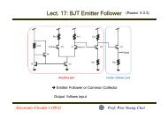
Lect. 22: MOSFET Small-Signal Model (2)
Lect. 22: MOSFET Small-Signal Model (2)
Lect. 22: MOSFET Small-Signal Model (2)
- No tags were found...

Create successful ePaper yourself
Turn your PDF publications into a flip-book with our unique Google optimized e-Paper software.
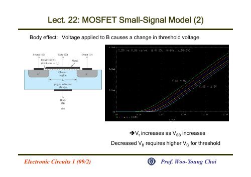
<strong>Lect</strong>. <strong>22</strong>: <strong>MOSFET</strong> <strong>Small</strong>-<strong>Signal</strong> <strong>Model</strong> (2)Body effect: Voltage applied to B causes a change in threshold voltageV t increases as V SB increasesDecreased V B requires higher V G for thresholdElectronic Circuits 1 (09/2)Prof. Woo-Young Choi
<strong>Lect</strong>. <strong>22</strong>: <strong>MOSFET</strong> <strong>Small</strong>-<strong>Signal</strong> <strong>Model</strong> (2)Body effect:V = V + γ[ 2φ + V − 2 φ ]t tO f SB fV = V when V = 0φt tO SBfand γ process-dependent parametersIf S and B can be tied, no body effect.In ICs, B is connected to- the most negative supply voltage (NMOS)- the most positive supply voltage (PMOS)Electronic Circuits 1 (09/2)Prof. Woo-Young Choi
<strong>Lect</strong>. <strong>22</strong>: <strong>MOSFET</strong> <strong>Small</strong>-<strong>Signal</strong> <strong>Model</strong> (2)<strong>Small</strong>-signal model including Body effectPractically, Body EffectIs not easy to model analytically.ygmb∂i≡ ∂DυBS υ =υ =GSDSconstantconstant Simulationgmb≡χ gm( χ :0.1−0.3)Electronic Circuits 1 (09/2)Prof. Woo-Young Choi
<strong>Lect</strong>. <strong>22</strong>: <strong>MOSFET</strong> <strong>Small</strong>-<strong>Signal</strong> <strong>Model</strong> (2)High-Frequency <strong>Model</strong> for <strong>MOSFET</strong>Unit-Gain Frequency (f t ):Frequency at which magnitude of the short-circuit current gain of CS configuration becomes 1Or Mag(I o (ω)/I i (ω)) = 1Electronic Circuits 1 (09/2)Prof. Woo-Young Choi
<strong>Lect</strong>. <strong>22</strong>: <strong>MOSFET</strong> <strong>Small</strong>-<strong>Signal</strong> <strong>Model</strong> (2)How fast can a <strong>MOSFET</strong> transistor operate? f tVI g V g V j C V g V g C1jωCgs0=m gs− =m gs− ωgd gs=m gs( Qm>> ωgdgd⎛ 1 1 ⎞ 1Vgs = Ii ⋅ || = Ii⋅⎜ jωCgd jωC ⎟⎝gS ⎠ jω( Cgd + Cgs)I0gm∴ =I jω( C + C )i gd gsI0gmFor = 1, ω =I C + Ci gd gsgmOr fT=(Unit-gain Frequency)2 π ( Cgd+Cgs)How to make <strong>MOSFET</strong> faster?Which is faster NMOS or PMOS?Current state-of-the-art the art NMOS has f T approaching 100 GHz.Electronic Circuits 1 (09/2)Prof. Woo-Young Choi
<strong>Lect</strong>. <strong>22</strong>: <strong>MOSFET</strong> <strong>Small</strong>-<strong>Signal</strong> <strong>Model</strong> (2)- Modern transistors are verycomplicated in their structure.- Many parameters are needed tomodel their characteristicsaccurately in SPICE- SPICE parameters for0.25μm NMOS are shown- For detailed explanations,See <strong>MOSFET</strong> Users’ Manual atwww-device.eecs.berkeley.edu/eecs edu/~bsim3/get.htmlMODEL orbit2L2N NMOS ( LEVEL = 7+TNOM = 27 TOX = 5.6E-9+XJ = 1E-7 NCH = 2.3549E17 VTH0 = 0.3654765+K1 = 0.473<strong>22</strong>14 K2 = 7.994532E-4 K3 = 1E-3+K3B = 3.0713494 W0 = 1E-7 NLX = 1.617898E-77+DVT0W = 0 DVT1W = 0 DVT2W = 0+DVT0 = 0.455178 DVT1 = 0.6258687 DVT2 = -0.5+U0 = 280.4589023 UA = -1.607126E-9 UB = 2.806549E-18+UC = 3.290051E-11 VSAT = 1.07496E5 A0 = 1.8770435+AGS = 0.3310181 B0 = -3.173524E-8 B1 = -1E-7+KETA = -8.69841E-3 A1 = 8.317145E-5 A2 = 0.6592347+RDSW = 200 PRWG = 0.4477477 PRWB = 0.0208175+WR = 1 WINT = 0 LINT = 1.392558E-10+DWG = -2.28419E-8+DWB = -6.95781E-10 VOFF = -0.0910963 NFACTOR = 1.202941+CIT = 0 CDSC = 2.4E-4 4 CDSCD = 0+CDSCB = 0 ETA0 = 5.0732E-3 ETAB = 6.262008E-5+DSUB = 0.0310034 PCLM = 1.5101091 PDIBLC1 = 0.897659+PDIBLC2 = 2.924029E-3 PDIBLCB = 0.0651312 DROUT = 1+PSCBE1 = 7.017738E8 PSCBE2 = 2.271109E-4 PVAG = 8.531511E-3+DELTA = 0.01 RSH = 4.6 MOBMOD = 1+PRT = 0 UTE = -1.5 15 KT1 = -0.11 011+KT1L = 0 KT2 = 0.0<strong>22</strong> UA1 = 4.31E-9+UB1 = -7.61E-18 UC1 = -5.6E-11 AT = 3.3E4+WL = 0 WLN = 1 WW = 0+WWN = 1 WWL = 0 LL = 0+LLN = 1 LW = 0 LWN = 1+LWL = 0 CAPMOD = 2 XPART = 0.5+CGDO = 4.59E-10 CGSO = 4.59E-10 CGBO = 5E-10+CJ = 1.78338E-3 PB = 0.99 MJ = 0.4661295+CJSW = 4.154041E-10 PBSW = 0.9563049 MJSW = 0.3162462+CF = 0 PVTH0 = -9.648921E-3 PRDSW = -10+PK2 = 3.534961E-3 WKETA = 0.01209810120981 LKETA = -3.31688E-331688E-3 )Electronic Circuits 1 (09/2)Prof. Woo-Young Choi
<strong>Lect</strong>. <strong>22</strong>: <strong>MOSFET</strong> <strong>Small</strong>-<strong>Signal</strong> <strong>Model</strong> (2)How to do PSPICE simulation? Instructions will be given during next tutorial (11/9)Bring your own notebook computer if you canElectronic Circuits 1 (09/2)Prof. Woo-Young Choi