Chip Scale Review - October 2008
Chip Scale Review - October 2008
Chip Scale Review - October 2008
- No tags were found...

You also want an ePaper? Increase the reach of your titles
YUMPU automatically turns print PDFs into web optimized ePapers that Google loves.
<strong>October</strong> <strong>2008</strong>• High-Speed Bond Testing• Wafer Probing Advances
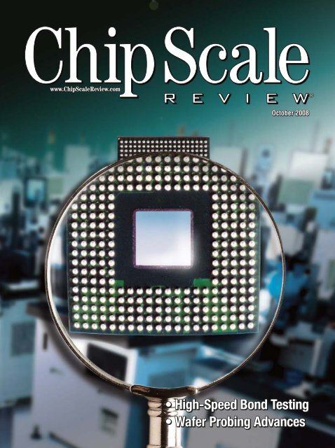
CONTENTS<strong>October</strong> <strong>2008</strong>Volume 12, Number 7The international magazine for device and wafer-level test, assemblyand packaging that addresses high-density interconnection of microelectronicsICs, MEMS, RF/wireless, optoelectronic and other wafer-fabricated devicesfor the 21st Century.FEATURE ARTICLESInternational Directory of Wafer Probers and Probe Cards<strong>Chip</strong> <strong>Scale</strong> <strong>Review</strong> Staff26THE COVERThis is <strong>Chip</strong> <strong>Scale</strong> <strong>Review</strong>’s inspection issue.This issue’s cover graphically representsprobing and test.That conveniently ties in with the“Probe Mark Analysis—A Critical Windowon Actual Probe Card Performance” articleby Darren James, Product Manager,Rudolph Technologies Inc. Probe markanalysis provides a critical window on actualprobe performance, allowing engineersto optimize probing processes and realizesubstantial economic returns.The insightful “High-Speed Wire BondTesting: Understanding the Technology”article by Bob Sykes, Dage PrecisionIndustries, Ltd. follows with details on howto be certain that your wire bonding integrityis as intended. A comprehensive knowledgeof bond strength, force displacement andenergy measurement of solder ball bonds iscritical for the detection of brittle fracturefailures within semiconductor packages.PCA OTWafer Scrub EPCA & ScrubCenter PositioWafer Scrub StPCA NOTProbe Mark Analysis—A Critical Window 29on Actual Probe Card PerformanceDarren James, Rudolph Technologies Inc.Probe mark analysis provides a critical window on actual probeperformance, allowing engineers to optimize probing processes andrealize substantial economic returns. Systematic discrepancies betweenprobe card test data and actual on-wafer performance can be correctedto improve visibility of the probing process.International Directory of Failure Analysis/DefectInspection System Suppliers<strong>Chip</strong> <strong>Scale</strong> <strong>Review</strong> Staff36High-Speed Bondtesting:42Understanding the TechnologyBob Sykes, Dage Precision Industries Ltd.Bond failures indicate loads on the bond and excessive strain rates.However, weak or poor quality bonds can fail even at low forces. Thekey is determining at what force and energy they fail. A comprehensiveknowledge of bond strength, force displacement and energy measurementof solder ball bonds is critical for the detection of brittle fracture failureswithin semiconductor packages.CONTINUED >>(Illustration for <strong>Chip</strong> <strong>Scale</strong> <strong>Review</strong> byDesign 2 Market) [design2marketinc.com]<strong>Chip</strong> <strong>Scale</strong> <strong>Review</strong>, at 7291 Coronado Dr., Suite 8, San Jose, CA 95129(ISSN 1526-1344), is published eight times a year, with issues inJanuary-February, March, April, May-June, July, August-September,<strong>October</strong> and November-December.Periodical postage paid at San Jose, Calif., and additional offices.POSTMASTER: Send address changes to <strong>Chip</strong> <strong>Scale</strong> <strong>Review</strong> magazine,7291 Coronado Dr., Suite 8, San Jose, CA 95129.<strong>Chip</strong> <strong>Scale</strong> <strong>Review</strong> ■ <strong>October</strong> <strong>2008</strong> ■ [<strong>Chip</strong><strong>Scale</strong><strong>Review</strong>.com] 1
COMMENTARYNew DistinguishedEditorial Advisors Join<strong>Chip</strong> <strong>Scale</strong> <strong>Review</strong>By Terrence E. Thompson, Editor in Chief [tethompson@aol.com]and Kim Newman, Publisher and Sales Manager [csradv@aol.com]<strong>Chip</strong> <strong>Scale</strong> <strong>Review</strong> is honored to announce the addition of two new distinguishedEditorial Advisory Board members: Lee Smith, Vice President of BusinessDevelopment at Amkor Technology Inc. [amkor.com] and Dr. Andy Mackie, ProductManager, Semiconductor Packaging Materials at Indium Corporation [indium.com].Both have extraordinary assembly and packaging insights that will help shape CSR’s editorialfocus as the magazine and the industries we serve move forward to face new challengesand opportunities.Their insights will help CSR better target emerging opportunity areas for those nowprimarily involved in chip (the many devices including ICs) and wafer-level assembly/packaging(WLP) operations. We will, as always, thoroughly address today’s mainstream assemblyand packaging processes and materials to address immediate challenges.Of course, virtually every technology product or service we use today is microelectronicscentric.Ongoing innovations in device and wafer-level test, assembly and packaging areessential to keep up with the ITRS roadmap growth goals anticipated for microelectronicsinterconnects and packaging innovations as well as related emerging technologies includingMEMS/MOEMS and nanotech where IC manufacturing expertise can bring aboutdesired change and progress more quickly.Our own bias is that materials science and engineering are crucial areas that will leadthe way in making future technology advancements both possible and affordable. Theinevitable challenges that high-tech companies will face as IC thin films become ever thinnerand feature sizes continue to shrink are both obvious and subtle.Basic materials behavior changes as bulk sizes decrease and quantum mechanics effectscome into play. In most cases, assembly process temperatures become much more critical.Since many lead-free solders require higher reflow temperatures, more users may be evaluatingsolders more closely than ever.Process equipment is indeed crucial for packaging success. However, most advances inequipment are evolutionary although steady streams of new machines make the processingmore efficient and cost effective.Andy’s insights on advanced materials will help guide our editorial direction. Lee’s insightson assembly and packaging processes as well as the requisite production hardware areinvaluable. Both are well-known and respected industry experts with perspectives thatwill provide guidance for CSR’s ongoing editorial direction. Both will author CSR articlesin 2009 so watch for them! i2<strong>Chip</strong> <strong>Scale</strong> <strong>Review</strong> ■ <strong>October</strong> <strong>2008</strong> ■ [<strong>Chip</strong><strong>Scale</strong><strong>Review</strong>.com]STAFFVOLUME 12, NUMBER 7The international magazine for device and waferleveltest, assembly and packaging that addresseshigh-density interconnection of microelectronics ICs,MEMS, RF/wireless, optoelectronic and other waferfabricateddevices for the 21st century.Kim Newman Publisher/Sales Manager7291 Coronado Dr., Ste. 8, San Jose, CA 95129b 1.408.996.7016 > 1.408.996.7871csradv@aol.comTerrence Thompson Editor in Chief2303 Randall Rd. #140, Carpentersville, IL 60110b 1.847.515.1255tethompson@aol.comMartin Kraft Technical Editormartykraft@aol.comSteve Berry Contributing Editorb 1.408.369.7000 > 1.408.369.8021saberry@electronictrendpubs.comDr. Tom Di Stefano Contributing Editorb 1.408.399.4501 > 1.408.395.0448tom@centipedesystems.comPaul M. Sakamoto Contributing Editor–Testpaul.sakamoto@comcast.comSandra Winkler Contributing Editorb 1.408.369.7000 > 1.408.369.8021slwinkler@electronictrendpubs.comThe Official Publication of the WLCSP ForumSUBSCRIPTION INQUIRIESJudy Levin <strong>Chip</strong> <strong>Scale</strong> <strong>Review</strong>7291 Coronado Dr., Ste. 8, San Jose, CA 95129b 1.408.996.7016 > 1.408.996.7871csrsubs@chipscalereview.comADVERTISING PRODUCTIONINQUIRIES AND REPRINTSKim Newman7291 Coronado Dr., Ste. 8, San Jose, CA 95129b 1.408.996.7016 > 1.408.996.7871csradv@aol.comADVISORSDr. Tom Di Stefano Centipede SystemsLee Smith Amkor Technology Inc.Dr. Andy C. Mackie Indium CorporationCharles R. Harper Technology Seminars Inc.Dr. Guna Selvaduray San Jose State UniversityDr. Thorsten Teutsch Pac Tech USADr. David Tuckerman Tessera TechnologiesProfessor C.P. Wong Georgia TechCopyright © <strong>2008</strong> by Gene Selven & Associates Inc.<strong>Chip</strong> <strong>Scale</strong> <strong>Review</strong> (ISSN 1526-1344) is a registered trademarkof Gene Selven & Associates Inc. Publishing headquarters arelocated at 7291 Coronado Drive, Suite 8, San Jose, CA 95129.All rights reserved.<strong>Chip</strong> <strong>Scale</strong> <strong>Review</strong> is published eight times a year.Subscriptions in the U.S. are available without charge toqualified individuals in the electronics industry. Subscriptionsoutside the U.S. (eight issues) by airmail are $60 per year toCanada or $60 to other countries. In the U.S., subscriptionsby first class mail are $40 per year.
CONTENTSFEATURED DEPARTMENTWLCSP Forum: Trends in Wafer Level 22<strong>Chip</strong> <strong>Scale</strong> PackagingL. Nguyen, National Semiconductor Corp.;T. Tessier, Flip <strong>Chip</strong> International; H. Theuss, Infineon;R. Haas and K. Baker, California Micro Devices“The best package is no package” is a simple butmeaningful description of the basic idea to fabricatea complete electrical component on wafer level prior to dicing.In a Wafer Level <strong>Chip</strong> <strong>Scale</strong> Package (WLCSP), all packaging andinterconnection are done using wafer processes. Thus, cost-intensivesequential processes like die and wirebonding are replaced. WLCSPs areshipped after electrical testing and mounted directly onto a PCB usingstandard pick and place technology, preferably without underfill.DEPARTMENTSCommentary Terrence Thompson and Kim NewmanNew Distinguished Editorial Advisors Join <strong>Chip</strong> <strong>Scale</strong> <strong>Review</strong>Assembly Lines Terrence ThompsonMartin Kraft Joins the <strong>Chip</strong> <strong>Scale</strong> <strong>Review</strong> Editorial Staff; 5th Annual IWLPCInside Patents A. Jason Mirabito and Carol PetersWafer Probe Interconnect System-Resolving Wafer Warp IssuesIndustry NewsCalendar2681618If you’re involved in IC or MEMS packaging, thisyear’s IWLPC is the conference you should not miss!SA N JOSE, CALIFO R NIA<strong>October</strong> 13-16, <strong>2008</strong>San Jose, CaliforniaCo-presented byElectronic Trends Steve Berry and Sandra WinklerIC Applications—Solid Volume Increases, More Growth to ComeWhat’s New!Product Showcase (Advertisement)213446O C T O B E R 1 3-1 6, 2 0 0 8Visit IWLPC.COM for detailsAd Index/More News/Sales Offices48<strong>Chip</strong> <strong>Scale</strong> <strong>Review</strong> ■ <strong>October</strong> <strong>2008</strong> ■ [<strong>Chip</strong><strong>Scale</strong><strong>Review</strong>.com] 3
SSEC Single WaferSingle Wafer ProcessingSSEC Systems are configurable in strip, etch and clean process stations withup to 12 stations in a system. In a Class 1 mini-environment, dual SCARArobotics can operate in any sequence to any station according to recipeselection. SSEC’s applications laboratory will assist you in configuring a toolaround your exact process and manufacturing requirements.Come visit SSEC and learn what is new in single wafer processing.wet processingClean99% Particle Removal Efficiency atthe 88 nm, 65 nm, and 45 nm NodesDual SCARA robotics can addressall stations in any sequence.Solvent StripImmersion and SingleWafer ProcessingSSEC 33011 Processing StationSSEC 3303/43-4 Processing StationsEtchUniform, Selective Etching onMultiple Process LevelsSSEC 33077 Processing StationsSSEC ComplianceSEMI S2-0706E SafetySEMI S8-0705E ErgonomicsFM 4910 MaterialsSECS GEM CCS 200 & 300CE MarkedETL ListedSSEC 331010 Processing StationsCoat/DevelopPhotolithography Clusterswww.ssecusa.comPhone: 215-328-0700
US # 6,539,952High Velocity Scrub Single Wafer Megasonic Scrub Rotary PVA Brush ScrubDouble-sided PVA BrushFor single-or double-sided particle clean, SSEC systems can be configured exactly to your cleaning requirements. Using dilute chemistries,such as SC-1 1:1:300, SSEC cleaning processors have 99% particle removal efficiency at the 88 nm, 65nm, and 45 nm nodes.High Pressure Flow ControlPressureSolvent Immersion High Pressure Spray High Pressure Needle DispenseTimeUsing only milliliters of solvent per wafer, SSEC solvent processors combine batch immersion and single wafer spray technology inone SEMI ® safety compliant, dry-in /dry-out system. High pressure sprays are entirely under closed-loop control for flow, temperature,and dispense arm motions.Ti EtchBackside/Bevel CleaningStream Flow EtchSpray EtchAl EtchCu EtchSingle Wafer Wet Etch with PC Program Control over Flow Rate, Temperature and Chemical Blending by recipe with per wafer selectivity. SSEC’spatent pending Chemical Collection System is over 90% effective for both single side and double sided processing. Each Wafer is processed underthe careful watch of a color CCD camera for adaptive process control with SSEC’s WaferChek System.Spin CoatingHot Plate Bake ProcessingMulti Size Hot PlateSpray DevelopCoat and Develop processors are configured to your exact production requirements, whether for double sided MEMs Coating or Thick ResistProcessing. With SSEC’s Vision Driven Wafer Alignment, Coat/Develop processors can change wafer sizes with only a PC recipe change- nohardware tooling changes. All Systems are fully robotic enabling recipe driven sequencing operation.3300
ASSEMBLY LINESMartin Kraft Joins the <strong>Chip</strong> <strong>Scale</strong> <strong>Review</strong> Editorial StaffBy Terrence Thompson, Editor in Chief [tethompson@aol.com]We enthusiastically welcomemy friend and colleaguefrom earlier publishingdays Martin (Marty) Kraft. He hasjoined the <strong>Chip</strong> <strong>Scale</strong> <strong>Review</strong> editorialstaff as Technical Editor. Marty has 25years of technical writing and editingexperience. Previously, he was theTechnical Editor for Circuits Assemblymagazine. Currently, he is the managingeditor for an international mechanicalengineering association. He has a MS intechnical communication and a BA injournalism.He’s already hard at work behind thescenes! He will make CSR a better magazinegoing forward.5th Annual IWLPC, Biggerand Better Than Ever!The 5th InternationalConference on Wafer-Level Packaging(IWLPC) with its 3DStacking focus is on track with its largerthan ever technical program, timely paneldiscussions and companion exhibitsthat address the products and servicesneeded by those in microelectronics,nanotech and emerging technologiesincluding photovoltaic production.SA N JOSE, CALIFO R NIAO C T O B E R 1 3-1 6, 2 0 0 8Batch or Discrete ManufacturingThis conference is all about how toselect and implement the “best” IC andwafer-level packaging (WLP) optionsfor a given application. For industryContinued on page 11 >>6<strong>Chip</strong> <strong>Scale</strong> <strong>Review</strong> ■ <strong>October</strong> <strong>2008</strong> ■ [<strong>Chip</strong><strong>Scale</strong><strong>Review</strong>.com]
INSIDE PATENTSWafer Probe Interconnect System—Resolving Wafer Warp IssuesBy A. Jason Mirabito [jmirabito@mintz.com] andCarol Peters [cpeters@mintz.com], Contributing Legal Editors,Mintz Levin Cohn Ferris Glovsky and Popeo P.C., Boston [mintz.com]Our column discusses theimprovements that U.S.Patent No. 7,382,143, issuedon June 3, <strong>2008</strong> and assigned on its faceto Centipede Systems, offers to resolveproblems related to wafer warp. In thepast, integrated circuit chips (“ICs”)were tested once the chips had beendiced and cut away from the wafer.Today, with WLP, it is becoming morecommon to test individual ICs whilethey remain on the wafer.Testing chips on the wafer allows theoperator to determine which wafersmeet specific electrical and functionaltests and to discard defective ICs beforethey are diced and mounted into semiconductorpackages. The problem thatoccurs with such testing is that, as semiconductorwafers are more and moredense, the geometries of ICs shrink andit becomes consequently more difficultto probe each of the desired pads on anindividual IC.Making Better Contact Is CrucialThe ‘143 patent describes a specificproblem with prior art probes in thatprobe heads under a load do not makeuniform contacts with the wafer due towarping of the wafer probe head.Consequently, incorrect or inaccuratetest results occur due to the incorrect orinadequate contacts, and this can causethe rejection of ICs that are good.According to the ‘143 patent, animprovement is offered by mounting a8<strong>Chip</strong> <strong>Scale</strong> <strong>Review</strong> ■ <strong>October</strong> <strong>2008</strong> ■ [<strong>Chip</strong><strong>Scale</strong><strong>Review</strong>.com]
number of posts on a rigid supportblock that inhibits warping of a substrateunder load. As illustrated in the figure, awafer probe interconnection apparatusis disclosed that includes pliant probetips a mounted on a number of dielectricsubstrates b. The substrates,according to the patent, could be fabricatedin different sizes in order toaccommodate a particular wafer beingtested. The wafer probe interconnectapparatus includes a plurality of dielectricsubstrates arrayed in a two-dimensionalpattern that may cover the surfaceof an entire wafer.The substrates may be fabricatedfrom alumina sheet material or otherdielectric materials, such as aluminumnitrate. Each substrate b is supportedby spring posts c. Each spring postcompresses, or is allowed to compress,to permiteach of thesubstrates bto align parallelto theplane of thewafer beingprobed. Eachof the springposts c holdeach of thesubstrates b above a support block d.The support block is, according to thepatent, selected for material propertiesincluding rigidity. The spring posts alsoare designed to be sufficiently pliantto allow for thermal expansion of thedielectric substrate b without thedielectric substrate being warped. Inaddition, flex cables e electrically coupleprobes a at contact terminals f.Improvements are obtained by mounting a number of posts on a rigid support blockthat inhibits the warping of a substrate under load.Finally, flat springs g are attached to amounting ring h and maintain tensionbetween support block d and levelingplate i.The ‘143 patent thus discloses a wafertesting apparatus that allows testing of anumber of uncut ICs on a semiconductorwafer in such a way that the probe tipsuniformly contact the contact surfaceson the undiced ICs. iFOR MICROWAVE DEVICE SOLDERING LOOK TOSikama InternationalThe World Leader in High Density Package Reflow OvensSikama International, Inc. • www.sikama.com<strong>Chip</strong> <strong>Scale</strong> <strong>Review</strong> ■ <strong>October</strong> <strong>2008</strong> ■ [<strong>Chip</strong><strong>Scale</strong><strong>Review</strong>.com] 9
MicrobondDocfish –same behaviora billion timesMaterials for WaferBumping ApplicationsPlease visit us atIMAPS ProvidenceBooth 52201883 www.aim.deUmicore AG & Co. KGMicrobond - EPMHanau · Singaporewww.microbond.euUltrafinepitchSolder PastesWatersoluble andNo Clean Flux SeriesSoft Solder Spheresfrom Duksan Hi-MetalA perfect fit !
ASSEMBLY LINESContinued from page 6 >>veterans, it’s obvious that any singlegiven packaging approach does not workfor everything. There’s a reason why wehave competing processes—they all workwell for some applications but not for all.The conference explores many processalternatives of interest to attendees.WLP itself has many subsets and thevariants are increasing. The WLP appealis obvious—it is batch (parallel) manufacturingprocess with enormous potentialeconomies of scale. WLP can redistributepads (RDL), bump, encapsulate,dice, etc., to produce a packaged deviceready for mounting on a PWB—or in a2D/3D SiP or in a PoP stack.High-Volume CustomizationSystem in Package (SiP) is a collectionof electrically interconnected andmechanically secured “chips” in 2Dand/or 3D arrangements on/in somesort of HDI (high-density interconnect)substrate. SiP can be quickly implementedfor fast-changing OEM products withmarket-driven quarterly, or even morefrequent, updates.System on <strong>Chip</strong> (SoC) is an elegantcollection of interconnected chipsformed on a wafer with an expensivemicroprocessor grade silicon wafer base.Potentially, SoC is an alternative to SiP.However, SoC design and fabricationusually are too slow for fast-changingOEM products with quarterly updates.However, SoC provides core functionalityfor some products including mobilephones and other high-volume productscan use SoCs in SiPs. If quick turnaroundsand the lowest possible costs are essential,SiP is probably a far better choice.Stack WLP-produced and/or standardpackages and you get PoP (Package-on-Package). With WLP, stacked wafers areoften thinned to minimize final packagethickness, essential for many low-profileform factor products. TSV (through siliconvia) vertical interconnects withinthe wafer and for wafer-to-wafer or dieto-diestacks are made with either “viafirst” and “via last” philosophies. Whichis best? We’re waiting to see.As the IWLPC speakers and instructorswill suggest, the “best” option is whatworks for you within your budget andmeets performance and reliability criteria!Affordable and ReliableWe need economies of scale, assembly/packaging schemes with a high probabilityof working right the first time, flexibilityContinued on page 13 >><strong>Chip</strong> <strong>Scale</strong> <strong>Review</strong> ■ <strong>October</strong> <strong>2008</strong> ■ [<strong>Chip</strong><strong>Scale</strong><strong>Review</strong>.com] 11
Automatic In-line Wire Bond InspectionHigh accuracy inspectionof wire bond connectionsViscom’s in-line automatic opticalinspection (AOI) system S6053BOguarantees reliable defect detectionon typical bond connections. Withits modular camera technologyand standard resolutions of 8.3μm or5.6μm, the system inspects over1,000 aluminum or gold wireconnections per minute as well asSMD components, solder joints anddie damages. For wire diameters downto 17μm, the new VHR cameramodule with resolutions < 3μm isnow available. Viscom’s field-provenS6053BO AOI system is able toreliably inspect features such asball or wedge position andcompleteness, loop-height, spacing,shape and geometry and ensureshighest quality in zero defectenvironments.See us atIMAPS <strong>2008</strong>,November 4-6,Rhode Island
ASSEMBLY LINESContinued from page 11 >>to handle constant product updates/innovation and the infrastructureto make it happen. Today’s mainstream technologyproducts are “microelectronics centric,” i.e., they don’t workwithout electronics for I/O control and electrical power.What, exactly, are you packaging, and how is what youmust ask yourself? So why not keep packaging one chip at atime? Or batch package chips? Or package multiple chips? Orbetter yet—any and all as needed.Don’t miss the conference since it will help answer the manycrucial questions that those making the most sophisticatedpackages in the world! [iwlpc.com] or [smta.org]DuPont Electronic TechnologiesExpands WLP PortfolioResearch Triangle Park, N.C.—DuPont Electronic Technologieshas expanded its focus on materials for wafer level packagingand emerging 3D and through silicon via (TSV) semiconductorpackaging including copper pillar and solder bump applications.DuPont is developing new products, new partnerships and isexpanding its technical capability to support the growingglobal demand for advanced materials in the semiconductorindustry.“Our goal is to reduce customer cycle time for new processdevelopment and implementation by offering innovative, testedand compatible material sets based on technology from acrossDuPont as well as in cooperation with our strategic industrypartners,” said Mats J. Ehlin, global business manage, DuPontWafer Level Packaging. “The semiconductor packaging marketis recognized as a strategic area of growth within DuPont, andwe’re excited about expanding our portfolio of WLP solutionsto enable new advanced packaging designs.”[www2.dupont.com/packaging_and_circuits/en_us/index.html]Report States Manufacturing Capacity for Thin-Film and Organic PV to Reach 29 GWp by 2015Glen Allen, Va.—Manufacturing capacity for thin-film andorganic photovoltaics is expected to grow from approximately2 GWp (Gigawatts at peak sunlight) this year to 29 GWp by2015 according to a new report from NanoMarkets,anindustry analyst firm based here. At the same time, the valueof manufacturing equipment purchased by thin-film PV (TFPV)and organic PV (OPV) firms will grow from $450 million in<strong>2008</strong> to $4.8 billion in 2015. These and other findings arefrom NanoMarkets’ new report, “The Future of Thin Filmand Organic Photovoltaics Manufacturing.”Continued on page 15 >><strong>Chip</strong> <strong>Scale</strong> <strong>Review</strong> ■ <strong>October</strong> <strong>2008</strong> ■ [<strong>Chip</strong><strong>Scale</strong><strong>Review</strong>.com] 13
ASSEMBLY LINESContinued from page 13 >>While First Solar will be hard to pass in the cadmium telluride (CdTe) sector, therace for dominance in the CIGS and OPV sectors has just begun. By 2015 these twosectors combined will account for 19 percent and 10 of aggregate capacity.Annual manufacturing equipment purchases by TFPV/OPV firms will reach over$1 billion in 2009, more than double this year. NanoMarkets projects that the marketfor TFPV/OPV equipment will flatten in 2010 as solar cell makers fully utilize thecapacity they have rapidly put in place since 2007 but resume growth and reach$4.8 billion in 2015. [nanomarkets.net]STATS <strong>Chip</strong>PAC Introduces Pre-Stacked PoP Solution,Includes 3D Package Assembly, Test And Reflow ProcessSingapore—STATS <strong>Chip</strong>PAC Ltd. introduced its Pre-Stacked Package-on-Package(PoP) that includes both a top and bottom PoP package that are assembled andtested separately, then stacked and reflowed together to produce a complete highperformance3D solution.The rapid adoption and growth of PoP, particularly in the mobile phone market,has led to a number of new top and bottom PoP packages being introduced. In astandard PoP process flow, the top and bottom PoP packages are separately assembled,tested and shipped to a surface mount technology (SMT) provider for final integration.When top and bottom PoP packages are stacked and reflowed together duringthe surface mount process, high reflow temperatures can cause warpage in both thetop and bottom PoP packages, resulting in yield loss.“Pre-Stacked PoP provides our customers with a new approach to integratingmultiple die and diverse technologies in a reduced footprint. The Pre-Stacked PoPassembly process is unique in that we added a reflow step to our full turnkey manufacturingflow to provide semiconductor companies with a pre-stacked, pre-testedsolution that can be delivered directly to their end customers. Pre-Stacked PoP canbe easily placed onto a printed circuit board through the same surface mount processas standard components,” said Dr. Han Byung Joon, Executive Vice President andChief Technology Officer, STATS <strong>Chip</strong>PAC. [statschippac.com]Whatareyourcurrentburn-insocketsmissing?Quik-Pak Acquires Aguila Technologies’ FC Assembly,Radiation Sensor and Laser Micromachining Business UnitsSan Diego, Calif.—Quik-Pak, a division of Delphon Industries, has acquiredAguila Technologies’ flip chip assembly, detector array processing, and laser micromachiningbusiness units. The acquisition is part of Quik-Pak’s ongoing effort toexpand its advanced packaging and assembly services.The acquisition, which includes key technical personnel and proprietary equipment,allows Quik-Pak to provide a full turnkey solution to support wafer backgrindingand dicing, the latest packaging technologies and advanced assembly services.“The new acquisition coupled with Quik-Pak’s current services will enable us tomore completely meet the increasing demands of our customers and facilitate fastertime-to-market for their newproducts,” says Steve Swendrowski,General Manager. [icproto.com] iDid You Know?<strong>Chip</strong> <strong>Scale</strong> <strong>Review</strong> is now offered in a digitalformat with a powerful search engine!<strong>Chip</strong> <strong>Scale</strong> <strong>Review</strong> ■ <strong>October</strong> <strong>2008</strong> ■ [<strong>Chip</strong><strong>Scale</strong><strong>Review</strong>.com] 15
INDUSTRY NEWSA First in All Integrated Nanowire Sensor CircuitryBerkeley, Calif.—Scientists at theU.S. Department of Energy’s LawrenceBerkeley National Laboratory and theUniversity of California at Berkeleyhave created the world’s first allintegratedsensor circuit based onnanowire arrays, combining lightsensors and electronics made ofdifferent crystalline materials. Theirmethod can be used to reproduceGlobal Low-CostWafer Bumping Services• Europe – USA – Asia • Quick-turn andmass-production Highly competitive,low-cost bumpingtechnology Exceptional qualitythrough high-levelexpertisePac Tech GmbHTel: +49 (0)3321/4495-100sales@pactech.dewww.pactech.dePac Tech USATel: 408-588-1925, ext. 202sales@pactech-usa.comwww.pactech-usa.comPac Tech Asia Sdn. Bhd.Tel: +60 (4) 6430 628sales@pactech-asia.comwww.pactech-asia.comNAGASE & CO., LTD.Tel: +81-3-5640-2282takahiro.okumura@nagase.co.jpwww.nagase.co.jpAvailable Processes Electroless Ni/Au under-bump metallization Ni/Au bump for ACF or NCP assembly Solder paste stencil printing Solder ball drop for wafer-level CSP Solder jet for micro-ball placement BGA and CSP reballing Wafer backside thinning and wafer dicingSpecial Features/Technologies Over 10 years experience U.S. Government Certified 4- to 12-inch wafer capability Wafer pad metallization: Al and Cu Solder alloys: eutectic SnPb37, lead-free,low-alpha, and AuSn Fluxless and contactless bumping for MEMSand optoelectronics Ni/Au interface for wire-bond applicationsThe leader in low-cost electroless wafer bumping.Artist’s impression of an integrated light sensorcircuit based on nanowire arrays. (Javey Group)numerous such devices with high uniformity.“Our integration of arrays of nanowiresthat perform separate functionsand are made of heterogeneous substances—anddoing this in a way thatcan be reproduced on a large scale in acontrolled way—is a first,” says Ali Javey,who led the research team. Javey is astaff scientist in Berkeley Lab’s MaterialsSciences Division (MSD) and an assistantprofessor in the Electrical Engineeringand Computer Sciences Department atUC Berkeley. He and his colleaguesreport their work in the August 1, <strong>2008</strong>edition of Proceedings of the NationalAcademy of Sciences (PNAS).“Our main objective is a route towardintegrated nanowire arrays that we canproduce on any substrate—even paper—and to reproduce them uniformly on alarge scale,” Javey says. “To do that, overthe past two years our group has developedmethods of printing nanowire arrays.After first growing the nanowires on adonor substrate, we transfer them toany desired substrate, including paperor plastic.”The Javey group has devised twoprinting methods, contact and roller.The roller method involves growingnanowires on the surface of a cylinderand rolling it across the applicationsubstrate, like painting with a paintroller. [lbl.gov]16<strong>Chip</strong> <strong>Scale</strong> <strong>Review</strong> ■ <strong>October</strong> <strong>2008</strong> ■ [<strong>Chip</strong><strong>Scale</strong><strong>Review</strong>.com]
North American Semiconductor Equipment Industry August<strong>2008</strong> Book-to-Bill Ratio of 0.83, No Change from JulySEMI book-to-bill is a ratio of three-month moving averages of worldwide bookings and billings forNorth American-based semiconductor equipment manufacturers. Billings and bookings figures are inmillions of U.S. dollars.Billings Bookings Book-to-Bill(Three-month average)March <strong>2008</strong> 1,344.9 1,165.6 0.87April <strong>2008</strong> 1,337.3 1,090.3 0.82May <strong>2008</strong> 1,313.0 1,029.3 0.78June <strong>2008</strong> 1,159.8 934.2 0.81July <strong>2008</strong> (final) 1,077.2 889.0 0.83August <strong>2008</strong> (prelim.) 1,065.5 884.1 0.83(Source: SEMI, September <strong>2008</strong>)IncreasedSignalSpeedMore PowerLowInductanceSan Jose, Calif.—North America-basedmanufacturers of semiconductor equipmentposted $884 million in orders inAugust <strong>2008</strong> (three-month averagebasis) and a book-to-bill ratio of 0.83according to the August <strong>2008</strong> Book-to-Bill Report published by SEMI. Abook-to-bill of 0.83 means that $83worth of orders were received for every$100 of product billed for the month.The three-month average of worldwidebookings in August <strong>2008</strong> was $884million. The bookings figure is abouteven with the final July <strong>2008</strong> level of$889 million, and about 36 percent lessthan the $1.37 billion in orders postedin August 2007.The three-month average of worldwidebillings in August <strong>2008</strong> was $1.07billion. The billings figure is about onepercent less than the final July <strong>2008</strong>level of $1.08 billion, and almost 37 percentless than the August 2007 billingslevel of $1.68 billion.“As we approach the end of the thirdquarter, orders for semiconductor manufacturingequipment remain very weakcompared to 2006 and 2007 levels.” saidStanley T. Myers, president and CEO ofSEMI. “While there are indications ofresumed spending in 2009, current economicconditions, industry oversupplyand economic uncertainty have resultedin the lowest three month average orderlevel since 2003.”The data contained in this release wascompiled by David Powell Inc., an independentfinancial services firm, withoutaudit, from data submitted directly bythe participants. SEMI and David PowellInc. assume no responsibility for theaccuracy of the underlying data.The data are contained in a monthlyBook-to-Bill Report published by SEMI.The report tracks billings and bookingsworldwide of North American-headquarteredmanufacturers of equipmentused to manufacture semiconductordevices, not billings and bookings of thechips themselves. [semi.org]SUSS MicroTec Launches Next-Generation Manual Mask AlignerGarching, Germany—SUSS MicroTeclaunched the third generation of its MA/BA8, a manual mask and bond aligner thatoffers highest process flexibility includingsubmicron alignment and exposure opticsdedicated for thick resist exposure. It allowseasy and fast upgrades to emerging technologiessuch as UV-nano imprinting,microlens imprinting, UV-bonding andenhanced bond alignment. The MA/BA8Gen3 combines high resolution and lightuniformity with a precision alignmentcapability down to 0.25µm. [suss.com]StableResistanceHigherTemperaturesIncreasedStrokeReplaceablePins<strong>Chip</strong> <strong>Scale</strong> <strong>Review</strong> ■ <strong>October</strong> <strong>2008</strong> ■ [<strong>Chip</strong><strong>Scale</strong><strong>Review</strong>.com] 17
INDUSTRY NEWSPac Tech’s Wafer Bumping Facility in Penang Up and Running,Their Advanced Packaging Symposium Exceeds ExpectationsPenang, Malaysia—Pac Tech Asia SDNBHD officially opened its wafer bumpingproduction facility in Penang onSeptember 18th followed by hosting aninternational Advanced PackagingSymposium on the 19th.The opening ceremonies includedremarks by the Chief Minister ofPenang, YAB Tuan Lim Guan Eng. Hewelcomed Pac Tech’s commitment tothe development of Penang’s fast growinghigh-tech companies.Dr. Elke Zakel, CEO of Pac Tech Group,opened the symposium and opened withThomas Oppert as session chair. She waspleased with the attendance, exceeding 150.E. Jan Vardaman, President and Founderof TechSearch International, opened withobservations on “Packaging Trends andRoadmaps.” Next, Terrence Thompsonof <strong>Chip</strong> <strong>Scale</strong> <strong>Review</strong> magazine covered“Picking The Right IC and Wafer PackagingOptions.”Dr. Thorsten Teutsch of Pac Tech USAwas the session chair for WLCSP and Flip<strong>Chip</strong>. Dr. Elke Zakel, President and CEOof Pac Tech Group addressed “A BriefHistory of (Electroless Ni/Au and) Flip<strong>Chip</strong>.” Then, Dr. Andrew Strandjord,Senior Manager Advanced Packaging atPac Tech-USA, covered “WLCSPProduction Using Electroless Ni/Au andWafer Level Solder Sphere Transfer.”Dr. Ephraim Suhir, Professor ofElectrical Engineering at UC Santa Cruz,described “Accelerated Life Testing andIts Role in Making a Device into aProduct.” The Emerging Technologiessession chair was Ghassem Azdasht.Amol S. Kirtikar, Intel Corp., addressed“Opportunities in MicroelectronicPackaging, Challenges & the Need forInnovation.” This was followed byKatsuyuki Mizuike, EngineeringManager at Nagase ChemteX Corp., whodescribed “Liquid Epoxy Encapsulantfor Wafer Level and 3D Packages.”Closing remarks by Dr. Elke Zakel,wrapped up the symposium.Pac Tech’s new wafer bumping productionfacility will process 300mmwafers with an initial capability of processing600,000 wafers per year. Thefacility will be equipped with the latestgeneration of equipment at supportingsemiconductor market requirements forlow cost wafer bumping and backendprocessing. [pactech.de]Gartner Celebrates 50th Anniversary of Working IC DemonstrationStamford, Conn.—Gartner vice presidentand distinguished analyst Jim Tully noted,“The development of the integrated circuit(IC) made possible great cost reductionsin electronics. This allowed the technologyto spread rapidly through all areas of society.Found in everything from memoriesand microprocessors to mobile phones,TVs, media players, navigation systems,games consoles, watches, cameras andcountless other items, ICs are so woveninto our lives that it would be hard toimagine a world without them.“Sales in ICs have been growing at about10 percent annually for the past severaldecades. Around $270 billion worth ofICs will be sold globally in <strong>2008</strong>.“The integrated circuit is the engine ofthe information age. It has been a catalystfor the democratization of knowledge andchanging global social structures. It facilitatesmass communication through mobilephones and large-scale access to informationand entertainment through theInternet. But how do we compare thesebenefits with the life-saving use of ICsin body scanners, pacemakers and othermedical systems? Or the development ofhearing aids that enhance people’s qualityof life? These benefits can’t be comparedbut we can be sure of one thing—the IChas benefited society in countless ways.”[gartner.com]TheSolutionH-Pin ®US Patent #7025602MaximizedPerformanceMadeAffordablewww.PlastronicsUSA.com800-582-5822<strong>Chip</strong> <strong>Scale</strong> <strong>Review</strong> ■ <strong>October</strong> <strong>2008</strong> ■ [<strong>Chip</strong><strong>Scale</strong><strong>Review</strong>.com] 19
ELECTRONIC TRENDSIC Applications—Solid VolumeIncreases, More Growth To ComeBy Steve Berry, Contributing Editor [saberry@electronictrendpubs.com] andSandra Winkler, Contributing Editor [slwinkler@electronictrendpubs.com]The number of ICs shipped hit151 billion in 2007—a 10 percentincrease over 2006 and an astonishing120 percent increase since 2001.This represented an unprecedentedsixth consecutive year of double-digitunit growth. ETP forecasts that unitgrowth will continue to be robust. Thenumber of ICs shipped is expected toexceed 260 billion in 2012.Where are all these ICs used, and whatare the implications of this volume increasefor the IC packaging industry? Figure 1 summarizesthe IC market by five applicationsegments—computer, communications,consumer, industrial, and transportation.The computer market segment consistsof PCs (desktop and notebook),servers, workstations, storage systems,monitors, printers, PDAs, and a host ofother commercial office and retailequipment. Accounting for just fewerthan 50 percent of total IC revenue, thecomputer market is more than twice thesize of its closest rival, the communicationsmarket. PCs remain the strongestdriver of the overall computer market.Price Wars Flatten RevenuesWith a continued price war between Inteland AMD and a price collapse in the DRAMmarket, IC revenue from the computermarket dropped about 1 percent in 2007,even though IC unit shipments grew byover 8 percent. IC revenue from thecomputer market is likely to be flat in <strong>2008</strong>,with positive revenue growth expectedto resume in 2009.The communications market consistsof cellular handsets, cellular infrastructure,other phones, enterpriseLAN equipment, wireless LAN equipment,DSL and cable modems, PBXsand other customer premises equipment(CPE), carrier-class equipment,and a host of other equipment—such as emergency-services radios andcommunications satellites. Cellularhandsets have become the main driver ofthe communications industry, with overone billion handsets manufactured in 2007.As a source of semiconductor industryrevenue, the communications segment isthe second largest of the five segmentsof the IC market. However, IC revenuefrom the communications market hashad three consecutive years of veryunimpressive growth. ETP anticipatesthat communications IC revenue will seeimproved growth in the coming years,as IC producers are better able to holdthe line against further price declines.Digital TVs, Flat Displays Drive RevenuesThe consumer market segment consistsof televisions, set-top boxes, DVD playersand recorders, audio systems, console videogames, camcorders, digital cameras, personalnavigation devices, memory cards, appliances,and an almost bewildering arrayof miscellaneous products. The conversionto digital televisions—as well as thechange from CRT-based televisions toLCD- and plasma-based units—is drivingmuch of the IC unit and revenueincreases in the consumer IC market.TransportationIndustrialConsumerCommunicationsComputerIC Units by Application Segment201220070 20,000 40,000 60,000 80,000 100,000ICs (Million)Consumer IC units and revenue haveboth grown nearly 150 percent since 2001,and consumer IC revenue will likelyexceed communications IC revenue in2010. As a result, the consumer IC markethas become a subject of intenseinterest to semiconductor companies.The remaining segments of the ICmarket—industrial (including medical)and transportation (including defense)—contain an almost infinite variety ofmostly low-volume products. Whilethese markets continue to grow, thatgrowth is relatively small compared tothat seen in the computer, communications,and consumer IC markets.Plan Ahead for Growth and ChangeAs the IC market grows from 151 billionunits in 2007 to a projected 260 plusbillion units in 2012, the IC packagingindustry must be prepared to worktogether to keep pace with the expectedgrowth, as well as to meet customerrequirements for even more diversepackage types than exist today. i<strong>Chip</strong> <strong>Scale</strong> <strong>Review</strong> ■ August/September <strong>2008</strong> ■ [<strong>Chip</strong><strong>Scale</strong><strong>Review</strong>.com]21
Trends in Wafer Level <strong>Chip</strong> <strong>Scale</strong> PackagingBy L. Nguyen, National Semiconductor Corp.; T. Tessier, Flip <strong>Chip</strong> International; H. Theuss, Infineon;R. Haas and K. Baker, California Micro DevicesT“ he best package is no package”is a simple but meaningfuldescription of the basic ideato fabricate a complete electrical componenton wafer level prior to dicing.In a Wafer Level <strong>Chip</strong> <strong>Scale</strong> Package(WLCSP), all packaging and interconnectionare done using wafer processes.Thus, cost-intensive sequential processeslike die and wirebonding are replaced.WLCSPs are shipped after electricaltesting and mounted directly onto aPCB using standard pick & place technology,preferably without underfill.Basic manufacturing is typically doneby dropping a preformed solder sphereonto an under bump metallization(UBM), which ensures electrical andmechanical contact of the solder ballsand simultaneously acts as a diffusionbarrier. Implementation of redistributionlayers expands the flexibility of the simpleBump on Pad versions even further.The applicability of WLCSPs boilsdown to the question: “How many solderballs can be placed underneath thechip and still satisfy requirements onease of end-user assembly, board levelreliability, PCB routing, and cost constraints?”Today, devices like analog,power management, integrated passivesand discretes with less than 25 I/Osclearly dominate the market. However,other specific applications take advantageof wafer level packaging, amongthem memory devices, power amplifiers,image sensors and controllers.Figure 1 depicts the breakdown ofWLCSP adoption in consumer marketsin 2007, and shows the growth projectedFigure 1. Breakdown of the various consumer markets using WLCSPs in 2007, and anticipated growthover a five-year span. (Prismark)by 2012. Today, wafer level packaging ina broader sense is not strictly limited tomanufacturing processes on semiconductorwafers. But it now includes fanoutapproaches (e.g., embedded waferlevel technologies) and various kinds ofstacking and SiP technologies.To get a status of WLCSP technology,the WLCSP Forum conducted an industry-widesurvey during the Spring andSummer of <strong>2008</strong>. The survey’s goal wasto establish a more comprehensive viewof WLCSP technologies, especially inthe area of reliability requirements. Thesurvey had two basic sections. Part 1covered questions on package form factor,bump count, solder alloy, preferredPCB finish, and need for underfill. Part2 dealt with qualification requirementsand criteria for WLCSP products.Technology Status ReportThe response from the Forum’s firstsurvey on the adoption of WLCSPs inthe industry and future trends wassomewhat disappointing with only 22companies responding. However, theresults that were gathered confirmedWLCSP Forum members’ impressionsrelated to current and future WLCSPtrends. Of the companies that participatedin the survey, 54% were integrateddevice manufacturers, 32% were fablessFigure 2. WLCSP with 10 x 10 full array bumpconfiguration. (Cambridge Silicon Radio)22<strong>Chip</strong> <strong>Scale</strong> <strong>Review</strong> ■ <strong>October</strong> <strong>2008</strong> ■ [<strong>Chip</strong><strong>Scale</strong><strong>Review</strong>.com]
Table 1. Wafer Level and Board LevelQualification Criteria for WLCSPsCriteria% of RespondentsWafer Level Qual RequirementsMSL Level 1 Conditions 93%Autoclave Testing96 hours 36%168 hours 64%High Temperature Storage150°C for 1008 hours 93%Other Conditions 7%Shear TestingLow-Speed Shear Testing 85%High-Speed Shear Testing 25%Board Level Reliability TestingDrop Testing 90%JEDEC Drop Test Methodology 80%Other Drop Test Standard 20%Bend Testing 83%JEDEC Bend Test Methodology 88%Other Bend Test Standard 12%Temperature CyclingTemperature Profiles-40° to 125°C 78%-65° to 150°C 16%Other 6%Number of Cycles Required500 cycles 31%1000 cycles 58%1500 cycles 11%High Temperature Operating Life150°C / 504 hours 79%Other Conditions 21%semiconductor companies, and 14%were OEMs.Although only 55% of respondentswere currently using WLCSPs, allrespondents expected to be providing orusing WLCSPs before the end of 2009.Of those respondents who were activelyusing WLCSP technologies today, 36%were using 150 mm wafers, 45% wereusing 200 mm wafers, and 27% wereusing 300 mm wafers.These results confirmed a migrationof devices in WLCSP formats to largerwafer sizes including 300 mm. This trendis directly attributable to the need fordevices in WLCSP formats to leveragethe most advanced device technologies.WLCSP bump pitches of 0.5 mmremain the most common format,with 70% of currentWLCSP users working at thatpackage pitch. Sixty percent ofthe respondents are currentlyusing 0.4 mm pitch WLCSPs inproduction, with all respondentsexpecting to be using 0.4 mmWLCSPs within the next twoyears. Only 32% of respondentsare currently using or developing0.3 mm pitch WLCSP offerings.Due to the surface mountassembly limitations and constraintsof end users, the adoptionof 0.3 mm pitch WLCSPs isexpected to be gradual.Three main categories ofWLCSP bump structures arecommonly used in the industry:Bump on Pad, Repassivation andRedistributed (RDL) WLCSPs.The survey results indicated that41% of respondents are currentlyusing Bump on Pad structures,41% are using RepassivatedWLCSPs, and 59% are usingRDL WLCSP structures.High silver solder alloys havebeen the mainstay of WLCSPtechnologies in the past, withSAC405 (64%) and SAC305(9%) being used for applications wherethermal cycling performance requirementspredominate. A growing interest in SAC105and doped alloy variants of SAC105 solderalloys was detected in the surveyresults, with more than 27% of respondentscurrently using this solder alloyfor drop test sensitive applications.Although backside coatings are notwidely used in WLCSP offerings today,the survey results suggest a high interestlevel in backside coatings, primarily toprovide improved die strength and sawingquality. More than 54% of respondentsindicated their interest in using backsidecoatings for improved reliability. Thedesire of end-users to avoid underfillingWLCSPs continues, with more thanFigure 3. SEM photomicrograph of a 0.4mm pitchWLCSP wafer. (Flip<strong>Chip</strong> International)60% of respondents not willing to considerusing underfill.The factors cited as most importantfor driving the adoption of WLCSPsinclude minimal footprint, low profile,low cost and high quality. Penetrationof WLCSPs into cellular handset applicationshas been pervasive. Adoption ofWLCSPs in automotive and medicalapplications has been more gradual, butclear momentum in broadening theproliferation of WLCSPs into automotiveand other higher reliability applicationsis apparent. Some remaining hurdles toWLCSP adoption that were mentionedinclude wafer level burn-in, board levelreliability requirements for finer pitchWLCSPs and the impact of productdesign specifics on WLCSP reliability.A substantial portion of the surveycovered users’ qualification requirementsfor WLCSPs. Because more than 80% ofWLCSPs today are used in cellularhandset applications, drop and boardbending tests were considered by mostrespondents to be the most importantreliability requirements. Over the pastfew years, gains in drop test performancehave been achieved through alloy andUBM optimization efforts, largely at theexpense of thermal cycling performance.Interest in achieving a more balancedreliability performance between thermalcycling and mechanical robustness isemerging.The qualification requirements ofWLCSP providers and users were a key<strong>Chip</strong> <strong>Scale</strong> <strong>Review</strong> ■ <strong>October</strong> <strong>2008</strong> ■ [<strong>Chip</strong><strong>Scale</strong><strong>Review</strong>.com] 23
Figure 4. WLCSP end users preference metrics.component of this survey. These resultsare summarized in Table 1, and highlightthat the reliability expectations ofWLCSPs are being standardized due tothe high level of adoption in the cellularhandset application space.In the case of drop and bend testing, theJEDEC specifications seem to predominate.However, it is widely known in the industrythat Nokia drives its own drop testingstandards, and Motorola has been championingbend test methodology changes.With respect to thermal cyclingrequirements, ongoing efforts areunderway to maintain the demandingqualification requirements described inTable 1 for ever-increasing array sizes.From the survey, it was determined thatarray sizes as large as 15 × 15 (225 I/O)are emerging, and that the average WLCSParray size is between 5 × 5 (25 I/O) and6 × 6 (36 I/O). Recent examples of WLCSPproducts are highlighted in Figure 2 andFigure 3.How do the end users prioritize themetrics for ranking their WLCSP technologies?When asked to rank order thefactors that they and their customersvalue most for wider adoption ofWLCSP in terms of importance on ascale of 1 to 5 (5 being the most important),the answers are displayed inFigure 4. Six factors were consideredimportant, but low cost and small footprintboth topped the other parameterssuch as low profile, board mount performance,manufacturing quality, andpackage reliability.The WLCSP ForumThe WLCSP Forum was formed inSeptember 2007, driven by the need tofacilitate discussion among WLCSPassembly and test suppliers, chip solutionsuppliers and customers. The group’sobjectives are to promote the adoptionof semiconductor devices using WLCSPs,to establish industry-sponsored “bestpractices” for their utilization and toestablish strategies for migration to finerpitch WLCSP products. Besides being asource of information, the Forum providesthe chance to create a commonunderstanding for reliability and handlingissues, qualification strategies androadmap development in the field ofWLCSPs. For details, including contactinformation, a list of current members,and a membership application form,refer to www.wlcspforum.org. iSuperButton and SuperSpring Contact ElementsHigh current, high frequency, low inductanceFlexible Design for All Your Engineering Needs • No NRE for Custom FootprintsSuperButton Connector TechnologySuperSpring Connector TechnologyBoard-to-Boardor Board-to-FlexCustom InterposersLand Grid ArrayPackage-to-BoardSocketsEngineering Programming & Test Sockets• Connector free—lengths down to 1.0mm• Array counts over 2,000• Pitches down to 0.5mm• Mating against BGA, LGA, QFN, CSP or flexsales@hcdcorp.com www.hcdcorp.com (408) 743-9700 x331Copyright © 2006 High Conection Density, Inc. All rights reserved. Information is subject to change without notice. “SuperSpring” and “SuperButton” are trademarks of High Connection Density, Inc.24<strong>Chip</strong> <strong>Scale</strong> <strong>Review</strong> ■ <strong>October</strong> <strong>2008</strong> ■ [<strong>Chip</strong><strong>Scale</strong><strong>Review</strong>.com]
INDUSTRY NEWSIDC Finds Solid Growth for Applications and Media ProcessorsFramingham, Mass.—Applications processorsand media coprocessors experiencedanother year of solid growth in 2007 asthe chipset technology that enables multimediahas become more mature andchipset pricing has declined. This hasenabled multimedia capabilities toquickly spread from high-end mobilephones into a myriad of mobile andconsumer electronics (CE) devices,according to IDC. Multimedia functionalitycan now be found in most mid-rangeand even some entry-level phone segments,as well as devices ranging from PMPs,handheld gaming platforms, MIDs,toys, PNDs, and a variety of medicaland industrial devices.“While 2006 was the year multimediafunctionality gained traction on mobilephones, 2007 was the year when it hit fullstride and started expanding into otherdevices,” said Flint Pulskamp, programmanager for Wireless Semiconductors.“Application processor and mediacoprocessor suppliers must continue topursue multimedia processing opportunitiesemerging from consumer, medical,and gaming products, in order to maintaina healthy revenue run rate and hedgeBuffalo, N.Y.—NanoDynamics Inc.reported that Dr. Alan Rae, the company’svice president of technology, has contributeda chapter entitled “NanotechnologyOpportunities in Green Electronics” tothe recently published book, Green ElectronicsDesign & Manufacturing: ImplementingLead-Free and RoHS-CompliantGlobal Products (McGraw-Hill, <strong>2008</strong>).“The compilation of synthesis techniquesknown as nanotechnology presentsmany opportunities to reshape theelectronics industry from top to bottom,”said Dr. Rae. “As part of the book’soverall aim to shed light on the importanceof green electronics design andmanufacturing, and how to actuallyproceed with it, I’m excited to haveagainst the rapid integration of the mobilephone market.”Key findings from IDC’s analysis of theworldwide device applications processorand multimedia coprocessor industryreport revenues for 2007 reached $2.9billion, a 14% increase from the prioryear. The leading supplier was TexasInstruments, which captured 27% ofthe market, followed by Marvell andRenesas. These top three suppliers controlledover 50% of the market, withmore than 20 other suppliers competingfor the remainder of the market.Findings specific to the worldwidemobile phone semiconductor industryincluded revenue growth of 9% to $23.4billion in 2007 due to the continuedmigration from 2.5G to 3G/3.5G technologies.QUALCOMM and TexasInstruments ranked as the two largestmobile phone semiconductor suppliersagain in 2007; however, their positionsswitched, as QUALCOMM became theleading supplier last year. MediaTekemerged as the third largest mobilephone semiconductor supplier in 2007with 78% overall revenue growth fromin 2006. [idc.com]Dr. Alan Rae Contributes Chapter to Book on Green Electronics Designbeen able to contribute information onnanotechnology’s role in this endeavor.“Offering uniform and reactive particleswith unusual optical thermal andelectronic properties, as well as the possibilityfor nanostructure materials andself-assembly, the field of nanotechnologyprovides myriad potential inaddressing green electronics initiatives—fromstreamlining material needsto reducing the amount of energyrequired for production,” explained Rae.Green Electronics Design &Manufacturing is edited by Sammy G.Shina, P.E., the founder of the NewEngland Lead-Free Consortium and aprofessor of mechanical engineering atthe University of Massachusetts, Lowell.TechSearch StudyShows Solid Flip <strong>Chip</strong>and WLP GrowthAustin, Texas—The growth of flip chipand wafer level packaging is a brightspot in the electronics industry.TechSearch International’s new study,“<strong>2008</strong> Flip <strong>Chip</strong> and WLP MarketTrends and Forecasts,” projects a compoundgrowth rate of more than 14percent for FC units and 14 percent forWLPs between 2007 and 2012.The drivers for flip chip continue tobe performance and form factor. Theuse of flip chip for a variety of wirelessproducts will contribute to the growthin 2009. An increasing number of suppliersof ASICs, field programmablegate arrays (FPGAs), DSPs, chipsets,graphics, and microprocessors areexpanding their use of flip chip withsolder bumps and copper pillars inpackage (FCIP). Flip chip on board(FCOB) continues to be found in automotiveelectronics, hard disk drives, andwatch modules. Many companies areplanning to use micro bumps for futurethrough silicon via (TSV) products.The growth in WLPs is driven byincreased demand for thinner, lighterweightportable products, but WLPs areadopted for both form factor and performancereasons. WLPs have typicallybeen used for low pin count (≤50 I/O)small die size applications, includinganalog devices such as power amplifiersand battery management devices,MOSFETs, image sensors, controllers,and integrated passives. However, WLPsare an option for larger die with pincounts ≥100. [techsearchinc.com]The book brings together contributionsfrom experts across the electronics supplychain that illustrate the strategy,design, testing and implementationissues necessary to meet global environmentalregulations affecting the electronicsindustry of today and tomorrow.[nanodynamics.com]<strong>Chip</strong> <strong>Scale</strong> <strong>Review</strong> ■ <strong>October</strong> <strong>2008</strong> ■ [<strong>Chip</strong><strong>Scale</strong><strong>Review</strong>.com] 25
INTERNATIONAL DIRECTORY OF WAFER PROBERS AND PROBE CARDSCompanyAddressb PhonePROBERSModel Name and Number➤ Automation Level ApplicationsWI=Intact Wafers; DW=Diced Wafers;WLP=WLP; KGD=KGD; MEMS=MEMS;DL=Die on Leadframes; DM=Discrete andMultiple Die; WP=Wafer Profiling;ET=Electrical and Parametric TestO=OtherPROBE CARDSC Card TypeB=Blade; C=Cantilever; E=Epoxy;MS=Micro Spring; MDUT=Multi-DUT;V=Vertical; O=Other Testing Temperature Range (°C) Contact Resistance (C Res )T Tip Diameter/Tip Length (mils)P Pad MaterialWeb Site❉ Customer Contact Additional OfficesNote: Information contained in the listings isprinted as submitted by the respective suppliers.Advertisers are shown in boldface type.CM = Consult ManufacturerAccretech (TSK)Mitaka, JapanSubsidiary of Tokyo Seimitsu Co.Tokyo 181-8515, JapanPROBERUF3000EX➤ Automated WI, DW, WLP, KGD, DM,MEMS, WP, ETPROBERUF2000➤ Automated WI, DW, WLP, KGD, DM,MEMS, WP, ETaccretech.jp Accretech USA Inc.3400 Waterview Pkwy. #109Richardson, TX 75080b 1.800.784.4875❉ Scott Shollenberger, Nat. Sales Mgr.shollenbergers@accretechusa.comb 1.214.250.6844Cascade Microtech Inc.2430 NW 206th Ave.Beaverton, OR 97006b 1.503.601.1000PROBERSM150 measurement platform➤ Manual CMSummit 12000 probe stationwith Pureline technology➤ Semi-automatic, automatic CMPROBE CARDP30 Pyramid Probeproduction probe cardC CM CM CMT CMP CMcascademicrotech.com❉ Cali Sartor, Marketing Communicationscali_sartor@cmicro.comElectroglas Inc.5729 Fontanoso WaySan Jose, CA 95138b 1.408.528.3000CMCMelectroglas.com❉ info@electroglas.comFormFactor7005 South Front Rd.Livermore, CA 94551b 1.925.290.4000CMCMformfactor.com❉ info@formfactor.comInternational ContactTechnologies Inc.Southbury, CTb 1.203.264.5757PROBE CARDC MDUT, V, O=RF andlarge matrix probing -50° to 150°C CMT CM (dependent on probe size)P Al, Au, CuPROBE CARDC B (ceramic, ceramic striplineand metal), E CM CMT CMP CMict-probe.com❉ John King, Sales Directorjohnking@ict-probe.comb 1.203.264.5757JEM America Corp.Subsidiary ofJapan Electronic MaterialsAmagasaki-Shi, Japanb 1.925.290.4000PROBE CARDSVS Series probe cards,VS Series probe cards imagesensor device testingC CM CM CMT CMP CMPROBE CARDVC-430 Series probe cards forone-touch 300mm wafer testingC CM CM CMT CMP CMjemam.com JEM America Corp.Fremont, CA 94538❉ sales@jemam.comb 1.510.683.9234Micromanipulator Co.1555 Forest WayCarson City, NV 90706b 1.800.972.4032PROBE CARDP300A Semi-Automatic 300mmProbing Station with NetProbesoftwareC Semi-automatic CM CMT CMP CMPROBE CARDP300J Motorized, JoystickControlled 300mm Probing StationC Manual CM CMT CMP CMmicromanipulator.com❉ sales@micromanipulator.com26<strong>Chip</strong> <strong>Scale</strong> <strong>Review</strong> ■ <strong>October</strong> <strong>2008</strong> ■ [<strong>Chip</strong><strong>Scale</strong><strong>Review</strong>.com]
INTERNATIONAL DIRECTORY OF WAFER PROBERS AND PROBE CARDSCompanyAddressb PhonePROBERSModel Name and Number➤ Automation Level ApplicationsWI=Intact Wafers; DW=Diced Wafers;WLP=WLP; KGD=KGD; MEMS=MEMS;DL=Die on Leadframes; DM=Discrete andMultiple Die; WP=Wafer Profiling;ET=Electrical and Parametric TestO=OtherPROBE CARDSC Card TypeB=Blade; C=Cantilever; E=Epoxy;MS=Micro Spring; MDUT=Multi-DUT;V=Vertical; O=Other Testing Temperature Range (°C) Contact Resistance (C Res )T Tip Diameter/Tip Length (mils)P Pad MaterialWeb Site❉ Customer Contact Additional OfficesNote: Information contained in the listings isprinted as submitted by the respective suppliers.Advertisers are shown in boldface type.CM = Consult ManufacturerProbeLogic Inc.1885 Lundy Ave. #101San Jose, CA 95131b 1.408.416.0777PROBE CARDG-ProbeC CM CM
Probe Mark Analysis—A Critical Windowon Actual Probe Card PerformanceProbe mark analysis provides a critical window on actual probe performance, allowingengineers to optimize probing processes and realize substantial economic returns.By Darren James, Product Manager, Rudolph Technologies Inc. [rudolphtech.com]Probe mark analysis (PMA) providesa critical link between thedata collected by probe card analyzers(PCA) and the actual performance ofthe probe card in the test cell. Systematicdiscrepancies between probe card testdata and actual on-wafer performancecan be corrected to improve visibility ofthe probing process. Real-time feedbackon probe performance enables knowledgebasedmaintenance and repair, eliminatingunnecessary downtime and yieldlosses associated with fixed interval orrun-to-fail maintenance methodologies.Other applications for device manufacturersinclude evaluating probingprocess capability to support pad shrinkdecisions, correlating probe mark datawith bin sort data to identify probe-relatedyield loss, and accelerating developmentcycles for new products and probingprocesses. Similarly, probe card manufacturersuse PMA to assure productquality, develop new probe technologies,and facilitate the integration of theirproducts into their customers’ testenvironment.Analysis or Probe Mark InspectionPMA differs from probe mark inspection,which typically looks at 100% of marksand is intended to detect, and perhapsclassify, defective marks. In contrast, probemark analysis seeks to derive informationfrom probe marks that can be used toimprove the process and only looks atas many marks as required to ensurestatistical validity.PMA uses a high-resolution opticalmicroscope for imaging, and a fast,precise motorized stage to navigate todesignated probe marks. Confocalmicroscopy may also be used fordetailed three-dimensional analyses.Data RichProbe marks are rich in information.The average value and variability of theminimum distance between the probemark and the edge of the pad determinesthe probing process capabilityindex (C pk ), the critical considerationfor pad shrink decisions. The marklengths reflect the planarity of the contacts.The mark widths increase asprobe tips wear. Pad size variabilityreflects the stability of the etch process.Positions of individual marks indicatealignment errors of individual probes,while fixed offsets are caused by errorsin the prober step function. Variationsin mark position that correlate withlocation on the wafer may indicatedeflection under load, thermal expansion,prober stage tilt, and much more.Correlations between probe mark characteristicsand bin sort data can revealcauses of yield loss in the probing process.Knowledge-Based MaintenanceUsing PMA to control probe cardmaintenance can yield immediateeconomic returns. Probe cards requireperiodic maintenance to clean andrepair probe tips that contact the wafer.As manufacturers have moved to parallelPCA OTWafer Scrub EndPCA & ScrubCenter PositionWafer Scrub StartPCA NOTFigure 1. Measurement terminologytesting, simultaneously testing multipledie, the costs of the probe cards andtester downtime for maintenance haveincreased dramatically.Under a run-to-fail methodology,probe cards are removed for maintenancewhen they begin to contributesignificantly to yield loss. Although thismaximizes the maintenance intervaland minimizes downtime, costly yieldloss is unavoidable. Alternatively, cardsmay be removed for maintenance aftera fixed interval, where the length of theinterval is chosen to be less than theexpected time to failure. As a result,fully functional cards are removed prematurelyand total downtime increases.Knowledge-based maintenanceapplies standard statistical process controltechniques to probe mark data 1 toanticipate the need for maintenance.Trends in the data can be used to reliablypredict card failure and the cardcan be removed for maintenance justbefore it fails, thus minimizing bothyield loss and maintenance downtime.Closed-Loop AnalysisThe fundamental principle of processcontrol is that optimal performance can<strong>Chip</strong> <strong>Scale</strong> <strong>Review</strong> ■ <strong>October</strong> <strong>2008</strong> ■ [<strong>Chip</strong><strong>Scale</strong><strong>Review</strong>.com] 29
e achieved by minimizing process variabilityand then repeating known goodprocesses. The central problem in controllingprobing processes is that theprobes cannot be observed in use; forexample, in contact with the wafer duringtesting.Probe card analysis evaluates theprobes before use. PMA evaluates themarks left by the probe during use.Although neither allows direct observationof the probes in use, they can beused together in a closed-loop analysisto provide detailed characterization ofthe probing process.PCA typically measure the undeflectedprobe position, corresponding to theno-over-travel (NOT) position at whichthe probe first contacts the wafer; andthe deflected probe position, correspondingto its over-travel (OT) positionafter it has scraped through the oxidizedpad surface to ensure good electricalcontact. To a first approximation, theNOT and OT positions predict thebeginning and end of the probe mark.However, several differences betweenthe analysis environment and the testcell introduce discrepancies in this correlation(Figure 1).Frictional forces between the probeand the test surface are different thanbetween the probe and the probe pad,and the test surface does not deform asthe pad surface does. The probe cardanalyzer cannot exactly reproduce allaspects of the mechanical and thermalbehavior of the probe card in the testenvironment, such as deflection underload or heat flows and temperature differentials.Still, probe marks contain awealth of information about probe performancein use.Closed-loop modeling 2 uses correctionsderived from PMA to improve thequality of performance predictionsbased on probe card analysis. Often theidentification of a systematic discrepancyoffers important clues about the underlyingphysical mechanism. The two caseMicronsOverTravelCenterScrubMicronsNoOverTravel3129272523211917152520151050-5-10-15-20PCAWafer and PCA Scrub LengthWafer ScrubPCA Scrubs vs. Wafer ScrubsWafer Scrub End@TempWafer Scrub EndPCA OTWafer Scrub Center@TempWafer Scrub CenterPCA CenterWafer Scrub Start@TempWafer Scrub StartPCA NOTFigure 2. Comparison of PCA and PMA data for Case Study 1studies that follow demonstrate significantimprovement in the correlationbetween predicted and actual probemark characteristics. In both studies,the array is less than 100mm in size andcontains approximately 4000 probes.Data CorrelationIn the first study (Figure 2), a comparisonof PCA and PMA data shows goodcorrelation (2.1µm @ 3σ) in the lateralposition (perpendicular to scrub direction).Measurements in the scrub directionshow some discrepancies. On theupper left of Figure 2, the actual marksare shorter than PCA NOT-OT. On theupper right, for larger probe diameters,PCA NOT starts earlier and actual markstarts later. On the lower left, uncorrectedlength data shows poor correlation. Onthe lower right, the correlation improvesafter correction.OTParallelNOTOTParallelNOTNo Overtravel Position (Microns)Over 20Travel1510CenterScrub 5Microns0-2-4-6-8-10-12-14-16250No -5OverTravel-10-15-20PCA NOT Edge Position vs. Wafer ScrubStart PositionPCA-NOTWafer Scrub Start-AmbientWafer Scrub Start-TempOTPredictive PCA Scrubs vs. Wafer ScrubsWafer Scrub EndPCA Predicted OTWafer Center ScrubPCA Predictive CenterWafer Scrub StartPCA Predictive NOTParallelNOTProbe Diameter“Skating” describes the tendency ofthe probe to slide over the pad surfacefor some distance before the markbegins, thus shortening the expectedmark length. As expected, the marks inthe data set begin beyond the NOT.However, the marks also terminatebeyond the OT position, resulting inmark lengths that are essentially equalto the NOT-OT distance and longerthan expected.The absence of shortening indicates adifference in over-travel between the PCAand the test cell. The PCA and PMA centerpositions show a correlation of 7.2µm@ 3σ in the scrub direction.An interesting relationship also existsbetween mark length and mark width.As a probe tip wears, its diameterincreases and so does the width of theprobe mark. The larger diameter alsoincreases the length of the probe markOTParallelNOT30<strong>Chip</strong> <strong>Scale</strong> <strong>Review</strong> ■ <strong>October</strong> <strong>2008</strong> ■ [<strong>Chip</strong><strong>Scale</strong><strong>Review</strong>.com]
Could you bemakingADDITIONALMILLION$ fromyour Test Floor?Johnstech has developed a Test Floor AnalysisPresentation/Tool utilizing real-life ProductionTest Cell information to show how much:· Component Life and Spares Cost influence COO· Maintenance (Cleaning & Rebuilding) Ease and Frequency affect Test Timeand therefore Productivity/Efficiency· Even a 1% Yield Enhancement can change your entire profit picture· Increased Upbinning ability can push profits past the MILLION-DOLLAR markLearn how you could make ADDITIONAL MILLIONS from your Test Floor! Contact your JohnstechRepresentative TODAY and ask to see the Increase Profits from Test Presentation/Tool.(To find your Johnstech Representative, go to www.johnstech.com and click on the link at the upper right of the homepage.)The Increase Profits from Test Presentation will be given at ITC (InternationalTest Conference & Exhibition) on <strong>October</strong> 28, <strong>2008</strong>, between 2 & 4PM.Check it out and/or stop by Booth #502 for more information.High Performing Products.Superior Service.Exceptional Value.Your Partner-in-Test!
MicronsOverTravelCenterScrubNoOverTravelMicrons30282624222018161412102520151050-5-10-15-20-25-30PCA Probe Diameter vs. Wafer Scrub WidthProbe DiameterScrub WidthScrub Correlation: PWX vs. Wafer ScrubRadial PositionPCA Scrub OTWafer Scrub EndWafer Scrub End@TempWafer Scrub CenterPCA Probe CenterWafer Scrub Center@TempWafer Scrub Start@TempWafer Scrub StartPCA Scrub NOTFigure 3. Comparison of PCA and PMA data for Case Study 2calculated from the bottom of the probediameter at NOT to the top of the probediameter at OT.Increased tip diameter has the oppositeeffect on actual probe marks, as thebroader tip skates further and the markbegins later. Thus, worn tips make marksthat are wider and shorter. When correctionsfor overtravel differential andskating are applied to the PCA data, thecorrelation between the predicted (PCA)and actual (PMA) measurementsimproved to 2.6µm for mark position(a 2.7× improvement) and 3.7µm formark length (a 1.4× improvement).In the second study (Figure 3), thereis again good correlation between PCAand PMA lateral position data (2.2µm@ 3σ). In the scrub direction, there isgood correlation for position, but markOTParallelNOTMicronsOverTravel 10Center 0Scrub-5-10NoOverTravel-15Microns4035302520152520155-20-25Scrub Length vs. Radial Position in Probe ArrayPCA Predictive Scrub vs. Wafer ScrubPCA Predicted OTWafer Scrub EndPCA Predictive CenterWafer Scrub CenterPCA Predictive NOTWafer Scrub StartArray CenterPCA Wafer Scrub Wafer Scrub@Templengths are significantly shorter overall(11µm) and vary with distance from thecenter of the wafer (longer in the middle),and marks start much later (6µm) thanthe PCA NOT position. Mark widthsare 12µm less than the probe diametersmeasured by the PCA.Interestingly, mark lengths are alsoshorter by approximately the sameamount, leading to the conclusion thatthe optically measured PCA diameter(which reflects the diameter of the baseof the cone shaped tip) does not correspondto the effective mechanical diameterdetermined by the depth to whichthe tip penetrates the pad surface.In the upper left of Figure 3, PCAprobe diameter measurements aremuch larger than mark widths. In theupper right, the mark lengths vary withOTParallelNOTdistance from center of array, but PCAmeasurements do not. In the lower left,the uncorrected length data shows poorcorrelation. In the lower right, the correlationimproves after correction.Finally, PCA lengths show little or nodependence on distance from the wafercenter, but actual marks are significantlylonger near the center. The marks alsoexhibit a fairly constant offset betweenmeasurements made at ambient andelevated temperatures. When PCA dataare corrected for tip diameter and radialdistance, correlation between the predictedvalues and actual measurementsgoes to 2.3 for length (down from 11µm,a 4.7× improvement) and 1.5µm forcenter position (a 1.6× improvement).ConclusionPMA provides a critical window on actualprobe performance, allowing engineers tooptimize probing processes and realizesubstantial economic returns. Knowledgebasedmanagement of probe card maintenanceminimizes downtime and yieldloss. Closed-loop modeling allows betterpredictions of actual performance fromprobe card measurements and deliversoptimized probe cards to the test cell.Correlation of probe mark characteristicswith bin sort data can reveal causesof yield loss in the probing process. Preciseknowledge of probing process capabilityensures successful reductions in pad size.Ultimately, PMA can enable higher yieldsand shorter development cycles throughputthe probing process. iReferences1. Darren Coil, Statistical Process Control for theSort Area, IEEE Semiconductor Wafer Test Workshop<strong>2008</strong>, http://www.swtest.org/swtw_library/<strong>2008</strong>proc/PDF/S03_03_Coil_SWTW<strong>2008</strong>.pdf2. John Strom, Closing the Loop: Incorporationof Sort Floor Data to Improve Probe CardPerformance, IEEE Semiconductor Wafer TestWorkshop 2007, http://www.swtest.org/swtw_library/2007proc/PDF/S02_03_Strom_SWTW2007.pdf32<strong>Chip</strong> <strong>Scale</strong> <strong>Review</strong> ■ <strong>October</strong> <strong>2008</strong> ■ [<strong>Chip</strong><strong>Scale</strong><strong>Review</strong>.com]
INDUSTRY NEWSIntel Introduces 9x Faster Solid-State Drives for Notebook and Desktop ComputersSanta Clara, Calif.—Intel Corp.announced it has begun shipping IntelX18-M and X25-M Mainstream SATAsolid-state drives (SSDs) based on multilevelcell (MLC) NAND flash technologyfor laptop and desktop computers. The newhigh-performing data storage devices areexpected to give computer buyers a newlevel of system responsiveness in lightweight,rugged, low-power packages thatcan replace traditional hard disk drives.“Validated by our rigorous testing andOEM customer feedback, we believe thatwe have developed an SSD that deliverson the promises of SSD computing,”said Randy Wilhelm, Intel vice presidentand general manager of the NANDProducts Group.The X18-M is a 1.8-inch drive andthe X25-M a 2.5-inch drive. Both offeradvantages over hard drives includingfaster overall system response, boot andresume times. With no moving parts,SSDs run cooler and quieter and are amore reliable option than hard drives.In addition, SSDs remove input/output(I/O) performance bottlenecks associatedwith hard disk drives that help maximizethe efficiency of Intel processors, such asthe company’s Core family of products.For example, lab tests show that theIntel X18-M and X25-M increase storagesystem performance nine times overtraditional hard disk drive performance.The SSDs are available in 80 gigabytecapacities, with 160GB versions samplingin the fourth quarter of this year. The80GB drive achieves up to 250MB persecond read speeds, up to 70MB per secondwrite speeds and 85-microsecondread latency for fast performance. TheseSSDs are available now and end-customerproducts containing the Intel High-Performance SATA SSDs are expected tobegin shipping in the next few weeks.Since SSDs lower energy consumption,maintenance, cooling and space costs,an SSD-based data center will reduceoverall infrastructure costs while increasingperformance-per-square-foot by asmuch as 50x. [intel.com]Asymtek Expands in Singaporeto Meet Increasing DemandCarlsbad, Calif.—Asymtek, a Nordsoncompany, has expanded and moved to anew location in Singapore. This new,larger facility includes a modern labwith a full range of Asymtek dispensingand coating equipment to support customerapplications, training and processdevelopment. The move reflects thegrowing needs of Asymtek’s customerbase in the region, which includes theleading semiconductor packaging andprinted circuit board assemblers in awide range of industries. The new facilityalso offers extensive on-site equipmentservice. [asymtek.com]IMAPS...theBeacon in an Oceanof TechnologyNovember 2-6, <strong>2008</strong>Providence, Rhode Islandwww.imaps<strong>2008</strong>.org41st Annual International Symposium on Microelectronics<strong>Chip</strong> <strong>Scale</strong> <strong>Review</strong> ■ <strong>October</strong> <strong>2008</strong> ■ [<strong>Chip</strong><strong>Scale</strong><strong>Review</strong>.com] 33
Inspecting Extremely Small Wire Diameters At HighSpeeds with Viscom’s S6053BO-V Wire Bond AOI SystemAtlanta, Ga.—Viscom’s S6053BO-Vbrings its newest fully-automatic wirebondinspection systems to market. Theinspection system is specifically for smallwire bond analysis. Both the cameratechnology as well as the transport canbe adapted to the most widely varyingproduction demands.High-resolution down to 2 to 5µmper pixel is possible. The camera modulecan be arrayed with one or several camerasand specialized illumination units. Thus,even bond wires smaller than 20µm indiameter can be inspected 100%.If faster cycle times are required, it isavailable in a dual track configuration.The dual track system includes an integratedshuttle which loads the secondtrack as an inspection is conducted onthe first track. This innovative transportconcept fulfills demands for the fastestcycle times.The S6053BO-V can be utilized whereversmall structures must be resolvedwith precise accuracy. Components andASICs are also inspected with the samehigh accuracy. [viscomusa.com]40GHz Bandwidth Socket for0.5mm Pitch QFN PackagesBurnsville, Minn.—Ironwood Electronicsintroduced a new high performance QFNsocket for 0.5mm pitch QFN 24 pin ICs.The DG-QFN24C-01 socket is for a4x4mm package size and operates atbandwidths up to 40 GHz with less than1dB of insertion loss. The sockets aredesigned to dissipate up to several wattswithout extra heat sinking and can handleup to 100W with custom heat sink. Thecontact resistance is typically 3 milliohmsper pin. The socket connects all pins andthe optional center power pad with 40+GHz bandwidth on all connections. TheDG-QFN24C-01 is constructed withhigh performance and low inductancediamond particle interconnect contactor.Contactor is capable of 100,000insertions. [ironwoodelectronics.com]SRO – SolderReflow OvensReady for the market revolution forWLCSP flip chip sorting?DS 15000the high speed die sorting system Perfect reflow soldering Rapid thermal annealing undercontrolled atmosphere, vacuumand pressure Perfect solder joints, no voidsAlso availablePEO –SemiconductorProcess FurnacesFull flip chip capabilityat up to 15,000 UPHDual indexing for 24 h continuous runno downtime due to leader, trailer or reel change,minimized product changeover timesFlexibility to process various productslike bumped dice, wafer level packages or molded leadless packagesU.S. and CanadaRepresentative:Please contact atv@pactech-usa.com or call408-588-1925www.pactech.de100% online quality inspection, high resolution camerasincluding black coated wafers, molded wafers or thinned die applications100% inkless manufacturingdue to wafer mapping; ensures highest quality of the handled unitsinfo@muhlbauer.com www.muhlbauer.com34<strong>Chip</strong> <strong>Scale</strong> <strong>Review</strong> ■ <strong>October</strong> <strong>2008</strong> ■ [<strong>Chip</strong><strong>Scale</strong><strong>Review</strong>.com]
Micromanipulator’s Triaxial Thermal ChuckImproves Probe Contact WLR TestingCarson City, Nev.—The MicromanipulatorCompany, a supplierof analytical probing equipmentto the IC industry, introduced aplanarity-enhanced triaxial thermalchuck to improve 300mm WaferLevel Reliability (WLR) testing onthe company’s P300A semi-automaticprobe station. The new proprietarychuck greatly improvesprobe contact stability in NBTIand HCI WLR testing requirements atelevated temperatures.NBTI and HCI testing typicallyrequire hours-long tests at 125° to 150°C.Such tests can create probe contactinstability due to thermal expansion ofmaterials mismatch. The chuck has acustom designed internal structure,which self-corrects for thermal expansionof materials. Chuck flatness andplanarity are maintained when rampingfrom ambient to elevated temperaturesor when operating for extended periodsat elevated temperatures. Chuck flatnessand planarity are maintained even at150°C. [micromanipulator.com]Zestron’s Flip <strong>Chip</strong> CleaningOptimizes Long-Term ReliabilityIngolstadt, Germany—Flux residuesmay cause insufficient wetting of theunderfill material or even act as amechanical barrier. Bad wetting resultsin inconsistent flow patterns and underfillvoids, which both can lead to bridgesin the subsequent soldering process, poorinterfacial bond strengths and corrosionin the long term perspective.Zestron’s water-based MPC or FASTTechnology are suitable alternatives totraditional cleaners. They ensure a completeand void-free underfilling and theresults pass all standard qualificationmethods for flip chips (i.e. acousticmicroscope, IR-camera inspection) aswell as specification tests (i.e., MSL-,TC-, Pressure Cooker Test).[zestron.com]<strong>Chip</strong> <strong>Scale</strong> <strong>Review</strong> ■ <strong>October</strong> <strong>2008</strong> ■ [<strong>Chip</strong><strong>Scale</strong><strong>Review</strong>.com] 35
INTERNATIONAL DIRECTORY OF FAILURE ANALYSIS/DEFECT INSPECTION SYSTEM SUPPLIERSCompanyAddressb PhoneT Technologies2D=2-Dimensional; 3D=3-Dimensional;AOI=Automated Optical Inspection; IR=Infrared;L=Laser Imaging; SAM=Scanning Acoustic Microscope;U=Ultrasonic; X=X-ray; O=OtherW Vision System ApplicationsBP=Ball Placement; CA=Component Alignment; CP=ComponentPlacement; DA=Die Attach; FA=Failure Analysis; LLI=Lead LevelInspection (Pre and Post Reflow); MSI=Module SubstrateInspect, PD=Process Development; PPPI=Pre-Production PartInspection; QC=Quality Control Screening; OP=Opto/MEMS;PI=Package Inspection; PDI=Print/Dispense Inspection;RD=Research & Development; SSB=Solder Shorts/Bridges;SSB=Solder Shorts/Bridges; SSI=Stencil/Screen Inspection;BS=Bump Shape, Volume; UBM=Underbump Metallization;WBI=Wire Bond Integrity; WLP=WLP Inspection✍ Unique FeaturesWeb Site❉ Customer ContactNote: Information contained in the listings is printed assubmitted by the respective suppliers. Advertisers areshown in boldface type.CM = Consult ManufacturerAceris 3D Inspection Inc.19501 Clark Graham, #300Montreal, Quebec, Canada H9X 3T1T CMW CM CMaceris-3d.ca❉ info@aceris-3d.cab 1.514.695.0112Advanced Metrology Systems12 Michigan Dr.Natick, MA 01760b 1.866.367.8334T CMW CM CMadvancedmetrologysystems.com❉ Steve Kohnlesteve.kohnle@advancedmetrologysystems.comb 1.508.647.8449AkroMetrix LLC2700 NE ExpresswayBuilding B, Suite 500Atlanta, GA 30345T CMW CM CMakrometrix.comb 1.404.486.0880ASC International Inc.1799 County Road 90, Suite 9Maple Plain, MN 55359T CMW CM CMascinternational.com❉ info@ascinternational.comb 1.763.478.6200Camtek Ltd.P.O. Box 544Migdal Haemek, Israel 23150b +972.4.604.8100T CMW CM OP, PI, WLPI, BS✍ Inspection at production rates, dual illumination forgreater inspection accuracy, built in performance andcalibration targets saves time, automated adaptiveimage grabbing for quicker verification, compatibilitywith factory automation environment, easy setup andoperation.camtek.co.il❉ Tommy Weiss, VP Mktg. and Salestweiss@camtekusa.comb 1.408.986.9540 or 1.800.986.9540CyberOptics Corporation5900 Golden Hills Dr.Minneapolis, MN 55416T CMW CM CMcyberoptics.com❉ info@cyberoptics.comb 1.763.542.5000Dage Precision Industries Inc.Division of Nordson48065 Fremont Blvd.Fremont, CA 94538b 1.510.683.3930T 2D, 3D, X with computerizedtomography (CT)W Computerized tomography DA, FA, PI, WBI✍ All digital x-ray inspection systems with superiorimage quality and advanced x-ray tube technology allequipped with oblique angle viewing, sub-micronfeature recognition, high system magnification andImageWizard software as well as offering a largeinspection area.dage-group.com❉ Hal Hendrickson, Sales Managerhhendrickson@dageinc.comb 1.510.683.3930 ext. 101Digiray Corp.317 Hartford Rd.Danville, CA 94526b 1.925.838.1510T 2D, 3D, Computerizedtomography (CT)W Grayscale, pseudo color CA, CP, RD, SSB✍ Motionless laminography x-rays with up to 1000slices per single x-ray exposure. 64 detectorssimultaneously acquired to yield 64 recorded imagesat different angles.digiray.com❉ info@digiray.comEV GroupE. Thallner GmbHDI Erich Thallner Strasse 1 A-4782St. Florian am Inn, AustriaT CMW CM CMevgroup.com❉ sales@evgroup.comb +43.7712.53.11.0FocalSpot Inc.9915 Businesspark Ave., Ste. ASan Diego, CA 92131b 1.858.536.5050T XW 2D, 3D, pseudo color withautomated x-ray inspection CP, FA, WLPI, BSV✍ Automated WLP x-ray inspection with integratedtape & reel indexer.focalspot.com❉ Doug McClure, VP–Marketingdmcclure@focalspot.comb 1.858.536.5050 ext. 11336<strong>Chip</strong> <strong>Scale</strong> <strong>Review</strong> ■ <strong>October</strong> <strong>2008</strong> ■ [<strong>Chip</strong><strong>Scale</strong><strong>Review</strong>.com]
INTERNATIONAL DIRECTORY OF FAILURE ANALYSIS/DEFECT INSPECTION SYSTEM SUPPLIERSCompanyAddressb PhoneT Technologies2D=2-Dimensional; 3D=3-Dimensional;AOI=Automated Optical Inspection; IR=Infrared;L=Laser Imaging; SAM=Scanning Acoustic Microscope;U=Ultrasonic; X=X-ray; O=OtherW Vision System ApplicationsBP=Ball Placement; CA=Component Alignment; CP=ComponentPlacement; DA=Die Attach; FA=Failure Analysis; LLI=Lead LevelInspection (Pre and Post Reflow); MSI=Module SubstrateInspect, PD=Process Development; PPPI=Pre-Production PartInspection; QC=Quality Control Screening; OP=Opto/MEMS;PI=Package Inspection; PDI=Print/Dispense Inspection;RD=Research & Development; SSB=Solder Shorts/Bridges;SSB=Solder Shorts/Bridges; SSI=Stencil/Screen Inspection;BS=Bump Shape, Volume; UBM=Underbump Metallization;WBI=Wire Bond Integrity; WLP=WLP Inspection✍ Unique FeaturesWeb Site❉ Customer ContactNote: Information contained in the listings is printed assubmitted by the respective suppliers. Advertisers areshown in boldface type.CM = Consult ManufacturerGE Inspection Technologies50 Industrial Park Rd.Lewistown, PA 17044T 2D, 3D, XW CM CMgesensinginspection.comb 1.866.243.2638Göpel Electronic GmbHGöschwitzer Str. 58/60D-07745 Jena, GermanyT CMW CM CMgoepel.comHITACHI Kenki FineTech2930 Corvin Dr.Santa Clara, CA 95051T SAMW CM FA, MSI, RD, Opto/MEMShdi-s.com❉ George Tint, HDI Solutionsgeorge.tint@hdi-s.comb 1.408.733.6700Hyphenated Systems LLC1826 Rollins Rd.Burlingame, CA 94010T 2D, 3D, O=advanced confocalimagingW 3D, pseudo color OP, WB, BSV, QC, WLPI✍ Confocal microscopy and an array of confocalapertures arranged in a spinning disk to rapidly generate3D models of micro and nano scale structures.hyphenated-systems.com❉ Barry Gottlieb, VP–Mktg. and Salesbgottlieb@hyphenated-systems.comb 1.650.651.3000ICOS Vision SystemKLA-Tencor Corp.Research Park Haasrode Zone 1Esperantolaan 8, 3001 Heverlee, BelgiumT 2D, 3D, AOIW 2D, 3D WLPI✍ Accurate fully automatic 2D and 3D waferinspection from 2 to 12 inches at production speed.icos.be❉ info@icos.beb +32.16.39.82.20Jordan Valley SemiconductorsZone #6 Ramat GavrielIndustrial Zone, Migdal Ha’Emek23100, IsraelT 2D, 3D, X-ray fluorescenceW X-ray fluorescence PD, RS, UBM✍ High speed small spot XRF measurements forUBM and solder ball thickness and compositionmeasurements for small pitch, pad and bumps.jvsemi.com❉ sales@jvsemi.comb 1.512.832.8470b +972.4.654.3666Lloyd Doyle LimitedMolesey Road, Walton on ThamesSurrey KT12 3PI EnglandT IBIS interferometryW 2D, 3D DA, MSI, PI, UBM, WLPI✍ High speed, interferometric, 3D measuring device.lloyd-doyle.com❉ Diane Friskdiane.frisk@lloyd-doyle.comb +44.1932.245000Machine Vision Products Inc.5940 Darwin Ct.Carlsbad, CA 9<strong>2008</strong>T CMW Pseudo color CMvisionpro.com❉ sales@visionpro.comb 1.760.438.1138Panasonic Factory SolutionsCompany of America909 Asbury Dr.Buffalo Grove, IL 60089T 3D, AOIW 2D, 3D CP, LLI, SSB✍ Utilization of laser technology to capture both 2Dand 3D imaging to provide a high resolution in XY, XZand YZ.panasonicfa.com❉ pfsamarketing@us.panasonic.commacrinaj@us.panasonic.comb 1.847.495.6100Rudolph Technologies Inc.One Rudolph Rd.Flanders, NJ 07836T AOIW 2D, 3D, pseudo color QC, RD, BS, WLP✍ Automatic classification of defects.rudolphtech.com❉ Virginia Beckerinfo@rudolphtech.comb 1.952.820.0080<strong>Chip</strong> <strong>Scale</strong> <strong>Review</strong> ■ <strong>October</strong> <strong>2008</strong> ■ [<strong>Chip</strong><strong>Scale</strong><strong>Review</strong>.com] 37
INTERNATIONAL DIRECTORY OF FAILURE ANALYSIS/DEFECT INSPECTION SYSTEM SUPPLIERSCompanyAddressb PhoneT Technologies2D=2-Dimensional; 3D=3-Dimensional;AOI=Automated Optical Inspection; IR=Infrared;L=Laser Imaging; SAM=Scanning Acoustic Microscope;U=Ultrasonic; X=X-ray; O=OtherW Vision System ApplicationsBP=Ball Placement; CA=Component Alignment; CP=ComponentPlacement; DA=Die Attach; FA=Failure Analysis; LLI=Lead LevelInspection (Pre and Post Reflow); MSI=Module SubstrateInspect, PD=Process Development; PPPI=Pre-Production PartInspection; QC=Quality Control Screening; OP=Opto/MEMS;PI=Package Inspection; PDI=Print/Dispense Inspection;RD=Research & Development; SSB=Solder Shorts/Bridges;SSB=Solder Shorts/Bridges; SSI=Stencil/Screen Inspection;BS=Bump Shape, Volume; UBM=Underbump Metallization;WBI=Wire Bond Integrity; WLP=WLP Inspection✍ Unique FeaturesWeb Site❉ Customer ContactNote: Information contained in the listings is printed assubmitted by the respective suppliers. Advertisers areshown in boldface type.CM = Consult ManufacturerScanCAD International12779 West Belleview Ave.Littleton, CO 80127b 1.303.697.8888T AOIW 2D, 24-bit color BP, PDI, SSI, PPPI, PD, QC,BS, WBI✍ Low cost, easy to use, multi-purpose system forprocess setup, low volume production or sampling(SPC) for high volume production.scancad.com❉ Jeff Rupert, Director of Salesjeff.rupert@scancad.comSonix Inc.8700 Morrissette Dr.Springfield, VA 22152T CMW CM CMsonix.com❉ info@sonix.comb 1.703.440.0222Sonoscan Inc.2149 E. Pratt Blvd.Elk Grove Village, IL 60007T Acoustic micro imaging (ACM)W CM DA, FA, PD, PI✍ Nondestructive imaging & analysis of internalanomalies; virtual scanning of absent part; highestthroughput speed; highest accuracy.sonoscan.com❉ info@sonoscan.comb 1.847.437.6400SUSS MicroTec Inc.228 Suss Dr.Waterbury Center, VT 05677T CMW CM FA, QC, RD, WLPsuss.com❉ info@suss.comb 1.802.244.5181Teradyne Assembly Test Div.700 Riverpark Dr.North Reading, MA 01864b 1.978.370.2700T CMW CM CMteradyne.com/atd❉ Pete Predellapeter.predella@teradyne.comb 1.978.370.1401VI Technology903 N. Bowser, Suite 202Richardson, TX 75081b 1.972.235.1170T CMW CM CMvitechnology.com❉ Jean-Marc Peallat, Marketing Directorjmpeallat@vitechnology.comb +33.476758565View Engineering Inc.1650 N. Voyager Ave.Simi Valley, CA 93063T 2D, LW 2D, grayscale, pseudo color CP, PD, PI, WLPI✍ Dimensional and defect inspection, all types ofpackage inspection including BGA, lead-frame, CSP,bumps on wafer and wafer probe measurements.vieweng.com❉ info1@vieweng.comb 1.805.578.5000Viscom Inc.1775 Breckinridge Pkwy., Ste. 500Duluth, GA 30096T CMW CM FA, PI, RD, BS, UBM,WBI, WLPviscom.com❉ Verena Zurhausenvzh@viscomusa.comb 1.678.966.9835VISIONx Inc.274 Lakeshore, Pointe ClaireQuebec H9S 4K9 CanadaT 2D, 3D, AOI, LW 2D, 3D FA, QC, WB, WLPI✍ Unique Featuresvisionxinc.com❉ info@visionxinc.comb 514.694.9290VJ Electronix Inc.Division of VJ Technologies234 Taylor St.Littleton, MA 01460T 2DW 2D, 3D RS, SSB, WB, BSV✍ Low cost programmable inspection, automaticanalysis and report generation, internal navigationcamera.vjt.com❉ info@vjt.comb 1.978.486.477738<strong>Chip</strong> <strong>Scale</strong> <strong>Review</strong> ■ <strong>October</strong> <strong>2008</strong> ■ [<strong>Chip</strong><strong>Scale</strong><strong>Review</strong>.com]
INTERNATIONAL DIRECTORY OF FAILURE ANALYSIS/DEFECT INSPECTION SYSTEM SUPPLIERSCompanyAddressb PhoneT Technologies2D=2-Dimensional; 3D=3-Dimensional;AOI=Automated Optical Inspection; IR=Infrared;L=Laser Imaging; SAM=Scanning Acoustic Microscope;U=Ultrasonic; X=X-ray; O=OtherW Vision System ApplicationsBP=Ball Placement; CA=Component Alignment; CP=ComponentPlacement; DA=Die Attach; FA=Failure Analysis; LLI=Lead LevelInspection (Pre and Post Reflow); MSI=Module SubstrateInspect, PD=Process Development; PPPI=Pre-Production PartInspection; QC=Quality Control Screening; OP=Opto/MEMS;PI=Package Inspection; PDI=Print/Dispense Inspection;RD=Research & Development; SSB=Solder Shorts/Bridges;SSB=Solder Shorts/Bridges; SSI=Stencil/Screen Inspection;BS=Bump Shape, Volume; UBM=Underbump Metallization;WBI=Wire Bond Integrity; WLP=WLP Inspection✍ Unique FeaturesWeb Site❉ Customer ContactNote: Information contained in the listings is printed assubmitted by the respective suppliers. Advertisers areshown in boldface type.CM = Consult ManufacturerXradia Inc.5052 Commercial CircleConcord, CA 94520T 2D, 3D, XW CM FA, OP, PI, WLPI✍ High resolution (submicron), high contrast3D x-ray imaging of C4 bumps, delamination, die crackof flip chip, advanced packages, stacked dies.xradia.com❉ S.H. Lau, VP–Sales & Marketingshlau@xradia.com or sales@xradia.comb 1.925.288.1228YESTechDivision of Nordson Corp.1317 Calle AvanzadoSan Clemente, CA 92673T AOIW RGB MSI, QC, PI, WByestechinc.com❉ Don Millerdon.miller@yestechinc.comb 1.949.361.2714YXLON InternationalDivision of COMET AG3400 Gilchrest Rd.Akron, OH 44260T 2D, 3DW CM FA, MSI, PD, PI✍ 3D x-ray images in less than 10 minutes.comet.ch❉ Jon Dupreejon.dupree@cometna.comb 1.203.536.8202b 1.330.798.4800Zygo CorporationLaurel Brook Rd.Middlefield, CT 06455T CMW CM CMzygo.com❉ inquire@zygo.comb 1.860.347.8506Electronic Trend PublicationsA Technology Market Research CompanyElectronic Trend Publications (ETP) is the leadingsource for IC packaging market research, with two reportspublished annually:• The Worldwide IC Packaging Market- Worldwide market forecasts- Contract market forecasts- Contract company profiles• Advanced IC Packaging Markets and Trends- Advanced package forecast- Substrate forecast- Flip <strong>Chip</strong> forecastFor more information, please call us or visit our website.Electronic Trend Publications1975 Hamilton Ave., Suite 6San Jose, CA 95125Tel: (408) 369-7000Fax: (408) 369-8021www.electronictrendpubs.com<strong>Chip</strong> <strong>Scale</strong> <strong>Review</strong> ■ <strong>October</strong> <strong>2008</strong> ■ [<strong>Chip</strong><strong>Scale</strong><strong>Review</strong>.com] 39
INDUSTRY NEWSGlobal Market for Power Electronics Devices to Reach $17.7 Billion In 2013Wellesley, Mass.—According to a newtechnical market research report, PowerElectronics: Technologies and GlobalMarkets from BCC Research, the globalmarket for power electronics deviceswas worth $9.8 billion in 2007 and isexpected to reach $10.2 billion by theend of <strong>2008</strong>. It should increase to $17.7billion in 2013, for a compound annualgrowth rate (CAGR) of 11.6%.Sales for power electronics devices inthe U.S. reached $2.1 billion in 2007 andan estimated $2.2 billion in <strong>2008</strong>. Thisshould increase to $3.9 billion in 2013, aCAGR of 12.3%.Three factors account for the rapidgrowth rate that is expected in this market.The first, which was suspected in thefirst quarter of <strong>2008</strong>, is that the rapidincrease in petroleum prices that occurredin the last quarters of 2007 and first quartersof <strong>2008</strong> reflected something otherthan a speculative bubble. A consensusis now solidifying that oil production mayhave in fact plateaued at the very timethe world is experiencing an increaseddemand for liquid fuels as a result ofeconomic growth in China and India.The second factor, which also becamemanifest in late 2007 and early <strong>2008</strong>, isa consequence of a weak dollar and astrong Euro. There is strong evidencethat even if there were no upwards pricepressure exerted by demand for oil theeconomies in India and mainland China,the unfavorable position of the dollarvis-à-vis the Euro would still cause pricesto rise.The third reason, which was suggestedin the second quarter of <strong>2008</strong> and isexpected to be confirmed by a majorgeological study in the third quarter of<strong>2008</strong>, is that global oil reserves are lessthan have been estimated. There is strongspeculation within the energy communitythat a major study undertaken to determineif oil reserves have been overestimatedwill confirm that the world is entering apost peak-oil period. The report is scheduledfor release in November <strong>2008</strong>.[bbcesearch.com]40<strong>Chip</strong> <strong>Scale</strong> <strong>Review</strong> ■ <strong>October</strong> <strong>2008</strong> ■ [<strong>Chip</strong><strong>Scale</strong><strong>Review</strong>.com]
Automotive MEMS Sensor Market to Nearly Double by 2012El Segundo, Calif.—Driven by new governmentmandates, global shipments ofautomotive MicroelectromechanicalSystems (MEMS) sensors are expectedto nearly double from 2006 to 2012,according to iSuppli Corp.iSuppli forecasts worldwide automotiveMEMS sensor shipments will growto 935.7 million units in 2012, rising ata Compound Annual Growth Rate(CAGR) of 12 percent from 474.2 millionunits in 2006. Global auto MEMSsensor revenue will increase to $2.1 billionin 2012, increasing at a CAGR of 8percent from $1.3 billion in 2006.The automotive MEMS sensor segmentconsists of 26 established andemerging applications in chassis, powertrain and body electronics. Major productareas for automotive MEMS areinertial sensors, pressure sensors, flowsensors, infrared sensors and emergingsensors. These tiny devices perform avariety of safety, control and environmentalfunctions, from airbag collisiondetection, to tire pressure monitoring,to engine management. MEMS usemany processes common in the siliconIC industry, but have either small movingparts or regions that sense differentphysical parameters.“Driving the rapid growth of theautomotive MEMS sensor market in theUnited States and Europe is a set ofchassis safety-related mandates thatmakes compulsory the implementationof Electronic Stability Control (ESC)systems and tire-pressure monitors,”said Richard Dixon, senior analyst forMEMS at iSuppli. “Both applicationssignificantly contribute to saving liveson the roads, and tire-pressure monitorsalso lower fuel consumption.”Shipments of MEMS pressure sensorsfor Tire Pressure Monitoring Systems(TPMSs) are expected to reach 179 millionunits in 2012, up from 43.1 million in2006. Shipments of MEMS inertial andpressure sensors used in ESC systems willincrease to 158 million units in 2012,increasing at a Compound Annual GrowthRate (CAGR) of 17 percent from 61.6million units in 2006.“These applications will allow the automotiveMEMS sensor market to outgrowthe automotive and car electronics segmentsover the next few years,” Dixon said.U.S. Takes the Lead“The U.S. has led in the implementationof TPMS and ESC systems,” Dixon noted.“However, considerable lobbying byinterest groups in Europe was recentlyrewarded by wide sweeping proposalson safety features, including ESC andTPMS. This will lead to considerableupside for suppliersbecause mandatessupport systemsthat require severalMEMS sensors—four TPMS pressuresensors percar, a gyroscopewith one of twolow-g accelerometersin a cluster, andone or more brakepressure sensorsper ESC system onaverage. Foraccelerometers andgyroscopes, mandateswill morethan double thenumber of sensorsrequired.”EU On AnEmission MissionA second substantialmarket driverwill emerge in 2009, when Europe’sstringent new emission-control regulationsgo into effect. This will boostdemand for powertrain pressure sensors,which are used for applicationsincluding optimizing engine operationand reducing particle emissions indiesels. Other healthy MEMS marketsinclude high-g accelerometers forairbags. The fast growth of the Chinesemarket also is benefiting sensors.“Mandates are reshaping the supplychain,” said Jérémie Bouchaud, principalanalyst for MEMS at iSuppli. “In thecase of ESC systems, transitioning rapidlyfrom an expensive option to a standardfunction in just a few years will createa space for newcomers and threatenestablished second-tier suppliers.”[isuppli.com]<strong>Chip</strong> <strong>Scale</strong> <strong>Review</strong> ■ <strong>October</strong> <strong>2008</strong> ■ [<strong>Chip</strong><strong>Scale</strong><strong>Review</strong>.com]41
High-Speed Bondtesting:Understanding the TechnologyBond failures indicate loads on the bond and excessivestrain rates. However, weak or poor quality bonds can faileven at low forces. The key is determining at what force andenergy they fail.A comprehensive knowledge of bond strength, force displacementand energy measurement of solder ball bonds is criticalfor the detection of brittle fracture failures within semiconductorpackages. This article discusses the interrelationshipbetween these parameters because this correlation is criticalto identifying the brittle fracture failures.By Bob Sykes, Dage Precision Industries, Ltd.Aylesbury, UK [dage-group.com]The increased use of lead-freesolder in ball grid array (BGA)or micro-BGA packaged semiconductordevices (widely used in portableelectronics) makes them susceptible tobrittle fracture failures at the solderball to pad interfaces when subjectedto mechanical shock. Brittle fracturefailure can occur after device packaging,during board assembly, or throughoutthe end-use of the product. Traditionally,bond strength force has been consideredwhen testing solder ball bonds. Knowingthe value and limitations of this test parameterare essential when testing bond integrity.Bond StrengthThe region between the bulk of a solderball and the device or circuit board padto which it has been soldered is referredto as the bond. Its strength is the load itcan support before failing, such that thesolder ball separates from the pad. Theload can be shear, tensile or pull, bendingor a combination of these forces. Bendingnormally exists as a result of a shear loadapplied above the bond plane, resultingin a combination of shear and bendingforces on the bond. Combinations ofshear and pull are rare in bondtesterapplications, butare common inend-use, thermalor bend tests.There are intermetalliccompound(IMC) layers withina bond, butcompared to theball size, their totalthickness is relativelysmall. Thelocation withinthese layers that a bond fails defines thefailure mode. But providing the failureoccurs in this region, it is referred to asa bond failure. As such, this differentiatesbond strength from solder failuresin the bulk solder of the ball or pad failuresof the substrate. Bond strength isof interest as it is often the failure modethat occurs during device manufactureor end-use.Force DisplacementWhen a test load is applied to a solderball, extremely small but measurabledeflections occur. A force displacement(FD) of the test load can be plotted againstthe corresponding deflection. Figure 1High-speed bondtesting can detect brittle fracture failures within a BGA device,defects that typically cannot be identified with traditional shear testing.shows a typical force displacementgraph with solder ball deformation.Because high-speed bond testing istypically done at a constant velocity, aforce/time graph can be used as a verysimilar alternative to the force displacementFigure 1. Force displacement graph showing solderball deformation42<strong>Chip</strong> <strong>Scale</strong> <strong>Review</strong> ■ <strong>October</strong> <strong>2008</strong> ■ [<strong>Chip</strong><strong>Scale</strong><strong>Review</strong>.com]
Figure 2. Izod impact testerFigure 3. Typical force displacement graphgraph. But the force displacement graphis most useful because the displacementcan be directly related to the bond geometry,and the area of the graph representsthe energy absorbed by the bond.Energy Measurement and TechniquesAt traditional test speeds of less than 1millimeter/second (1 mm/s), bondstrength is typically measured in unitsof force. An alternative measure ofstrength is the energy absorbed by thesample or bond interface during thetest. Energy is very commonly used inimpact testing because it is relativelyeasy to measure and highlights the transitionfrom ductile to brittle fracture.Some test systems measure energydirectly by swinging a pendulum intothe sample. Historically, these systemshave always been shear tests. The changein height of the pendulum’s center ofgravity before and after the test is proportionalto the loss of potential energy,transferred from the pendulum andabsorbed by the sample. The product ofthe change in height, pendulum massand gravitational constant is theabsorbed energy. Although the test maybe completed in fractions of a millisecond,this simple method accurately measuresthe energy absorbed.Two common material testing methodsbased on this concept are the Izod andCharpy tests. Figure 2 shows a schematicof the Izod test. Typically, the test sampleis notched to create a stress concentration,thereby reducing the amount of energyrequired to cause a failure. The Charpytest is similar, but it clamps the testsample at both ends in a beam arrangementrather than a cantilever.The Izod and Charpy tests are commonlyused to study what is referred toas “temper brittleness.” This is understandablebecause as the hardness of amaterial is increased, its strength orresistance to loading increases. For ductilefailure, a sample will bend; as the hardnessis increased, the peak load and theenergy absorbed will increase. If the hardnessis increased to the point of brittlefracture, the peak force will have stillincreased, but the energy will be muchless. This is because with brittle fracture,the sample’s deflection is much less.Energy is the product of force anddistance. In an impact test, if the deflectionis much smaller but the force remainsat a similar order of magnitude, theenergy will be less. Energy can also bemeasured by integrating the force onthe impactor against its distance traveled,relative to the sample. Figure 3shows energy as the area defined by aforce displacement curve.Energy levels are much harder tomeasure this way, as accurate forcemeasurement is required during theimpact event which lasts only fractionsof a millisecond. This method requires aforce transducer and data acquisitionsystem with a very high bandwidth. Asignificant advantage of this method isthat it also provides the peak force andthe shape of the force deflection profile.Another advantage is that the test canbe conducted at constant velocity asenergy is measured by integrating forceFigure 4. Shear and pull testing of BGA solder ballsthrough distance rather than by loss ofpotential or kinetic energy as in a pendulumtest.Force MeasurementIn any high-speed bond test, shear orpull, the load is applied to the solderball very differently than the actualevents that are to be simulated. Forexample, in a shear test, the ball isloaded on its side, causing deformationat the point of contact. This may simulatea shear load at the bond due to thedrop testing or thermal expansion, butit does not simulate the load conditionon the ball. Figure 4 shows solder ballload conditions during shear and pulltesting.A typical intermetallic bond is verythin, only several microns. Therefore, itcan only deform a minute amountbefore its yield strain is reached. So theenergy and displacement in the bondare also very small. Most of the displacementand therefore the energy in a typicalsolder ball test results from the ballFigure 5. Solder ball deformation during shear andpull testing44<strong>Chip</strong> <strong>Scale</strong> <strong>Review</strong> ■ <strong>October</strong> <strong>2008</strong> ■ [<strong>Chip</strong><strong>Scale</strong><strong>Review</strong>.com]
Figure 6. 3G shear transducer and digital signal processing resultsand substrate pad. These metrics arethen a measure of the solder ball andsubstrate pad, and not the bond. However,this is not true for force measurement.Although the force is transmitted via theball, it remains an accurate measurementof the force upon the bond. A similarargument is true for thermal loading, asagain the displacement at the bond isextremely small.Force measurement is more difficultto measure and instrument, but it is theonly metric relevant to the accurate measurementof bond strength. Knowledge ofthis force defines the bond strength andenables it to be measured and maximized.Value of Energy MeasurementAs explained previously, energy is mainlya metric of the solder ball and substratedeformation. These are the parts of thebond interface system that absorb theenergy of a shock load. The more compliantthey are, the more energy theycan absorb. In turn, this reduces theforce on the bond. This is very similarto an automobile’s compliant crumplezones, which minimize the forces on thepassengers.Maximizing the energy that the systemcan absorb will then reduce the possibilityof bond failures just as maximizingbond strength and force does. The differenceis that energy is affected by thesolder ball and substrate, and bondstrength is affected by bond metallurgy.Knowledge of energy and bond strengthenables the system compliance andbond strength to be optimized independently.For force measurement, the deformationof the solder ball during a test isimmaterial. However, this is not true forenergy measurement. Energy absorptionis directly affected by deformation. Soan energy test ideally simulates thedeformations that occur when the bondis subjected to mechanical shock. Thisrequires the sample to be prepared intotokens, enabling the device substrateand package to be loaded such that theball deformation is more typical of whatthe device will encounter during reallife. Figure 5 shows solder ball deformationduring shear and pull testing.Although ideal, manufacturing tokensare difficult and time consuming to prepare.Therefore, conventional shear andpull tooling may be used on actual BGAand micro-BGA devices, accepting thatthe deformations may be somewhat differentthan sample tokens. The basis forthis is that a compliant ball will deformmore in any test and, even if the deformationis different, it may provide anindication of relative performance.Importance of Failure ModeIt is known that solder is relatively softat low strain rates. Therefore, at traditionaltest speeds, solder yield and solderball failures are dominant. It can beassumed that the same is true for abond in service within an area arraydevice where low strain rate eventsresult in plastic deformation of the solderball before the bond fails. At highstrain rates, the reverse is true. The solderis often harder and will transmitgreater loads than the bond strengthbefore it deforms itself. So in a droptest, the bonds are subjected to higherloads and fail as in a high-speed shearand pull test. Figure 6 shows examplesof solder shear, brittle fracture failureand corresponding force displacementcurves.These force displacement curves canbe captured using an ultra high bandwidthforce transducer and data acquisitionsystem with high-speed bondtestingtechnology that can identify bulksolder failure, interfacial and failure andmixed mode failures.ConclusionThe presence of bond failures is evidenceof high loading on the bond and highstrain rates. However, if the bonds areweak or of poor quality, they can faileven at low forces that can be transmittedby the solder at low strain rates. The keyis to determine at what force and energythey fail. To cover the full range of possiblefailure modes, for both good andbad bonds, the ability to test and measureforce at low and high strain rates isrequired. This is the reasoning behindhigh-speed bondtesting technology. iBob Sykes is the technical director for thebondtesting division at Dage PrecisionIndustries Ltd., a unit of the NordsonCorporation. He received a bachelor ofscience degree in mechanical engineeringfrom Coventry University and is a fellowof the Chartered Institute of MechanicalEngineering. [b.sykes@dage-group.com]<strong>Chip</strong> <strong>Scale</strong> <strong>Review</strong> ■ <strong>October</strong> <strong>2008</strong> ■ [<strong>Chip</strong><strong>Scale</strong><strong>Review</strong>.com]45
PRODUCT SHOWCASEUnderfill for Your Currentand Future RequirementsNAMICS is a leading source for high technology underfills,encapsulants, coatings and specialty adhesives used by producersof semiconductor devices. Headquartered in Niigata, Japan withsubsidiaries in the USA, Europe, Singapore and China, NAMICSserves its worldwide customers with enabling products for leadingedge applications.For more information visit our websitewww.namics.co.jpor call 408-516-4611SURPRISE!<strong>Chip</strong> <strong>Scale</strong> <strong>Review</strong> is now available in two flavors—digital or print.Now you can have it your way,digital or print.Every issue of <strong>Chip</strong> <strong>Scale</strong><strong>Review</strong> is available in traditionalprint form or an eye-pleasing digitalformat.Digital offers every word, everyad that appears in the print editionin a very user-friendly form.You can e-mail any article orad from the digital edition to acolleague. You can search anytopic. You can download onepage or the complete issue.To subscribe to either the printor digital edition, please visitchipscalereview.com.Your Product Showcase ad herewill be seen by the industry’s keybuyers and specifiers!Contact your nearest CSR salesrepresentative for details.www.chipscalereview.com46<strong>Chip</strong> <strong>Scale</strong> <strong>Review</strong> ■ <strong>October</strong> <strong>2008</strong> ■ [<strong>Chip</strong><strong>Scale</strong><strong>Review</strong>.com]
INDUSTRY NEWSDow Corning Manufacturing Process and Materials To SignificantlyIncrease Solar Panel Production Rates, Decrease Cost of Solar PowerCarlsbad, Calif.—Dow Corning Corp. has demonstrated a manufacturingprocess featuring new developmental silicone materials that significantlyincreases the production rate of solar panels, effectively loweringthe cost per watt of solar power.“This technology represents a real step-change in the industry, andwill help make solar power a viable and sustainable energy optionglobally,” said Gaetan Borgers, global industry director, Dow CorningSolar Market Business Unit.The manufacturing process works in conjunction with developmentalDow Corning PV-6100 Encapsulant series, which provides a clear laminateto protect each solar cell in a panel and can replace commonly used ethylvinyl acetate resin. The silicone-based material provides higher wattefficiency, longer module life, and optimum UV resistance. Equipmentfor the new process requires less capital and less factory space.The process and encapsulant series are being piloted by select solarpartners in the new Dow Corning Solar Application Center inFreeland, Michigan, and are expected to be commercially available inmid-2009.“We’ve made significant progress in the past year in being able totake technology from the lab to production scale,” said Eric Peeters,global executive director, Dow Corning Solar Market Business Unit.“This solution is an example of our commitment to finding the besttechnical approaches for helping our customers meet their solar solutiondevelopment challenges.” [dowcorning.com]ADVERTISING SALESN. California and Northwest, ReprintsKim Newman <strong>Chip</strong> <strong>Scale</strong> <strong>Review</strong>7291 Coronado Dr., Ste. 8, San Jose, CA 95129b 408.996.7016 > 408.996.7871csradv@aol.comS. California, Arizona, Colorado, Florida and TexasRon Levinson7212 E. Whistling Wind Way, Scottsdale, AZ 85255b 480.473.4800 > 480.473.7008ron@levinsonmedia.comEast CoastRon FriedmanP.O. Box 370183, W. Hartford, CT 06137b 860.523.1105 > 860.232.8337chipscalereview@comcast.netMidwestJohn Byrne Facinelli Media Sales1400 E. Touhy Ave., Ste. 260, Des Plaines, IL 60018b 847.699.6049 > 847.699.8681jabber10@ix.netcom.comAustria-Germany-SwitzerlandSven Anacker IMP Intermedia Partners GmbHIn der Fleute 46, 42389 Wuppertal, Germanyb +49.202.27169.17 > +49.202.27169.20sanacker@intermediapartners.deKoreaKeon Chang Young Media407 Jinyang Sangga, 120-3 Chungmuro 4 gaChung-ku, Seoul, Korea 100-863b +82.2.2273.4819 > +82.2.2273.4866ymedia@ymedia.co.krInternational SalesJudy Levin <strong>Chip</strong> <strong>Scale</strong> <strong>Review</strong>7291 Coronado Dr., Ste. 8, San Jose, CA 95129b 408.996.7016 > 408.996.7871csrsubs@aol.comADVERTISER INDEXFor more information about any of these advertisers and their products, visit www.chipscalereview.comor click on their link in the digital edition at www.chipscalereview.com-digital.com.Antares Advanced Test Technologies antares-att.com/rtbi . . . . . . . . 1Artwork Conversion artwork.com . . . . . . . . . . . . . . . . . . . . . . . . 46ATV atv-tech.de . . . . . . . . . . . . . . . . . . . . . . . . . . . . . . . . . . . . 34Carsem carsem.com . . . . . . . . . . . . . . . . . . . . . . Inside Back Cover<strong>Chip</strong> <strong>Scale</strong> <strong>Review</strong> chipscalereview.com . . . . . . . . . . . . . . . . . . . 27Crane Aerospace & Electronics craneae.com/268 . . . . . . . . . . . . . 13Design 2 Market design2marketinc.com . . . . . . . . . . . . . . . . . . . . 35DL Technology dltechnology.com . . . . . . . . . . . . . . . . . . . . . . . . 18Electronic Trend Publications electronictrendpubs.com . . . . . . . . . 39Emulation Technology emulation.com . . . . . . . . . . . . . . . . . . . . . 41E-tec Interconnect Ltd. e-tec.com . . . . . . . . . . . . . . . . . . . . . . . . 46Han Mi Semiconductor hanmisemi.com . . . . . . . . . . . . . . . . . . . . 14HCD Corp. hcdcorp.com . . . . . . . . . . . . . . . . . . . . . . . . . . . . . . 24HDI Solutions hdi-s.com . . . . . . . . . . . . . . . . . . . . . . . . . . . . . . . 6IMAPS imaps<strong>2008</strong>.org . . . . . . . . . . . . . . . . . . . . . . . . . . . . . . . . 33Indium Corp. indium.com . . . . . . . . . . . . . . . . . . . . . . . Back CoverJCET jcet-us.com . . . . . . . . . . . . . . . . . . . . . . . . . . . . . . . . . . . 20Johnstech johnstech.com . . . . . . . . . . . . . . . . . . . . . . . . . . . . . . 31KYEC kyec.com.tw . . . . . . . . . . . . . . . . . . . . . . . . . . . . . . . . . . . 7MEPTEC meptec.org . . . . . . . . . . . . . . . . . . . . . . . . . . . . . . . . . 40Mühlbauer muhlbauer.com . . . . . . . . . . . . . . . . . . . . . . . . . . . . . 34Namics namics.co.jp . . . . . . . . . . . . . . . . . . . . . . . . . . . . . . . . . 46Pac Tech pactech-usa.com . . . . . . . . . . . . . . . . . . . . . . . . . . . . . 16Plasma Etch plasmaetch.com . . . . . . . . . . . . . . . . . . . . . . . . . . . . 8Plastronics Socket Co. plastronicsusa.com . . . . . . . . . . . . 15, 17, 19Robson Technologies Inc. testfixtures.com . . . . . . . . . . . . . . . . . . 3Rudolph Technologies rudolphtech.com . . . . . . . . Inside Front CoverSEMI semi.org . . . . . . . . . . . . . . . . . . . . . . . . . . . . . . . . . . . . . 47Sikama International Inc. sikama.com . . . . . . . . . . . . . . . . . . . . . 9SMTA smta.org . . . . . . . . . . . . . . . . . . . . . . . . . . . . . . . . . . . . . 43SSEC ssecusa.com . . . . . . . . . . . . . . . . . . . . . . . . . . . . . . . . . 4, 5Surface Technology Systems stsystems.com . . . . . . . . . . . . . . . . 28Transition Automation Inc. permalex.com . . . . . . . . . . . . . . . . . . 11Umicore microbond.eu . . . . . . . . . . . . . . . . . . . . . . . . . . . . . . . 10Viscom viscomusa.com . . . . . . . . . . . . . . . . . . . . . . . . . . . . . . . 12Westbond westbond.com . . . . . . . . . . . . . . . . . . . . . . . . . . . 39, 46YESTech yestechinc.com . . . . . . . . . . . . . . . . . . . . . . . . . . . . . . 35This index is provided as a service to advertisers and readers. <strong>Chip</strong> <strong>Scale</strong> <strong>Review</strong> does notassume any liability for errors or omissions in the listings.48<strong>Chip</strong> <strong>Scale</strong> <strong>Review</strong> ■ <strong>October</strong> <strong>2008</strong> ■ [<strong>Chip</strong><strong>Scale</strong><strong>Review</strong>.com]
The Leader in MLP InnovationCarsem is a leader in MLP for a reason...Carsem’s MLP (Micro Leadframe Package) is ideal for the demandingapplications requiring near chip-size packages with superior thermal-electricalperformance. Our high-density leadframe design concepts, high throughputsingulation methods, and innovative technologies allow our MLP to meet themost stringent MSL1, Pb-free and green requirements, while delivering the mostcost-effective solutions you could need. Our patented FCOL (Flip-<strong>Chip</strong>-on-Lead)and COL (<strong>Chip</strong>-on-Lead) options provide even greater utilization of packagespace and enhanced performance for your designs.Carsem also offers turnkey services including RF testing and state-of-the-artmulti-site strip testing for Punched and Sawn MLP packages.Carsem is devoted to innovation and true partnerships with our customers.China/Suzhou86-512-62588883Malaysia/Ipoh60-5-5262333Europe/UK44-1793-853888China/Taiwan886-917-210285response@carsem.comUSA/Silicon Valley831-438-6861USA/Los Angeles626-854-0939USA/Dallas972-580-1706USA/Boston508-699-4720Email or call Carsem today for a cost-effective MLP solutionthat will give you the competitive advantage you need.
SemiconductorAssemblyMaterials Science• Flip-chip fluxes• Package-on-package fluxes andsolder paste• Ball attach fluxes and solder pasteAttributes:- Semiconductor grade materials- Optimized for semiconductor assembly- Global technical serviceFinished Goods RELIABILITYwww.indium.comaskus@indium.comASIA: Singapore, Cheongju: +65 6268 8678CHINA: Suzhou, Shenzhen, Liuzhou: +86 (0)512 628 34900EUROPE: Milton Keynes, Torino: +44 (0) 1908 580400USA: Utica, Clinton, Chicago: +1 315 853 4900Visit us at IMAPS Booth #302.©<strong>2008</strong> Indium Corporation