PDF of Dec. Issue - IEEE Photonics Society
PDF of Dec. Issue - IEEE Photonics Society
PDF of Dec. Issue - IEEE Photonics Society
- No tags were found...

Create successful ePaper yourself
Turn your PDF publications into a flip-book with our unique Google optimized e-Paper software.
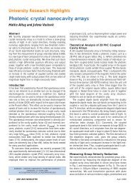
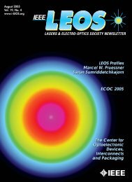
Page 22, Fig. 3. Intensity and phase responses <strong>of</strong> anembedded ring resonator with an odd mode numberdifference. It exhibits an EIT-like pr<strong>of</strong>ile at the‘through’ port, with half <strong>of</strong> the outer ring is lightened.<strong>IEEE</strong>NEWSTHE SOCIETY FOR PHOTONICS<strong>Dec</strong>ember 2008 Volume 22, Number 6FEATURESResearch Highlight: ........................................................................ 4“How to bring Nanphotonics to application – Silicon Phontonics packaging,”by L. Zimmermann, T. Tekin, H. Schroede, P. Dumon, and W. BogaertsDEPARTMENTS4News .................................................... 16• Call for Nominations–– 2009 <strong>IEEE</strong>/LEOS Award Reminders:- Quantum Electronics Award,and Distinguished Lecturer Awards–– 2009 <strong>IEEE</strong>/LEOS Awards:- William Streifer Scientific AchievementAward, Engineering Achievement Award, Aron Kressel Award,and Distinguished Service Award–– <strong>IEEE</strong> <strong>Photonics</strong> Award–– <strong>IEEE</strong> Fellows• Nomination Forms• Article by winner <strong>of</strong> LEOS Figure Contest –“Embedded Ring Resonators”Careers .................................................. 23• John Tyndall Award Recipient: Joe C. Campbell122125Membership .............................................. 24• Benefits <strong>of</strong> <strong>IEEE</strong> Senior Membership• New Senior Members• Chapter Highlight – Taipei Chapter• Book Review – “<strong>Photonics</strong> Signal Processing:Techniques and Applications,” by Le Nguyen BinhConferences. ............................................. 28• <strong>IEEE</strong>/LEOS Winter Topicals - 2009• The Optical Data Storage Topical Meeting - 2009• 20th Annual Workshop on Interconnections Within High SpeedDigital Systems – 2009• IPRM - 2009• <strong>IEEE</strong>/LEOS International Conference on Optical MEMS& Nanophotonics - 2009Publications .............................................. 33• Call for Papers:–– <strong>IEEE</strong>/Journal <strong>of</strong> Selected Topics in Quantum Electronics (JSTQE)–– <strong>IEEE</strong>/OSA Journal <strong>of</strong> Lightwave Technology (JLT)–– <strong>IEEE</strong>/OSA Journal <strong>of</strong> Display Technology (JDT)COLUMNSEditor’s Column. .......... 2 President’s Column . . . . . . . . . . . 3<strong>Dec</strong>ember 2008 <strong>IEEE</strong> LEOS NEWSLETTER 1
Editor’sColumn<strong>IEEE</strong> Lasers andElectro-Optics <strong>Society</strong>Krishnan Parameswaran<strong>Dec</strong>ember marks the end <strong>of</strong> another successful yearfor LEOS. This month, we have a feature article by LarsZimmermann and colleagues at Technische UniversitaetBerlin on packaging <strong>of</strong> nanophotonics, an importanttopic for future applications development.We also have a nice summary <strong>of</strong> activities in the Taiwanchapter by Pr<strong>of</strong>. Ching-Fuh Lin <strong>of</strong> National TaiwanUniversity, describing the variety <strong>of</strong> photonics researchactivities there. We are happy to present our first bookreview by Pr<strong>of</strong>. José Azaña <strong>of</strong> the Institut National dela Recherche Scientifique (INRS) in Montréal, Canada. Iam sure that readers will find this review to be informative,and I hope that you will encourage more reviews infuture.I am also happy to announce the winner <strong>of</strong> the firstLEOS Figure Contest. Lin Zhang <strong>of</strong> the University <strong>of</strong>Southern California has written a nice article in this issueabout the work behind his winning figure showing thefield pattern in an embedded ring resonator. His figureis on the cover <strong>of</strong> this issue. Look for it in future LEOSpublicity.I write this column the week following the 21st LEOSAnnual Meeting held in Newport Beach, California. Iwas happy to meet many <strong>of</strong> you there, and hope to presentsome meeting highlights in our February issue.I wish you all a happy conclusion to 2008 and lookforward to hearing from you in future!Krishnan ParameswaranPresidentJohn H. MarshIntense, Ltd.4 Stanley BoulevardHamilton International Tech ParkBlantyre GlasgowG72 0BN Scotland, UKTel: +44 1698 772 037Fax: +44 1698 827 262Email: j.h.marsh@ieee.orgSecretary-TreasurerFilbert BartoliLehigh University19 West Memorial DrivePackard Lab 302Bethlehem, PA 18015Tel: +1 610 758 4069Fax: +1 610 758 6279Email: fbartoli@lehigh.edu; fjb205@lehigh.eduPast-PresidentAlan WillnerUniversity <strong>of</strong> Southern CaliforniaDept. <strong>of</strong> EE-Systems/ Rm EEB 538Los Angeles, CA 90089-2565Tel: +1 213 740 4664Fax: +1 213 740 8729Email: a.willner@ieee.orgExecutive DirectorRichard Linke<strong>IEEE</strong>/LEOS445 Hoes LanePiscataway, NJ 08855-1331Tel: +1 732 562 3891Fax: +1 732 562 8434Email: r.linke@ieee.orgBoard <strong>of</strong> GovernorsM. Amann H. KuwaharaK. Choquette C. MenoniC. Gmachl J. MeyerK. Hotate D. PlantJ. Jackel A. SeedsT. Koonen P. WinzerVice PresidentsConferences – E. GolovchenkoFinance & Administration – S. NewtonMembership & Regional Activities- A. HelmyPublications – C. MenoniTechnical Affairs – A. SeedsNewsletter StaffExecutive EditorKrishnan R. ParameswaranPhysical Sciences Inc.20 New England Business CenterAndover, MA 01810Tel: +1 978 738 8187Email: krp@psicorp.comAssociate Editor <strong>of</strong> Asia & PacificHon TsangDept. <strong>of</strong> Electronic EngineeringThe Chinese University <strong>of</strong> Hong KongShatin, Hong KongTel: +852 260 98254Fax: +852 260 35558Email: hktsang@ee.cuhk.edu.hkAssociate Editor <strong>of</strong> CanadaLawrence R. ChenDepartment <strong>of</strong> Electrical &Computer EngineeringMcConnell Engineering Building,Rm 633McGill University3480 University St.Montreal, QuebecCanada H3A-2A7Tel: +514 398 1879Fax: 514-398-3127Email: lawrence.chen@mcgill.caAssociate Editor <strong>of</strong> Europe/Mid East/AfricaKevin A. WilliamsEindhoven University <strong>of</strong> TechnologyInter-University Research InstituteCOBRA on CommunicationTechnologyDepartment <strong>of</strong> Electrical EngineeringPO Box 5135600 MB Eindhoven, The NetherlandsEmail: K.A.Williams@tue.nlStaff EditorGiselle Blandin<strong>IEEE</strong>/LEOS445 Hoes LanePiscataway, NJ 08855-1331Tel: +1 732 981 3405Fax: +1 732 562 8434Email: g.blandin@ieee.orgLEOS Newsletter is published bimonthly by the Lasers and Electro-Optics <strong>Society</strong> <strong>of</strong> the Institute <strong>of</strong> Electrical and ElectronicsEngineers, Inc., Corporate Office: 3 Park Avenue, 17th Floor, NewYork, NY 10017-2394. Printed in the USA. One dollar per memberper year is included in the <strong>Society</strong> fee for each member <strong>of</strong> theLasers and Electro-Optics <strong>Society</strong>. Periodicals postage paid atNew York, NY and at additional mailing <strong>of</strong>fices. Postmaster: Sendaddress changes to LEOS Newsletter, <strong>IEEE</strong>, 445 Hoes Lane,Piscataway, NJ 08854.Copyright © 2008 by <strong>IEEE</strong>: Permission to copy without fee all orpart <strong>of</strong> any material without a copyright notice is granted providedthat the copies are not made or distributed for direct commercialadvantage, and the title <strong>of</strong> the publication and its dateappear on each copy. To copy material with a copyright noticerequires specific permission. Please direct all inquiries or requeststo <strong>IEEE</strong> Copyrights Office.2 <strong>IEEE</strong> LEOS NEWSLETTER <strong>Dec</strong>ember 2008
President’sColumnJohn H. MarshA review <strong>of</strong> the yearWriting this column is a difficult balancing act from a timingperspective. In order to meet the publication schedule, Ihave to write the content several weeks before the month inwhich LEOS News is printed. For many members, includingme, it can then take several months before the postal systemdelivers the final printed document through the door. Underthese circumstances it is difficult to be topical! The time delaycauses particular issues when the deadline is just before one <strong>of</strong>the <strong>Society</strong>’s two major administrative meetings, which is thecase this year.However, it is appropriate to review activity through2008 in the <strong>Dec</strong>ember issue <strong>of</strong> LEOS News, because it isboth the end <strong>of</strong> the year and the half-way point in my twoyearterm as President. The reality is I have to write thecolumn before our Annual Meeting takes place in the secondweek <strong>of</strong> November where important decisions will bemade. Moreover, the Technical Activities Board <strong>of</strong> <strong>IEEE</strong>meets later in the same week and may make significantdecisions that affect the <strong>Society</strong>.Despite these caveats, I can already say 2008 has beena very exciting year for LEOS. One <strong>of</strong> my key goals was todevelop a long term strategy for the <strong>Society</strong> and use this asa framework to detailed objectives. This may sound a verydry goal to have as a central objective, but I believe it is vitalto have alignment across the different vice-presidentialareas if the <strong>Society</strong> is to function effectively and consistently.In most organizations, the <strong>of</strong>ficers meet frequentlyas a group and also in sub-groups. In LEOS, however, theBoard <strong>of</strong> Governors only meets twice a year with one additionalstrategy planning workshop attended by the Vice-Presidents, so a clear strategy is vital.A major external influence on the <strong>Society</strong> is the economicenvironment, which could hardly be described asgood. Even before the spectacular failures <strong>of</strong> the bankingindustry, the photonics sector was not financially strong.The reasons for this are many, with over capacity still inthe system from the communications bubble and a myriad<strong>of</strong> small and medium sized companies producing similarproducts. The manifestation <strong>of</strong> the problem is pr<strong>of</strong>itability–with a few notable exceptions companies in the photonicssector were simply not generating reasonable pr<strong>of</strong>itseven before the crisis. As a result, many major photonicscompanies had market capitalizations close to, or below,their annual turnover. The current fall in share prices ismaking this situation even worse, and it will be difficultin the short term for the photonics sector to attract the financialinvestment which is suddenly in very short supply.Also, given the enormous levels <strong>of</strong> support that have beenrequired by banks, I believe it is inevitable that governmentinvestment in technology will slow down. Furthermore,there is a high risk that inflation will devalue whatgovernment investment there is. A period <strong>of</strong> consolidationseems inevitable.On the positive side, photonics is ever more pervasive inelectronic products <strong>of</strong> all types, and the medium and longterm future <strong>of</strong> our industry is secure. Many market areasare experiencing growth including:• Communications, particularly the access market• Displays <strong>of</strong> all kinds, including conventional flat panelsbased on new materials, projection displays rangingfrom pico-projectors through to digital cinema, anddevelopments in 3-D technology• Industrial lasers, where fiber is displacing other lasersystems and making inroads into conventional weldingand cutting technologies• Medical and biophotonic products encompassing lasersurgery, photodynamic therapy, diagnostics rangingfrom imaging to gene sequencing and consumer productsfor cosmetic useRetaininghooks tohold coildown(continued on page 15)63mm, 101mm and304mm Spool DiametersFiber Coil Stack PacksPress-fitprotectionforconnectors<strong>Dec</strong>ember 2008 <strong>IEEE</strong> LEOS NEWSLETTER 3
Research HighlightsHow to bring nanophotonics to application– silicon photonics packagingL. Zimmermann, T. Tekin, H. Schroeder, P. Dumon, and W. BogaertsLars Zimmermann is with Technische Universitaet Berlin,HFT 4, Einsteinufer 25, 10587 Berlin, GERMANYTolga Tekin is with Technische Universitaet Berlin,TIB 4/2-1, Gustav-Meyer-Allee 25, 13355 Berlin, GERMANYHenning Schroeder is with Fraunh<strong>of</strong>er Institute for Reliabilityand Microintegration (IZM),G.-Meyer-Allee 25, 13355 Berlin, GERMANYPieter Dumon is with Ghent University - IMEC, dept. <strong>of</strong>Information Technology (INTEC), <strong>Photonics</strong> ResearchGroup. Sint-Pietersnieuwstraat 41, 9000 Gent, BELGIUMWim Bogaerts is with Ghent University - IMEC, dept. <strong>of</strong>Information Technology (INTEC), <strong>Photonics</strong> ResearchGroup. Sint-Pietersnieuwstraat 41, 9000 Gent, BELGIUMAbstract: Fiber pigtailing and packaging <strong>of</strong> nanowaveguide circuitsare key technologies to realize nanophotonic applications. Technicalproblems start with a large mode mismatch <strong>of</strong> nanowires andstandard single-mode fibers, which requires innovative couplingstructures for low coupling loss and for large alignment tolerances.Looking further ahead, solutions are needed that allow for waferlevel optical device testing and also for reduced packaging costs.These are essential ingredients for making nanophotonics a trulycompetitive and large scale technology. In the following we shallpresent work that focuses exactly on such issues, covering a generalevaluation <strong>of</strong> coupling techniques, silicon grating couplers, fiber arraypackaging <strong>of</strong> silicon nanophotonic circuits, and roads to reducedcosts and generic nanophotonic packaging.1. IntroductionSilicon photonics based on silicon-on-insulator (SOI) nanophotonicwaveguides is a promising technology for integratedphotonics due to unique properties <strong>of</strong> the ultra-high index contrastsilicon waveguide systems, and due to the use <strong>of</strong> advancedmicroelectronics manufacturing technologies. The high indexcontrast <strong>of</strong> silicon nanowires allows for sharp waveguide bendswith radii <strong>of</strong> just a few microns [Bogaerts_JLT05]. The footprint<strong>of</strong> silicon nanowaveguide devices is therefore stronglyreduced compared to classical integrated optics. Still, a sufficientlylarge fraction <strong>of</strong> the guided light <strong>of</strong> nanowires is outside<strong>of</strong> the waveguide core in the evanescent field, making suchwaveguide structures also very promising candidates for sensingapplications [DensmoreA_PTL06]. Furthermore, the exploitation<strong>of</strong> nonlinear properties <strong>of</strong> silicon in nanowaveguidestructures shows strong potential for use in tele or datacom[Q.Lin_OEx07]. Last but not least, the use <strong>of</strong> common processtools and advanced SOI substrates make silicon nanowires anatural choice for integration with advanced microelectronics.Despite such positive prospects there remains a majorstumbling block on the way to nanophotonics applications -the issue <strong>of</strong> coupling light in and out <strong>of</strong> nanophotonic circuitsby means <strong>of</strong> optical fibers. The major problem stems from thelarge mismatch in modesize <strong>of</strong> nanowires (~ a few hundred3025SMF282.01.81.61.4Silicon nanowire20vertical/mm15vertical/mm1.21.00.80.6100.40.2SiO 250.00.0 0.5 1.0 1.5 2.0 2.5horizontal/mm00 5 10 15 20 25 30horizontal/mmFigure 1. Intensity distributions (modesize) <strong>of</strong> a standard telecom fiber (SMF28) and a silicon nanowire (TE). Note the significant differencein scale. Without modesize adaptation techniques, coupling loss would be in excess <strong>of</strong> -16 dB.4 <strong>IEEE</strong> LEOS NEWSLETTER <strong>Dec</strong>ember 2008
single-mode fiberPolymer coreSi coreadiabatic taperphotonic wireSi taperto integratedcircuitSiO2 under-claddinggrating12 mm wide waveguideFigure 2. Lateral coupler (a) using spotsize conversion via inverse taper (from [Tsuchizawa_JSTQE05]). Vertical coupling via diffractiongrating in the nanowaveguide (b).loss [dB]0−1−2−3−4−1.0−0.5X-direction (TE)Y-direction (TE)0.0displacement [mm]Figure 3. Example <strong>of</strong> fiber-chip coupling penalty for horizontal (X)and vertical (Y) displacement from the optimum position. Couplingbetween a 3 µm nitride box waveguide on SiO 2and a 3 µm fiberspot. Penalty is 1 dB in both directions for a 1D-displacement <strong>of</strong> ±0.5µm. The XY displacement tolerance for a 1 dB penalty is ±0.3 µm.0.51.0nanometers) and standard single mode fibers (SMF, ~ 10 µm),which is illustrated in Figure 1. Various spot-size converters andcoupling schemes between the silicon circuits and fiber havebeen demonstrated, with losses down to below 1dB. However,most complex integrated circuits require a high optical ‘pinout’.Achieving high-yield, low-penalty coupling to arrays <strong>of</strong>fibers is still a challenge today.Many solutions to overcome low efficiency coupling havebeen proposed and new work keeps appearing in literature.They follow in general one <strong>of</strong> the following two approaches:• Lateral coupling (in plane)• Vertical coupling (out <strong>of</strong> plane)Both techniques require spotsize conversion. However, theydiffer in the dimension <strong>of</strong> spotsize conversion, i.e. whether theyjust deploy lateral spot-widening (1D-tapering) or true extension<strong>of</strong> the mode in the second dimension (2D-tapering). Lateralcoupling implies 2D-spotsize conversion. Vertical couplingrequires out <strong>of</strong> plane diffraction via gratings. Both schemes aredepicted in Figure 2. Note that in case <strong>of</strong> nanowaveguide dimensionsreflection is not efficient due to the diffraction limit.Lateral and vertical coupling experiments have demonstratedlow insertion loss. However, besides efficiency, other constraintscan also limit the feasibility <strong>of</strong> a coupling approach.That will be clarified in the following by a brief overview <strong>of</strong>how lateral and grating coupler techniques are put to work.The next section will then provide a more detailed account <strong>of</strong>grating couplers that are certainly the most appealing interfaceto silicon photonics due to their availability in the front-end <strong>of</strong>line (FEOL) and their large modesize. We shall see later on thatgrating couplers are excellent means <strong>of</strong> wafer-level probing andpigtailing with single mode fiber (SMF) arrays.Lateral coupling. Nanowaveguide taper-structures usuallyimply the fabrication <strong>of</strong> a sub-100nm nanotip and precise downtapering to that tip-size. Excellent control <strong>of</strong> critical dimensions(CD) is mandatory with such tapers. Matching the modesize <strong>of</strong>SMF is very difficult to achieve with a single taper structure.Therefore, the nanowaveguide mode is first expanded to an intermediatespotsize <strong>of</strong> ~ 3 µm and launched into a larger waveguideby means <strong>of</strong> the nanotip. The process is also referred to asmode conversion, because the spotsize at the nanotip matchesthe fundamental mode <strong>of</strong> the larger waveguide. In a second taperstage the spotsize is then adapted to SMF. Double taperstructures are sensitive to process variations and quite elaboratein process design and development. Most 2D-tapers are thereforesingle-stage and limited in their modesize to approximately3-4 µm. Efficient coupling to such mode diameters can beachieved by means <strong>of</strong> lensed fibers or high-numerical-aperturefibers (high-NA), but mechanical alignment tolerances remainsubstantially below 1 µm. This is illustrated for the couplingbetween a 3 µm waveguide and a lensed fiber with 3 µm spotsize(Figure 3).Furthermore, tapering in the vertical direction requiresdealing with substantial topography, so taper processing hasits place naturally at the very back-end <strong>of</strong> line (BEOL). Lateralcoupling also requires precise preparation <strong>of</strong> the edge <strong>of</strong> the die,either by polishing (if optically flat surfaces are required) or byprecision grinding (if the distance to the edge <strong>of</strong> the die needs6 <strong>IEEE</strong> LEOS NEWSLETTER <strong>Dec</strong>ember 2008
Accelerating the pace <strong>of</strong> engineering and scienceOver one million people around theworld speak MATLAB.Engineers and scientists in every fieldfrom aerospace and semiconductorsto biotech, financial services, andearth and ocean sciences use it toexpress their ideas.Do you speak MATLAB?Saturn's northern latitudesand the moon Mimas.Image from theCassini-Huygens mission.Related article atmathworks.com/ltc®PHOTO: European Space Agency ©2008 The MathWorks, Inc.The language <strong>of</strong> technical computing
Fiber CorefibercoreθP inP upSilicon (220 nm)ySiO 2 buffer layer (2 mm)0.60.50.4xzpower upfiber 10°fiber 8°reflection(a)n topn = 3.47 220 nmn = 1.441 mmn = 3.47Coupling efficiency0.60.50.40.30.20.1P do(a)50 nm−1dB bandwidthSilicon substrate01475 1525 1575 1625Wavelength (nm)0.3(b)0.20.11500 1550 1600 1650wavelength (nm)(b)Figure 4. Cross section through single etch 1D-grating structurewith non-uniform fill factor (a). Coupling characteristics <strong>of</strong> simpleuniform 1D-grating structure (b). Depicted curves show upwardsradiated power, coupling efficiency to the fiber and reflection at thewaveguide grating interface.10°(a)TETE(b)10 mmFigure 5. A 2D grating couples each <strong>of</strong> the two orthogonal states <strong>of</strong> polarization <strong>of</strong> the incominglight into a separate nanowire, thus implementing polarization diversity (a). Scanningelectron microscope (SEM) image <strong>of</strong> 2D grating coupler with access waveguides (b).Figure 6. Grating coupler with silicon overlay to increase efficiency (a).Measured coupling efficiency <strong>of</strong> a grating coupler with overlay (b).to be critically defined). A considerable process overhead shouldtherefore be kept in mind when lateral coupling is considered.Vertical coupling is achieved by means <strong>of</strong> second ordergrating structures. A more detailed account <strong>of</strong> grating couplerswill follow in the next section. We shall limit this paragraphto a concise review <strong>of</strong> grating coupler properties as requiredfor a first comparison with lateral couplers. The fabrication <strong>of</strong>gratings necessitates precise control over etch depth and etchpr<strong>of</strong>ile. However, grating fabrication is fully compatible withFEOL processing. Gratings essentially act like a filter, exhibitingstrong polarization dependence and limited bandwidth.The peak efficiency <strong>of</strong> simple grating couplersis rather low (-4.5 dB). Strategies havebeen devised and experimentally verifiedthat overcome low efficiency and polarizationdependence, though at the cost <strong>of</strong> additionalprocess effort. Furthermore, gratingcouplers are fabricated by planar wafer-levelprocesses, and do not require single die processing.They provide the capability <strong>of</strong> waferlevel optical probing.A comparison <strong>of</strong> lateral and vertical couplingfrom the point <strong>of</strong> view <strong>of</strong> fiber pigtailingis summarized in Table 1.2. Grating couplersCoupling to silicon photonic wires throughhigh-index contrast gratings is attractivebecause <strong>of</strong> the relaxed alignment tolerancescompared to facet coupling. Grating couplersmatch standard single mode fibers.8 <strong>IEEE</strong> LEOS NEWSLETTER <strong>Dec</strong>ember 2008
Because <strong>of</strong> the high index contrast, the gratingcan be short (25 periods) and achieve arelatively large bandwidth.Simple one-dimensional grating couplerswith a uniform fill factor, etched into a broadwaveguide, achieve a coupling efficiency <strong>of</strong>around 35% (-4.5 dB) with a 40nm 1dB bandwidth(per coupler) for a single polarization.Detuned gratings with a coupling angle <strong>of</strong> 8ºto 10º are used in order to avoid back reflections.The alignment tolerance for a 1dB losspenalty exceeds ±1µm. A schematic cross sectionthrough a 1D-grating coupler structure isshown in Figure 4(a). Figure 4(b) depicts simulatedcoupling characteristics <strong>of</strong> a typical 1Dgrating with uniform fill factor. The total upwardscoupled light exceeds the light coupledto the fiber due to mismatch <strong>of</strong> the respectivefar-field characteristics. There is also an angulardependence <strong>of</strong> the maximum coupling. Theshift <strong>of</strong> the maximum <strong>of</strong> the reflection curvereveals the detuning <strong>of</strong> the grating. 1D gratingsare optimized for TE polarization ([Taillaert06JJAP]).Experimentally measured couplingefficiencies match the simulation results.Coupling loss to SMF(butt fiber)Coupling loss to SMF(lensed fiber, incl. excessloss due to lens)Coupling tolerancesfor 1dB penaltyIn addition, a two-dimensional grating coupler simultaneouslysplits the two incident polarizations ([Taillaert03PTL])and can be used in a polarization diversity scheme, which isschematically illustrated in Figure 5 (a). A real two-dimensionalgrating coupler is shown in Figure 5 (b). Simple 2D couplersLateral−7 dB (single stage)−1.5 dB (double stage)−1.5 dB (best)−3 dB (typical)Vertical±0.3 mm (single stage) ±1.0 mm3 dB bandwidth Broadband 60 nmPolarizationdependenceSuitable for multiplefiber I/OWeakNo (due to smalltolerances)−4.5 dB (standard grating)−1 dB (optimized grating)achieve similar efficiency and bandwidth as one-dimensionalcouplers, but have reduced alignment tolerances in order toachieve polarization independent circuits.The grating couplers can be optimized in various ways toimprove the efficiency or size. Focusing couplers achieve the−Strong (but can be solvedwith 2D grating andpolarization diversityapproach)Table 1. Relevant properties <strong>of</strong> the major fiber coupling techniques to silicon nanowaveguidesYes<strong>Dec</strong>ember 2008 <strong>IEEE</strong> LEOS NEWSLETTER 9
Fiber # 1 2 3 6 7 8Mismatch in y [mm] −2.2 0.8 0.3 0.1 0.0 2.0Mismatch in x [mm] 0.0 4.0 1.7 −2.5 −4.3 0.0Table 2. Measured deviations <strong>of</strong> fiber positions within an eight fiberarray. Only six fibers are included because fibers 4&5 are not usedduring the experiment. 1550nm CW light source (HP81553SM opticalpower (HP81532A)1A2B3CFigure 7. Schematic drawing <strong>of</strong> a grating coupler array designedand fabricated at IMEC. The grating couplers are interconnected bynanowaveguides (red, orange, green). Coupling loss and uniformity<strong>of</strong> the array coupling process can be determined from simple lossmeasurements between fibers 1/8 (AH), 2/7 (BG), and 3/6 (CF).(a)(b)Figure 8. Photograph <strong>of</strong> Silicon on Insulator (SOI) chip (2.5mm x1.7mm) with shortened grating coupler array (a). To illustrate theproportions <strong>of</strong> the coupling arrangement SMF fibers and gratingpitch have been drawn to scale in (b). Nanowaveguides are stillenhanced to increase visibility.6F7G8HTransmission 1AH8 2BG7 3CF61 dB loss penalty at x-axis[mm]1 dB loss penalty at y-axis[mm]3 dB loss penalty at x-axis[mm]3 dB loss penalty at y-axis[mm]Table 3. Summary <strong>of</strong> alignment penalties±1 ±1 ±1.5±2 ±1.5 ±2±2.5 ±2.5 ±2.8±3.5 ±3.5 ±3.5same efficiency on a much smaller footprint, as with the regularcoupler one still has to taper down the broad waveguide [Van-Laere07PTL]. By using non-uniform fill factors, lower couplinglosses can be obtained and the efficiency can be further boostedby decreasing the vertical symmetry <strong>of</strong> the structure or addingbottom mirrors [Taillaert06JJAP]. With an overlay, efficientcouplers can be obtained [Roelkens08APL]. Figure 6 (a) showsa grating with increased efficiency due to a silicon overlay(thickening). Such overlays have been realized by epitaxial overgrowth.The experimentally determined coupling efficiency <strong>of</strong>an overlay grating is plotted in Figure 6 (b). Here, the couplingloss is decreased to -2.5 dB.The main benefit <strong>of</strong> coupling to vertically mounted fibers isfor wafer-scale testing and characterization. By hovering fibersover the on-chip couplers, photonic integrated circuits can betested in much the same way as standard electrical wafer-scaletests are done.3. Fiber array packagingDue to the extended usage <strong>of</strong> different multiplexing techniques,and due to the increase <strong>of</strong> functionalities which are integratedwithin a single photonic integrated circuit (PIC), the number <strong>of</strong>optical ports increases and multiple fiber I/O becomes more andmore important. Today many different commercial fiber arraysolutions are available.Tolerances <strong>of</strong> commercial fiber arrays. Limitations in case <strong>of</strong>commercial fiber arrays are related to their uniformity. Here extensivemeasures can be taken to minimize the tolerances relatedto the dimensions <strong>of</strong> v-shaped grooves for carriers <strong>of</strong> arrayedfibers. However most likely the fiber tolerances especially thevariation within the fiber core and fiber cladding concentricitydefine the uniformity limits. The core-cladding concentricitytolerance is < 0.5 for SMF-28 fiber, so an alignment error below1 per single fiber within a multiple fiber array can be manufactured.However, to understand the tolerances <strong>of</strong> presently availablefiber arrays we investigated the actual alignment precision<strong>of</strong> a purchased fiber array.By using a precise alignment system (PI F206) and a singlemode fiber, the lateral deviations <strong>of</strong> a commercial fiber array (core<strong>of</strong> the fiber) from the ideal position was measured by scanningalong the array with the optical probe and detecting the receivedsignal as a function <strong>of</strong> the lateral position. The deviations <strong>of</strong> the positions<strong>of</strong> the respective fiber cores from the ideal are listed in Table2, which shows that the total deviation from the ideal position10 <strong>IEEE</strong> LEOS NEWSLETTER <strong>Dec</strong>ember 2008
could amount to more than what would be expectedfrom the manufacturer’s specifications.In this particular case the pitch deviated by4 µm from the expected between fiber 1 & 8(distance 1750µm).Fiber array coupling. Recently, we carriedout a study concerning generic fiberarray interconnections for silicon photonics([Tekin08_ECOC]). In course <strong>of</strong> thiswork we investigated the pigtailing penaltywhen coupling a commercially availablefiber array to an SOI chip with an array <strong>of</strong>grating couplers. The SOI chip was manufacturedfor testing purposes at IMEC andcarried 6 spare vertical grating couplerports, which were shortened by nanowaveguides(Figure 7).The sensitivity <strong>of</strong> transmission to thealignment between fiber array and SOI chipwas investigated. The position <strong>of</strong> the SOI chipwas varied and the transmissions through theports AH, BG, and CF were measured, respectively.A photograph <strong>of</strong> the SOI chip is shownin Figure 8 (a). To illustrate the proportionsbetween nanophotonic chip and fiber array, 3fibers have been depicted to scale over the SOIchip in the drawing in Figure 8(b).The measured alignment sensitivity forcoupling between a grating coupler and a SMFis depicted in Figure 9. The key to successfulfiber array coupling is a large alignment toleranceat each individual coupling point. Themeasured alignment tolerance <strong>of</strong> a waveguidegrating coupler for a 1dB loss penalty is ±2µm.The measured sensitivity is summarized in thefollowing Table 3. Hereto, 1 dB and 3 dB losspenalties in the lateral direction are provided.The chip alignment is optimized by activealignment using the monitoring portson the SOI chip. The position (x, y, z, androtation) <strong>of</strong> the SOI chip was varied and thetransmission through the ports AH, BG, andCF was monitored for optimized polarizationstate. After active alignment the chip is fixedby a UV-curing epoxy. The basic assemblyconfiguration is depicted in Figure 10. Nosignificant change in transmission signal wasobserved after the curing process. The genericfiber array based package without andwith glob top encapsulation are depicted inFigure 11 and 12, respectively. The SOI chipis mounted face down on the fiber array.The wavelength dependence <strong>of</strong> the transmissionthrough shortened grating couplerswas measured, where HP8168A was used as anECL (external cavity laser). The transmissioncurves in Figure 13 have a comparable performance,and non-uniformity was ~ 1dB. Wex-axis [mm]1086420−2−4−6−8−10−10 −8 −6 −4 −2 0 2 4 6 8 10y-axis [mm]<strong>Dec</strong>ember 2008 <strong>IEEE</strong> LEOS NEWSLETTER 11−20,00−19,00−18,00−17,00−16,00−15,00−14,00−12,00−12,00−11,00−10,00−9,000−8,000−7,000−6,000−6,000−4,000−3,000−2,000−1,0000Figure 9. Experimentally determined penalty <strong>of</strong> coupling between SMF and standardgrating couplers. A penalty <strong>of</strong>
fibersobserved insertion loss <strong>of</strong> up to approximately-12 dB, with typical shape <strong>of</strong> grating couplerfilter curves. The penalty due to multiple fiberpigtailing therefore amounts to ~ 1-2 dB.globtopSOIchipglassv-groovecarrierFigure 10. Schematic drawing <strong>of</strong> how a fiber array package is assembled. The mechanicalsupport <strong>of</strong> the fibers stems from the v-groove base itself.Figure 11. Photograph <strong>of</strong> the v-groove base with the mounted SOI die.4. Generic packages & outlookAs the optical ‘pin-out’ <strong>of</strong> silicon photonicchips increases, costs <strong>of</strong> optical fiber alignmentincrease even stronger. Therefore, for researchand testing purposes, costs can be reduced toan affordable level only by standardization.Such is possible with a generic fiber pigtailingapproach and a generic package for prototyping,by which the non-recurring costs can bespread over a large number <strong>of</strong> users. In thisapproach, the chip design is adapted to thepackage, rather than the other way round.In that case, when IC designers make sureto keep to some fixed design rules for the placement and configuration<strong>of</strong> on-chip optical fiber couplers, the resulting chipscan be pigtailed and packaged at much reduced cost.In addition, silicon photonic IC’s are going to get electricalcontacts. A generic package approach for prototyping shouldtherefore handle both optical and electrical pin-out.Within the EU-funded ePIXnet Network <strong>of</strong> Excellence onphotonic integration, the authors are working on such a genericpackage approach under the name <strong>of</strong> g-Pack. This work is collaborationbetween ePIXpack ([ePIXpack]), the packaging serviceplatform, and ePIXfab ([ePIXfab]), the silicon photonic ICprototyping service. Both services were set up within ePIXnet.As a result, ePIXfab users will be able to have a number <strong>of</strong> theirchips fiber pigtailed and packaged through ePIXpack for testingpurposes. For low-frequency electrical I/O, the engineering costis relatively small. Therefore, we focus first on the combination<strong>of</strong> optical fiber connections with DC or low-frequency (~1MHz)electrical contacts, such as for thermo-optic tuners or for switch-transmission [dB]0−5−10−15−20path 1AH8path 2BG7path 3CF6−251520 1530 1540 1550 1560 1570wavelength [nm]Figure 12. Photograph <strong>of</strong> the final fiber array package with globtopprotection. The solution is very compact due to the small scale <strong>of</strong>the nanophotonic die.Figures 13. Transmission characteristics as measured on the fiberarray package. Bandwidth is reduced due to the coupling via 2 gratings.Minimum loss <strong>of</strong> the couplers would be -9 dB, so a maximumpenalty <strong>of</strong> 2 dB is incurred by fiber array pigtailing process. Uniformityis ± 1 dB.12 <strong>IEEE</strong> LEOS NEWSLETTER <strong>Dec</strong>ember 2008
Stay Connected with <strong>IEEE</strong>We know you work hard to get where you’re going and that <strong>IEEE</strong> membership isessential to your career. Renew your membership for 2009 and stay connectedto valuable benefits and services to help advance your career. No matter what yourinterests are—<strong>IEEE</strong> membership provides benefits to help you go further.<strong>IEEE</strong> memberNetBuild your pr<strong>of</strong>essional network withthe only online web site that connects<strong>IEEE</strong> members across the globe.www.ieee.org/membernet<strong>IEEE</strong>.tvAccess exclusive, special-interestprogramming in a variety <strong>of</strong> engineeringand technology fi elds.www.ieee.org/ieeetv<strong>IEEE</strong> Mentoring ConnectionInitiate a partnership with another <strong>IEEE</strong>member to gain experience and insight.www.ieee.org/mentoring31 <strong>Dec</strong>ember is the end <strong>of</strong> the membership year.Don’t let your <strong>IEEE</strong> benefi ts expire—Renew Today!www.ieee.org/renew<strong>IEEE</strong> Membership: Connecting Pr<strong>of</strong>essionals, Advancing Technology
es. In a later stage, an extension to RF is possible, for instancewith a co-planar 50W non-impedance matched approach.g-Pack is designed for vertical fiber couplers, with a fiberarray up to 32 fibers. A first example with an eight fiber arrayis presently being elaborated ([Zimmermann08_GFP]).The schematic sideview is shown in Figure 14. The g-Pack approachmakes use only <strong>of</strong> commercially available componentssuch as the fiber array and the ceramic pin grid array carrier.The design matches a standardized SOI chip as manufacturedby ePIXfab. All optical I/O is mounted along one side <strong>of</strong> thechip (West), whereas the electrical I/O pads are on the Northand South sides, allowing for up to 65 pins. The topview <strong>of</strong> theg-Pack configuration is shown in Figure 15.The work presented here has resulted from cooperationswithin the European Network <strong>of</strong> Excellence ePIXnet. The workwill continue in the framework <strong>of</strong> the European funded integratedproject HELIOS ([HELIOS]).Figure 14. g-Pack, side view. The pin grid array carrier was chosento provide a large number <strong>of</strong> DC connects & to comply with standardsocket dimensions.connectorsglassblock V-groovecarrierstandardfiberarrayceramicPGAcarrierePlXFab10 × 14 mm 2chipstandard w/w wirebondsFigure 15. g-Pack, top view. The ePIXFab chip is optically coupledto a commercial fiber array (up to 32 fibers), while electrical connectionsare established via standard wire bonding techniques.References1. [Bogaerts_05JLT] Wim Bogaerts, Roel Baets, PieterDumon, Vincent Wiaux, Stephan Beckx, Dirk Taillaert,Bert Luyssaert, Joris Van Campenhout, Peter Bienstman,and Dries Van Thourhout, “Nanophotonic Waveguidesin Silicon-on-Insulator Fabricated With CMOSTechnology”, Journal Lightwave Technology, 23(1), p.401 (2005)2. [DensmoreA_PTL06] A. Densmore, D.-X. Xu, P. Waldron,S. Janz, P. Cheben, J. Lapointe, A. Delâge, B. Lamontagne,J. H. Schmid, and E. Post, “A Silicon-on-InsulatorPhotonic Wire Based Evanescent Field Sensor”, <strong>Photonics</strong>Technology Letters, 18(23), p. 2520 (2006)3. [Q.Lin_OEx07] Q. Lin, O. J. Painter, and G. P. Agrawal,“Nonlinear optical phenomena in silicon waveguides:Modeling and applications”, Optics Express, 15(25) p.16604 (2007)4. [Tsuchizawa_JSTQE05] Tai Tsuchizawa, Koji Yamada,Hiroshi Fukuda, Toshifumi Watanabe, Jun-ichi Takahashi,Mitsutoshi Takahashi, Tetsufumi Shoji, Emi Tamechika,Sei-ichi Itabashi, and Hir<strong>of</strong>umi Morita, “MicrophotonicsDevices Based on Silicon Micr<strong>of</strong>abrication Technology”,Journal <strong>of</strong> Selected Topics in Quantum Electronics, 11 (1),p. 232 (2005)5. [Roelkens08APL] G. Roelkens, D. Vermeulen, D. VanThourhout, R. Baets, S. Brision, P. Lyan, P. Gautier andJ.-M. Fedeli, “High efficiency diffractive grating couplersfor interfacing a single mode optical fiber with a nanophotonicsilicon-on-insulator waveguide circuit”, AppliedPhysics Letters 92 (13), p. 131101 (2008)6. [VanLaere07PTL] F. Van Laere, T. Claes, J. Schrauwen,S. Scheerlinck, W. Bogaerts, D. Taillaert, L. O’Faolain,D. Van Thourhout, R. Baets, Compact Focusing GratingCouplers for Silicon-on-Insulator Integrated Circuits, <strong>Photonics</strong>Technology Letters, 19(23), p.1919-1921 (2007)7. [Taillaert06JJAP] D. Taillaert, F. Van Laere, M. Ayre,W. Bogaerts, D. Van Thourhout, P. Bienstman, R. Baets,Grating Couplers for Coupling between Optical Fibers andNanophotonic Waveguides,Japanese Journal <strong>of</strong> AppliedPhysics (invited), 45(8A), p.6071-6077 (2006)8. [Taillaert03PTL] D. Taillaert, H. Chong, P. Borel, L.Frandsen, R.M. De La Rue, R. Baets, A compact two-dimensionalgrating coupler used as a polarization splitter,<strong>IEEE</strong> <strong>Photonics</strong> Technology Letters, 15(9), p.1249-1251(2003)9. [Tekin08_ECOC] T. Tekin, H. Schröder, L. Zimmermann,P. Dumon, W. Bogaerts, Fibre-Array Optical Interconnectionfor Silicon <strong>Photonics</strong>, Proc. ECOC, Vol. 5, p. 93(P.2.21), Brussels, Belgium (2008)10. [Zimmermann08_GFP] L. Zimmermann, H. Schröder, T.Tekin, W. Bogaerts, P. Dumon, g-Pack – a generic testbedpackage for Silicon photonics devices, Proc. 5th <strong>IEEE</strong> InternationalConference Group IV <strong>Photonics</strong>, p. 371, Sorrento,Italy (2008)11. [ePIXfab] www.epixfab.eu12. [ePIXpack] www.epixpack.eu13. [HELIOS] www.helios-project.eu14. Lars.Zimmermann@tu-berlin.de14 <strong>IEEE</strong> LEOS NEWSLETTER <strong>Dec</strong>ember 2008
President’s Column(continued from page 3)• Military applications• Green technologies, in particular solid state lightingand photovoltaics.LEOS has a vital role in supporting the community throughthis period <strong>of</strong> economic uncertainty and changing technologicalpriorities. The role <strong>of</strong> the <strong>Society</strong> is to serve itsmembers, by being a meeting place, a forum for exchange<strong>of</strong> ideas and a repository for intellectual property. In orderto do this, LEOS needs to adapt continuously to itsmembers’ needs and considerable progress has been madethroughout 2008.Achievements in 2008I would like to highlight a few <strong>of</strong> the <strong>Society</strong>’s achievementsagainst this background – and I would emphasizethat this list is a personal selection.The membership area was restructured at the start <strong>of</strong>2008, with three geographical VPs being replaced by asingle VP responsible for Membership and Regional Activities.The Vice President is now supported by AssociateVPs with responsibility for developing activities in differentgeographical regions and this flexible approach isstarting to produce tangible results. One <strong>of</strong> my personalobjectives was to stabilize LEOS membership and I ampleased to report this has been achieved. Moreover, newchapters have been formed in India, China, North Americaand South America. LEOS News and the web portal alsobecame the responsibility <strong>of</strong> VP Membership and redevelopment<strong>of</strong> the LEOS Portal is currently a key activity.Membership growth in China, India and South Americais being targeted by working closely with conferences.In China, LEOS is working closely with OSA and SPIE toalign and consolidate AOE and APOC. The Summer Topicalswere held in Mexico and LEOS was a co-sponsor <strong>of</strong> the<strong>Photonics</strong> 2008 Conference in India. As part <strong>of</strong> our commitmentto globalization, the first Winter Topical Serieswas held in Italy.I discussed the developments in Publications in somedetail in the August newsletter. During 2009 the <strong>IEEE</strong><strong>Photonics</strong> Journal will be launched – the first on-line onlyjournal in <strong>IEEE</strong>. With multimedia content and broad coverage<strong>of</strong> the photonics field, this will be a particularly excitingdevelopment.In Technical Affairs, the Technical Committee structureis being reviewed, to ensure adequate coverage <strong>of</strong>new topic areas and to support the needs <strong>of</strong> the AnnualMeeting. There have been significant activities in biophotonicsand photovoltaics, with a summer topicalon Advanced Nanobiophotonics, a 2-day EMBS-LEOSSymposium on Advanced Biophotonic Diagnostics andTherapeutics held as part <strong>of</strong> the EMBS Annual Meetingand a photovoltaics symposium within the LEOS AnnualMeeting.Financial performance throughout 2008 has been strong,with conference budgets subjected to thorough review. Theyear has also seen the formation <strong>of</strong> strategic committees:• The Meetings Committee has been reactivated toreview all LEOS meetings, recommend new topic areasand provide guidance to meeting organizers.• A Publications Board has been formed to assess andguide publications in terms <strong>of</strong> quality timeliness andcoverage, assist with selection and recruitment <strong>of</strong> editorialpersonnel, review the need for new and existingpublications and monitor financial performance• A Portal Committee has been formed to develop theweb site• A Technical Affairs Strategy Committee is beingformed to review strengths and weaknesses, to identifyareas <strong>of</strong> growth and to recommend actions that will assistgrowth in LEOS activities in those areasGiven that photonics is an enabling technology for mostelectronic products and systems, it seems logical we shouldbe co-operating with other societies, and indeed LEOS hasworked closely with several <strong>IEEE</strong> Societies and OSA formany years. New developments in 2008 include:• Coordinated conference activities in China with OSAand SPIE• New outreach activities with SPIE• Technical Co-sponsorship <strong>of</strong> the 2009 <strong>IEEE</strong> PhotovoltaicsSpecialists Conference sponsored by the ElectronDevices <strong>Society</strong>• LEOS membership <strong>of</strong> the newly created <strong>IEEE</strong> BiometricsCouncil• The LEOS sponsored symposium, highlighted above,within the EMBS Annual Meeting• Technical co-sponsorship <strong>of</strong> the LEOS <strong>Photonics</strong>Journal by a growing number <strong>of</strong> <strong>IEEE</strong> societies andcouncils.And finally thanksI would like to conclude by saying again that it is a privilegeto be LEOS President, and thanks are due to my employersIntense Ltd and the University <strong>of</strong> Glasgow for enablingme to take this on. I would like to thank LEOS membersfor their outstanding support <strong>of</strong> the <strong>Society</strong> throughout theyear, particularly all the volunteers who serve our Chapters,Conferences, Technical Committees and Publications. Mypersonal thanks go to Katya Golovchenko and Steve Newtonwho retire as Vice-Presidents, and Marcus Amann, Kent Choquette,Hideo Kuwahara and Carmen Menoni who retire aselected BoG members (though Carmen continues as a Vice-President). Finally, on behalf <strong>of</strong> the entire LEOS membership,I would like to thank our 18 staff – Rich Linke, Gail Walters,Christine Bluhm, Linda Matarazzo and their teams – whomake it possible for LEOS volunteers to achieve so much.<strong>Dec</strong>ember 2008 <strong>IEEE</strong> LEOS NEWSLETTER 15
News (cont’d)<strong>IEEE</strong>/LEOSAron Kressel AwardThe Aron Kressel Award is given torecognize those individuals who havemade important contributions to opto-electronicdevice technology. Thedevice technology cited is to have hada significant impact on their applicationsin major practical systems. Theintent is to recognize key contributorsto the field for developments <strong>of</strong> criticalcomponents, which lead to the development<strong>of</strong> systems enabling majornew services or capabilities. Theseachievements should have been accomplishedin a prior time frame sufficientto permit evaluation <strong>of</strong> theirlasting impact. The work cited couldhave appeared in the form <strong>of</strong> publications,patents products, or simplygeneral recognition by the pr<strong>of</strong>essionalcommunity that the individualcited is the agreed upon originator <strong>of</strong>the advance upon which the awarddecision is based. The award maybe given to an individual or group,up to three in number. The awardis administered by the Aron KresselAwards Committee and presented atthe LEOS Annual Meeting.<strong>IEEE</strong>/LEOSDistinguished Service AwardThe Distinguished Service Awardwas established to recognize an exceptionalindividual contribution <strong>of</strong>service that has had significant benefitto the membership <strong>of</strong> the <strong>IEEE</strong>Lasers and Electro-Optics <strong>Society</strong>as a whole. This level <strong>of</strong> service will<strong>of</strong>ten include serving the <strong>Society</strong> inseveral capacities or in positions <strong>of</strong>significant responsibility. Candidatesshould be members <strong>of</strong> LEOS. Theaward is administered by a committeeconsisting <strong>of</strong> the President-Elect,Chair; two Past Presidents, and theVice President <strong>of</strong> Finance & Administrationand is presented at the LEOSAnnual Meeting.A list <strong>of</strong> previous winners and awardsinformation can be found on the LEOSHome Page at www.i-LEOS.org.Call for <strong>IEEE</strong> <strong>Photonics</strong> Award NominationsThe <strong>IEEE</strong> <strong>Photonics</strong> Award is presentedfor outstanding achievementsin photonics. The recipient <strong>of</strong> theaward receives a bronze medal, certificate,and cash honorarium. The nominationdeadline is 31 January 2009.For nomination forms, visit the <strong>IEEE</strong>Awards Web Site, www.ieee.org/awards, or contact <strong>IEEE</strong> Awards Activities,445 Hoes Lane, Piscataway,NJ, USA, 08855-1331; tel: +1 732562 3844; email: awards@ieee.org.Call for Fellow NominationsOn the Lookout fora Few Good Fellowsby Rosann MarosyIt’s not too early to nominate an<strong>IEEE</strong> senior member for the Fellowclass <strong>of</strong> 2010. The deadline is 1March 2009.This prestigious group now numbers6000 out <strong>of</strong> <strong>IEEE</strong>’s total <strong>of</strong> 375 000members. While many view Fellows asvisionaries, pioneers, technology leaders,or influential business executives, youprobably know them as your friends orcolleagues. So take the time to nominatesomeone you know in one <strong>of</strong> four Fellowcategories: application engineer, educator,research engineer, or technical leader.To submit a nomination or learn moreabout these categories and the FellowProgram, visit the Fellow Web site athttp://www.ieee.org/fellows“Nick” Cartoon Series by Christopher Doerr<strong>Dec</strong>ember 2008 <strong>IEEE</strong> LEOS NEWSLETTER 17
News (cont’d)18 <strong>IEEE</strong> LEOS NEWSLETTER <strong>Dec</strong>ember 2008
News (cont’d)<strong>Dec</strong>ember 2008 <strong>IEEE</strong> LEOS NEWSLETTER 19
News (cont’d)20 <strong>IEEE</strong> LEOS NEWSLETTER <strong>Dec</strong>ember 2008
News (cont’d)Embedded Ring ResonatorsLin Zhang, Muping Song, Raymond G. Beausoleil and Alan E. WillnerL. Zhang, and A. E. Willner are with the Dept. <strong>of</strong> ElectricalEngineering, Univ. <strong>of</strong> Southern California, CA 90089, USA(e-mail: linzhang@usc.edu).M. Song is with Dept. <strong>of</strong> Information and ElectronicEngineering, Zhejiang Univ., 310027, China.R. G. Beausoleil is with the HP Labs, Palo Alto, CA 94304, USA.IntroductionThe Winner <strong>of</strong> the Inaugural LEOS Figure Contest is LinZhang <strong>of</strong> the University <strong>of</strong> Southern California. His figureshowing the simulated field distribution in an embeddedring resonator is on this month’s cover and willbe used in LEOS publicity. He has written the articlebelow describing the work behind it. Look for this imagein future LEOS publications!(a)(b)Microscale optical resonators have become quite popularstructures for achieving versatile functional devices in asmall surface area. Resonators can enable lasers, modulators,filters, delay elements, and sensors, where resonanceenhancedoperation efficiently achieves compact chipsize, low power consumption, reduced group velocity andhigh sensitivity. In recent years, the family <strong>of</strong> the microresonatorshas grown to include micro-disk, micro-ring,micro-sphere, micro-toroid, micro-coil, and micro-spiralresonators. More advanced functionality can be enabledby cascading these resonators in serial,parallel, or coiled configurations.An intriguing modification has beento explore the performance <strong>of</strong> resonatorsin an “embedded” structure.These embedded ring resonators(ERRs) could potentially enable newtypes <strong>of</strong> on-chip photonic elements[1]. The figure that we submitted tothe LEOS Figure Contest is a simulatedoptical mode distribution inan ERR, and the plot <strong>of</strong> the modedistribution was helpful in our understanding<strong>of</strong> the operation <strong>of</strong> suchstructures.Figure 1 shows various ring-resonatorstructures that are coupled totwo waveguides. The coupling betweenthe embedded ring resonatorscan be in a distributed or a point-topointmanner (Fig. 1(c,d)). Each resonatorcan have its own mode numberIntensity (dB)(c)Fig. 1. (a,b) Conventional single-ring and coupled-ring resonators;(c,d) Embedded ring resonators with distributed andpoint-to-point coupling, respectively.m, satisfying nL i=mil Ri, where L iis the perimeter <strong>of</strong> the i thring, and n is the effective refractive index <strong>of</strong> a travelingoptical wave at wavelength l Ri, and the mode number miis the number <strong>of</strong> optical cycles that exist in the ring. For aWavelengthdrop drop dropin0−60−120l 1 l 2 l 3 l 1 l 2 l53throughinthroughin(d)Wavelengththroughat wavelength l 1 at wavelength l 2 at wavelength l 2Fig. 2. Intensity and phase responses <strong>of</strong> an embedded ring resonator with an even modenumber difference. It exhibits a doublet at the ‘drop’ port, corresponding to symmetricand anti-symmetric modes in the steady-state mode distributions.Phase (rad)31<strong>Dec</strong>ember 2008 <strong>IEEE</strong> LEOS NEWSLETTER 21
News (cont’d)Intensity (dB)Phase (rad)0−10−20630l 4Wavelengthdropinat wavelength l 4throughAcknowledgementThe authors thank Ling Lu and Pr<strong>of</strong>.M.-J. Chu for helpful discussions.This work is generously supported byHP Labs.References[1] L. Zhang, M. Song, T. Wu, L.Zou, R. G. Beausoleil and A. E.Willner, “Embedded ring resonatorsfor micro-photonic applications,”Optics Letters, vol. 33, no.17, pp. 1978-1980, Sep. 2008.Fig. 3. Intensity and phase responses <strong>of</strong> an embedded ring resonator with an odd modenumber difference. It exhibits an EIT-like pr<strong>of</strong>ile at the ‘through’ port, with half <strong>of</strong> theouter ring is lightened.double-ring ERR with point-to-point coupling (Fig. 1(d)),the two rings interact via 2-by-2 couplers at two locations.When the two rings have aligned resonance wavelengths,the phase difference that optical waves experience whentraveling from one coupler to the other depends on the relationship<strong>of</strong> the outer and inner mode numbers (m 1and m 2).There are two operating conditions: one features a spectraltransmission doublet when m 1_m 2is even, while the otherexhibits an electromagnetically induced transparency (EIT)-like pr<strong>of</strong>ile when m 1_m 2is odd.In the even-mode-number case, the two rings have acommon resonance wavelength l 2. When they are embeddedtogether, two resonance peaks are equally shifted froml 2to l 1and l 3in the spectral response at the ‘drop’ port(Fig. 2). These peaks correspond to symmetric and antisymmetricmodes formed in the two couplers, as illustratedby the steady-state mode distributions. There is also a deepnotch at wavelength l 2. In this case, a relatively weak fieldis built in the inner ring, which destructively interferes withthe optical wave traveling over the outer ring, resulting in aneffective cancellation <strong>of</strong> the optical wave at the ‘drop’ port.In the odd-mode-number case (Fig. 3), an EIT-likeresonance pr<strong>of</strong>ile results from a strong interaction <strong>of</strong> theoptical waves traveling over the two rings. As illustratedby the steady-state mode distribution at wavelength l 4,the inner ring depletes almost all <strong>of</strong> the photons comingfrom the outer ring. A small fraction <strong>of</strong> input lightescapes from the ‘drop’ port, and thus a ‘transparent’window is induced at the ‘through’ port. A higher photondensity is seen in the inner ring, as compared to thedoublet case. The optical mode distribution reveals somevery interesting phenomena that remain to be explored.BiographyLin Zhang received his B.S. and M.S.with honors from Tsinghua Univ.,China. He is pursuing the Ph.D. degreeat USC. He has 60 peer-reviewedjournal and conference papers. He was cited as one <strong>of</strong> the2003 Top-Ten Outstanding Graduate Students at TsinghuaUniversity. Mr. Zhang received the 2008 Best Research PaperAward from the Dept. <strong>of</strong> EE at USC and the 2008 <strong>IEEE</strong>LEOS Graduate Student Fellowship.Muping Song received B.S. and Ph.D with honors fromZhejiang Univ., China. He is an associate pr<strong>of</strong>essor <strong>of</strong> theDept. <strong>of</strong> Information and Electronic Engineering at ZhejiangUniv. His research includes microring-based devicesand fiber sensors. He has published >30 peer-reviewed journaland conference papers.Ray Beausoleil is a Distinguished Scientist in theInformation and Quantum Systems Laboratory at HPLabs. He received a B.S. from Caltech and the Ph.D. degreefrom Stanford University. At HP Labs, he performsbasic research in microscale and nanoscale quantum optics.He is a member <strong>of</strong> the affiliate faculty at StanfordUniversity. He has published over 80 papers and conferenceproceedings, five book chapters, and over twodozen patents issued.Alan Willner (F-<strong>IEEE</strong> & F-OSA) is Pr<strong>of</strong>essor <strong>of</strong> EE at USC.He received the NSF Presidential Faculty Fellows Awardfrom the White House, Packard Foundation Fellowship,NSF Young Investigator Award, Fulbright Award, LEOSDistinguished Traveling Lecturer Award, and Eddy PaperAward from Pennwell Publications. He has been President<strong>of</strong> LEOS, Editor-in-Chief <strong>of</strong> <strong>IEEE</strong>/OSA JLT, Editor-in-Chief<strong>of</strong> <strong>IEEE</strong> JSTQE, Editor-in-Chief <strong>of</strong> Optics Letters, and GeneralCo-Chair <strong>of</strong> CLEO.22 <strong>IEEE</strong> LEOS NEWSLETTER <strong>Dec</strong>ember 2008
Career Section2009 John Tyndall Award Recipient:Joe C. CampbellThe John Tyndall Award is jointlysponsored by the <strong>IEEE</strong> Lasers andElectro-Optics <strong>Society</strong> and the Optical<strong>Society</strong> <strong>of</strong> America. The awardis presented annually to a single individualwho has made outstandingcontributions in any area <strong>of</strong> optical-fibertechnology, including opticalfibers themselves, the opticalcomponents used in fiber systems,as well as transmission systems andnetworks using fibers. The contributionswhich the award recognizesshould meet the test <strong>of</strong> timeand should be <strong>of</strong> proven benefit toscience, technology, or society. Thecontributions may be experimentalor theoretical. This award Nomineesneed not be members <strong>of</strong> thesponsoring societies. Corning Inc.endorses the award which consists<strong>of</strong> a glass sculpture, a scroll, and anhonorarium. The deadline for nominationsis 10 August.Joe C. Campbell received theB.S. degree in Physics for the University<strong>of</strong> Texas at Austin in 1969,and the M.S. and Ph.D. degrees inPhysics from the University <strong>of</strong> Illinoisat Urbana-Champaign in 1971and 1973, respectively. From 1974to 1976 he was employed by TexasInstruments where he workedon integrated optics. In 1976 hejoined the staff <strong>of</strong> AT&T Bell Laboratoriesin Holmdel, New Jersey.In the Crawford Hill Laboratoryhe worked on a variety <strong>of</strong> optoelectronicdevices including semiconductorlasers, optical modulators,waveguide switches, photonic integratedcircuits, and photodetectorswith emphasis on high-speed avalanchephotodiodes for high-bitratelightwave systems. In January<strong>of</strong> 1989 he joined the faculty <strong>of</strong>the University <strong>of</strong> Texas at Austinas Pr<strong>of</strong>essor <strong>of</strong> Electrical and ComputerEngineering and CockrellFamily Regents Chair in Engineering.In January <strong>of</strong> 2006, Pr<strong>of</strong>essorCampbell moved to the University<strong>of</strong> Virginia in Charlottesville as theLucian Carr Pr<strong>of</strong>essor <strong>of</strong> Electricaland Computer Engineering.Joe C. CampbellPr<strong>of</strong>essor Campbell’s technicalarea is photodetectors. At presenthe is actively involved in singlephoton-countingAPDs, Si-basedoptoelectronics, high-speed lownoiseavalanche photodiodes, highpowerhigh-linearity photodiodes,SiC ultraviolet photodetectors,and quantum-dot infrared imaging.He has coauthored eight bookchapters, 340 articles for refereedtechnical journals, and more than300 conference presentations. Pr<strong>of</strong>essorCampbell teaches graduateand undergraduate courses on lasersand optoelectronic components. In2002 Pr<strong>of</strong>essor Campbell was inductedinto the National Academy<strong>of</strong> Engineering.Pr<strong>of</strong>essional ExperienceUniversity <strong>of</strong> Virginia, Pr<strong>of</strong>essor,January 2006 – presentUniversity <strong>of</strong> Texas, Pr<strong>of</strong>essor,January 1989 – <strong>Dec</strong>ember 2005AT&T Bell Laboratories,Supervisor, 1985 – 1989AT&T Bell Laboratories, Member<strong>of</strong> Technical Staff, 1976 – 1985Texas Instruments, Member<strong>of</strong> Technical Staff, 1974 – 1976University <strong>of</strong> Illinois,Post-Doctoral Fellow, 1973 – 1974HonorsAT&T Bell LaboratoriesDistinguished Member<strong>of</strong> Technical Staff (1985)Fellow Member <strong>of</strong> <strong>IEEE</strong> (1990)Fellow <strong>of</strong> Optical <strong>Society</strong><strong>of</strong> America (1998)<strong>IEEE</strong> Millennium Medal (2000)<strong>IEEE</strong>/LEOS William StreiferScientific Achievement Award (2001)National Academy <strong>of</strong> Engineering(2002)OSA Nicholas Holonyak Award(2003)Fellow <strong>of</strong> American Physical<strong>Society</strong> (2003)<strong>IEEE</strong> <strong>Photonics</strong> Award (2008)<strong>Dec</strong>ember 2008 <strong>IEEE</strong> LEOS NEWSLETTER 23
Membership SectionBenefits <strong>of</strong> <strong>IEEE</strong> Senior MembershipThere are many benefits to becoming an <strong>IEEE</strong> Senior Member:• The pr<strong>of</strong>essional recognition <strong>of</strong> your peers for technical and pr<strong>of</strong>essional excellence• An attractive fine wood and bronze engraved Senior Member plaque to proudly display.• Up to $25 gift certificate toward one new <strong>Society</strong> membership.• A letter <strong>of</strong> commendation to your employer on the achievement <strong>of</strong> Senior member grade (upon the request <strong>of</strong> the newlyelected Senior Member.)• Announcement <strong>of</strong> elevation in Section/<strong>Society</strong> and/or local newsletters, newspapers and notices.• Eligibility to hold executive <strong>IEEE</strong> volunteer positions.• Can serve as Reference for Senior Member applicants.• Invited to be on the panel to review Senior Member applications.The requirements to qualify for Senior Member elevation are a candidate shall be an engineer, scientist, educator, technicalexecutive or originator in <strong>IEEE</strong>-designated fields. The candidate shall have been in pr<strong>of</strong>essional practice for at least ten yearsand shall have shown significant performance over a period <strong>of</strong> at least five <strong>of</strong> those years.”To apply, the Senior Member application form is available in 3 formats: Online, downloadable, and electronic version. Formore information or to apply for Senior Membership, please see the <strong>IEEE</strong> Senior Member Program website:http://www.ieee.org/organizations/rab/md/smprogram.htmlNew Senior MembersThe following individuals were elevated to Senior Membership Grade thru Sept:Kurt R. LehmanShayan MookherjeaRichard V. PentySlawomir SujeckiMauro VarasiChapter Highlights – Taipei ChapterChing-Fuh Lin, Pr<strong>of</strong>essor, email: cflin@cc.ee.ntu.edu.twDespite the political controversy <strong>of</strong> whether Taiwan is an independentcountry or a part <strong>of</strong> China, Taiwan has investedheavily in the high technology industry. In 2007, Taiwangenerated revenues <strong>of</strong> US$65 billion in optoelectronics andphotonics, representing over 15% <strong>of</strong> the global photonicsmarket. In contrast, Taiwan’s population is only 0.35% <strong>of</strong> theglobal population.There is good research and development support fromTaiwan’s National Sciences Council, Ministry <strong>of</strong> Education,Ministry <strong>of</strong> Economic Affairs, and cooperation between theuniversities and industry. With long-term government support,Institutes and Departments <strong>of</strong> <strong>Photonics</strong> or Optoelectronicsin several universities and the Industrial TechnologyResearch Institute (ITRI) have trained many excellent engineersand researchers. Currently about 230 pr<strong>of</strong>essors and2000 graduate students are involved in 274 projects in thephotonics area supported by the National Sciences Council <strong>of</strong>Taiwan. Those graduate students will eventually mostly workin the photonics industry.Optical societies (<strong>IEEE</strong> LEOS, OSA, SPIE, <strong>Photonics</strong>Industry and Technology Development Association, andOptical Engineering <strong>Society</strong> <strong>of</strong> the Republic <strong>of</strong> China) alsoplay important roles in organizing conferences, workshops,and exhibitions in Taiwan. Each year Taiwan hosts the Optoelectronicsand <strong>Photonics</strong> in Taiwan (OPT) conference foracademic societies and the OPTO Taiwan exhibition for industry.OPT 2007 attracted about 1000 attendees, mostlypr<strong>of</strong>essors and students. OPTO Taiwan 2008 had 264 Exhibitors,660 Booths, and over 32,600 visitors, including3600 people from other countries.24 <strong>IEEE</strong> LEOS NEWSLETTER <strong>Dec</strong>ember 2008
Membership Section (cont’d)The momentum <strong>of</strong> photonics and optoelectronics in Taiwanis certainly not motivated by the <strong>IEEE</strong> LEOS TaipeiChapter alone. However, the Chapter here has set its goalsto continue supporting photonics R&D and industry particularlyvia the facilitation <strong>of</strong> pr<strong>of</strong>essional networking inthe LEOS technical areas. We will continue to invite distinguishedinternational experts to give lectures, encourage localresearchers to communicate and cooperate with expertsin various countries, and organize or co-sponsor conferencesin photonics. In particular, because LEOS members here aremainly from universities, our focus is on the research activities<strong>of</strong> universities which are usually several years ahead <strong>of</strong>the industry. Here we would like to highlight the researchactivities <strong>of</strong> photonics and optoelectronics in National TaiwanUniversity.The Graduate Institute <strong>of</strong> <strong>Photonics</strong> and Optoelectronics(GIPO) at National Taiwan University was establishedin 1992. It has thirty-four full-time pr<strong>of</strong>essors, one adjunctpr<strong>of</strong>essor, and two distinguished chair pr<strong>of</strong>essors, Chen-ShuiTsai and Tingye Li. GIPO annually admits about 100 masterstudents and 30 Ph.D. students, and <strong>of</strong>fers more than fiftygraduate-level elective courses relevant to photonics. The goal<strong>of</strong> GIPO is to educate the next generation <strong>of</strong> leaders in thefield <strong>of</strong> photonics and optoelectronics. More than 100 highqualityjournal papers are published each year from GIPO.With applications in energy saving/harvesting, new internetinfrastructures, high quality displays, multimedia entertainment,and improved medical care, the development andapplication <strong>of</strong> photonics and optoelectronics technology havebecome increasingly important to society. Therefore, GIPOcovers a broad research spectrum <strong>of</strong> the key photonic and optoelectronictechnologies including: (1) Display technologies:liquid crystal displays (LCD), organic light-emitting diode(OLED) displays, poly-Si and amorphous thin film transistors,projector techniques, and optical MEMS for displayapplications; (2) Energy harvesting technologies: solid-statelighting, solar cells, wide-band-gap semiconductors, novelmaterials and nanostructures for light-emission; (3) Nanotechnologies:semiconductor quantum dots, photonic crystals,surface plasmonics, silicon-photonics and nm-scale diagnosis;(4) Nonlinear optics: nonlinear photonic crystals, wavelengthconversion, and micro-structure optics; (5) Optical communication:active and passive fiber-based devices, modulesand subsystems; (6) Bio-photonic technologies: bio-photonicsensing and instrumentation, optical coherence tomography,optical harmonic and THz imaging. Some highlights fromthese areas are summarized below(1) Solid-state lighting devicesPr<strong>of</strong>. JianJang Huang is working on InGaN/GaN MQWnanorod LED structures. The relaxed strain in InGaN layers<strong>of</strong> these structures suppress the piezoelectric field resultingin lower blue shift <strong>of</strong> the EL at high current compared to(a)Si nanowiresGlassFigure 1 Scanning electron microscope (SEM) images <strong>of</strong> highdensitySi nanowires transferred onto glass substrate: (a) topviewSEM image; (b) side-view SEM image. The SEM imagesshow that the transferred Si nanowires are still verticallyaligned. The X-ray diffraction investigation also confirms thatthe crystal orientation <strong>of</strong> Si nanowires is the same as the Siwafer. Scale bar: 5 mm.(a)(c)Figure 2 Backward-collected HGM images <strong>of</strong> (a) teeth enamel(b) corneal stroma (c) mice skin and (d) mice lymph nodewith staining. THG, SHG, and TPF are represented byyellow, green, and red pseudo-color, respectively. In (a) theenamel rod structures are revealed by THG. In (b) cornealstroma, the collagen fibers are revealed by SHG. In (c) THGand SHG show the cellular morphology in the epidermis andcollage fibers in the dermis, respectively. In (d) addition tothe cellular morphology revealed by THG, the staining cellsare seen. Scale bar: 20mm.(b)(b)(d)<strong>Dec</strong>ember 2008 <strong>IEEE</strong> LEOS NEWSLETTER 25
Membership Section (cont’d)conventional planar structures. Pr<strong>of</strong>. Yun-Li Li is workingon the well-known fundamental problem for InGaN/GaNmultiple-quantum-well (MQW) LEDs, namely the efficiency“droop”, which is the reduction in efficiency when electricalcurrent is increased. InGaN/GaN-based MQW LEDs havebeen optimized with drastically reduced droop effect, to lessthan 5% at a current density <strong>of</strong> 200 A/cm 2 .(2) Solar cellsThe foreseeable depletion <strong>of</strong> fossil fuel and the global warmingcaused by carbon dioxide emissions has led to increasing attentionon alternative renewable energies, especially photovoltaics(PV). Therefore, crystalline Si-PV devices are quickly spreading.Unfortunately, the large consumption <strong>of</strong> Si materials hindersgrowth. Attention has turned to developing thin-film PVdevices. Here Pr<strong>of</strong>. Ching-Fuh Lin’s group focuses on the use<strong>of</strong> nano-structured and micro-structured semiconductors forefficient and cheap thin-film solar cells. A technique <strong>of</strong> nanowire/micro-structuretransfer has been developed for solar cells.In this approach, the nanowires and microstructures are madefrom bulk semiconductors or epitaxial semiconductors, so theywill have much better crystal quality than the usual thin-filmmaterials. They are then transferred onto glass or plastic substrates.After nanowires and microstructures are transferred, theoriginal wafer can be reused, so the material cost can be loweredconsiderably. Several types <strong>of</strong> such thin-film solar cells are underinvestigation, including the organic-semiconductor-nanowirecomposite film, organic-semiconductor micro-structure compositefilm, nano-wire semiconductor thin film, and microstructuredsemiconductor thin film. Such new-type thin-filmsolar cells are expected to be both efficient and low cost.(3) Biophotonic sensingHigher harmonic generation microscopy (HGM), includingsecond harmonic generation (SHG) and third harmonic generation(THG), leaves no energy deposition and thus providesthe “noninvasiveness” nature desired for clinical diagnosis.Higher harmonic generation microscopy provides excellentthree-dimensional (3D) sectioning capability. By choosing aninfrared laser working within the biological penetration window,HGM imaging with sub-micron 3D resolution and millimeterpenetrability can be achieved in live specimens. THG,which is sensitive to the interface, can be used as a generalpurposedtool to examine morphology <strong>of</strong> tissues. SHG can revealthe organized nanostructures such as collagen and neuralfibers. For in vivo imaging <strong>of</strong> human and clinical diagnosis,the backward-collection type HGM has been developed andthe imaging <strong>of</strong> fixed, fresh samples, in vivo animal models,and in vivo human skin based on a backward-collection geometryhave been demonstrated with about 300 mm penetrationdepth. The backward-collection type HGM has been appliedto various fixed tissues like liver, lung, eye, and cartilage, aswell as the in vivo imaging <strong>of</strong> the animal models. For clinicalapplications, a bedside imaging system including an endoscopeimaging system and a miniaturized laser source are now beingdeveloped. HGM endoscope can be used to perform painlessoptical virtual biopsy and for clinical usage, HGM endoscopecan provide a good tool for clinical diagnosis. Pr<strong>of</strong>. Chi-KuangSun’s group recently constructed a miniaturized two-photon/second harmonic generation microscope system using a microelectro-mechanicalsystem (MEMS) mirror. By asynchronousscanning <strong>of</strong> the MEMS mirror, he achieved 24 Hz frame-ratewith sub-micron spatial resolution. This system can be usedfor the study <strong>of</strong> fast biological phenomenon such as blood flowand neuronal activity. The polarization anisotropy <strong>of</strong> secondharmonic generation (SHG) in polyhedral inclusion bodies(PIBs) <strong>of</strong> nuclear polyhedrosis viruses (NPV) can be used toimage the 3D distribution <strong>of</strong> PIB crystal. This newly developedtechnique can be used for the study <strong>of</strong> viral pathology.(4) Si nanophotonicsPorous Si, Si nanocrystals in Si-rich SiOx, and Si/insulatorsuperlattices have previously been studied to improve thelight-emitting efficiency from Si. However, their electroluminescence(EL) efficiency is poor. Unless the Si-rich SiOxfilm is thin enough to allow carrier transport, the fabrication<strong>of</strong> light-emitting devices is impractical since the SiOxbetween Si nanocrystals may lead to high barrier for injectingcarriers. To overcome this bottleneck, Pr<strong>of</strong>. Gong-Ru Lin reporteda new localized synthesis and desorption method forgenerating pure Si pyramids on the Si substrate. Pr<strong>of</strong>. Linhas developed a CO 2laser based in-situ and localized rapidthermal-annealing(RTA) process for the SiO xfilm and studiedthe structural aspects, optical properties and the size/density<strong>of</strong> localized precipitated Si or metal nanodots embeddedin the SiO xfilm after CO 2-laser RTA. To study the carriertunning/injecting/charging and surface-state characteristics<strong>of</strong> the Si nano p-n junction Pr<strong>of</strong>. Gong-Ru Lin developed aself-aggregated metal encapsulated dry-etching process forthe fabrication <strong>of</strong> Si nano-rod based MOSLEDs. Noble-metalbased nano particles were deposited and self-aggregated onthe Si wafer as nano masks. A buffered dielectric layer betweenthe metal and Si surface was proposed to speed theself-aggregation procedure. The growth <strong>of</strong> Si-rich SiO xfilmwith Si nanocrystal leads to a nano-roughened surface thatincreases light extraction efficiency, and the carrier transport/tunneling mechanism between Si nanocrystals and Si nanopillarwas enhanced. With this structure, colorful MOSLEDswith highest power up to 1 mW, external quantum efficiency>0.2%, optical intensity <strong>of</strong> 140 mW/cm 2, and power-currentslope: 2±0.8 mW/A were achieved.Because <strong>of</strong> the page limitation, the excellent research fromother universities in Taiwan cannot be included here. In brief,the LEOS Taipei Chapter and the universities in Taiwan aredevoted to educating pioneer experts in advancing photonicsand optoelectronics.26 <strong>IEEE</strong> LEOS NEWSLETTER <strong>Dec</strong>ember 2008
Membership Section“Photonic Signal Processing:Techniques and Applications”Author: Le Nguyen BinhPublisher: CRC Press, Taylor and FrancisReview by José Azaña, Institut National de la Recherche Scientifique (INRS),Montréal (Québec), Canada)*This book deals with photonics technologies for processingtime-domain optical signals and essentiallydiscusses previous research contributions on this topicby the author and colleagues. The intended audienceis people with undergraduate-level knowledge <strong>of</strong> basicphotonic technologies and signal analysis theory.The described signal processors are mainly basedon linear discrete-time (digital) filters implementedin the all-optical domain. An interesting aspect <strong>of</strong> thebook is that both incoherent and coherent discretetimeoptical filters are studied under the same generaltheoretical framework. Practical aspects <strong>of</strong> the implementation<strong>of</strong> these filtering devices using optical fiberdelay lines (incoherent filters) or integrated waveguideplatforms (coherent filters) are also discussed. The textfocuses on a few relevant signal processing applications<strong>of</strong> particular interest for future ultrafast informationprocessing and computing systems and for opticaltelecommunications (e.g. ultrashort pulse generation,dispersion compensation). Specific optical signal processorsdiscussed by the author include real-valuedmatrix/vector algebra computation systems based onincoherent digital filters; photonic temporal integratorsand photonic temporal differentiators; repetitionrate multipliers based on dispersive filters (temporalTalbot effect); and tunable amplitude and phase-only(dispersive) digital optical filters.While the book is mainly focused on theoreticalaspects, experimental evaluations <strong>of</strong> some <strong>of</strong> the describedsignal processing functionalities are also givenand discussed. The theoretical treatment <strong>of</strong> some <strong>of</strong>the covered topics is very original since the author hasmade use <strong>of</strong> some advanced signal analysis tools thatare typically employed in the study <strong>of</strong> equivalent electricalengineering problems but that have been rarelyused in the photonics area. This is for instance the case<strong>of</strong> the “phase plane analysis” from control engineering,which is demonstrated here to be very useful for evaluatingthe performance <strong>of</strong> ultrashort pulse generators,or the use <strong>of</strong> “signal-flow graph theory” for designingoptical circuits.The book has some minor flaws, including a fewerrors in the reference numbers, repetition <strong>of</strong> somematerial, and the lack <strong>of</strong> a more extensive, fully updatedreview <strong>of</strong> the state-<strong>of</strong>-the-art for some <strong>of</strong> thestudied topics.Overall, this text provides a good overview <strong>of</strong> thecapabilities and limitations <strong>of</strong> present all-optical digitalsignal processing circuits. The book is particularlyrecommendable for scientists and engineers working inthis research field and should also serve as a valuablereference for graduate students.Biography:Dr. José Azaña received the Telecommunication Engineerdegree and Ph.D. degree from the UniversidadPolitécnica de Madrid (UPM), Spain, in 1997 and 2001,respectively. Presently he works as an Associate Pr<strong>of</strong>essorat the Institut National de la Recherche Scientifique(INRS) in Montréal, Québec, Canada. His research activitiesspan a variety <strong>of</strong> topics related with all-opticalsignal processing based on fiber optics technologies fora range <strong>of</strong> applications, including photonic telecommunications,ultrafast pulse processing and metrology, andoptical computing. Azaña has to his credit more than180 publications in top scientific journals and leadinginternational conferences - including more than 90 publicationsin high-impact ISI journals and various invitedand co-invited conference presentations. He is the GuestEditor <strong>of</strong> the only two monographs devoted to the field<strong>of</strong> “All-Optical Signal Processing”, respectively publishedby EURASIP J. Appl. Signal Proc. (2005) and<strong>IEEE</strong>/OSA J. Lightwave Technol. (2006). His researchwork has been recognized with several awards and distinctionsin Spain and in Canada and he is the recipient<strong>of</strong> the 2008 <strong>IEEE</strong>/LEOS Young Investigator Award.<strong>Dec</strong>ember 2008 <strong>IEEE</strong> LEOS NEWSLETTER 27
Conference Section (cont’d)28 <strong>IEEE</strong> LEOS NEWSLETTER <strong>Dec</strong>ember 2008
Conference Section (cont’d)<strong>Dec</strong>ember 2008 <strong>IEEE</strong> LEOS NEWSLETTER 29
Conference Section (cont’d)30 <strong>IEEE</strong> LEOS NEWSLETTER <strong>Dec</strong>ember 2008
<strong>Dec</strong>ember 2008 <strong>IEEE</strong> LEOS NEWSLETTER 31
Conference Section (cont’d)32 <strong>IEEE</strong> LEOS NEWSLETTER <strong>Dec</strong>ember 2008
Publication SectionCall for PapersAnnouncing an <strong>Issue</strong> <strong>of</strong> the <strong>IEEE</strong> Journal <strong>of</strong>Selected Topics in Quantum Electronics onNanophotonics and Optical MEMSSubmission Deadline: January 5, 2009<strong>IEEE</strong> Journal <strong>of</strong> Selected Topics in Quantum Electronicsinvites manuscript submissions in the area <strong>of</strong> nanophotonics andoptical MEMS. The purpose <strong>of</strong> this issue <strong>of</strong> JSTQE is to document,through a collection <strong>of</strong> original papers, recent advancesin nanoscale photonics and opto-electromechanical devices andsystems. Broad technical areas include (but are not limited to):Nanophotonics:Quantum DotsPlasmonicsPhotonic CrystalsMetamaterialsSi <strong>Photonics</strong>Waveguide DevicesNanowires and NaoparticlesNano-biophotonicsNanoscale Sources and EmissionNan<strong>of</strong>abrication and CharacterizationModeling and SimulationOther Micro-/Nano-Materials and DevicesOptical MEMS:Adaptive and Tunable OpticsBiomedical DevicesBiochemical SensorsDevice Fabrication TechnologiesMicroscopiesMicro Tuning <strong>of</strong> Optical NanostructuresModeling and CharacterizationMultiscale IntegrationOpto Fluidic DevicesOptical MicrocavitiesOptical SensorsOptical Scanners and MicromirrorsPackagingTelecommunicationsTunable Spectral FiltersThe Primary Guest Editor is Pr<strong>of</strong>essor Yves-Alain Peter, EcolePolytechnique de Montréal (Montréal, Québec, Canada); Pr<strong>of</strong>essorOlivier J. F. Martin, Swiss Federal Institute <strong>of</strong> Technology Lausanne(Lausanne, Switzerland); Pr<strong>of</strong>essor Sailing He, KTH-ZJU JointResearch Center <strong>of</strong> <strong>Photonics</strong> (Sweden); Pr<strong>of</strong>essor Olav Solgaard,Stanford University (Stanford, California, USA), Pr<strong>of</strong>essor MinoruSasaki, Toyota Technological Institute (Nagoya, Aichi, Japan.)The deadline for submission <strong>of</strong> manuscripts is January 5, 2009;publication is scheduled for September/October <strong>of</strong> 2009.Online Submission is Mandatory at: http://mc.manuscriptcentral.com/leos-ieee Please select the Journal <strong>of</strong> Selected Topics OfQuantum Electronics Journal from the drop down menu. Allsubmissions will be reviewed in accordance with the normalprocedures <strong>of</strong> the Journal.For questions about this issue, contact: Chin Tan-yan, theJSTQE Publications Coordinator at c.tan-yan@ieee.orgPhone: 732-465-5813For all papers published in JSTQE, there are voluntary pagecharges <strong>of</strong> $110.00 per page for each page up to eight pages. Invitedpapers can be twelve pages and Contributed papers shouldbe 8 pages in length before overlength page charges <strong>of</strong> $220.00per page are levied. The length <strong>of</strong> each paper is estimated whenit is received. Authors <strong>of</strong> papers that appear to be overlength arenotified and given the option to shorten the paper. Additionalcharges will apply if color figures are required.The following supporting documents are required during manuscriptsubmission:1) Manuscript should be submitted in MS-Word format(.doc format) with double columned. The page limitfor Invited Paper is 12 pages, and the contributed papershould be limited to 8 pages in length. The biographies<strong>of</strong> ALL authors are mandatory, while the photographsare optional. You may find the Tools for Authors linkuseful: http://www.ieee.org/web/publications/authors/transjnl/index.html2) Completed the <strong>IEEE</strong> Copyright Form. http://www.ieee.org/web/publications/rights/copyrightmain.html3) Completed Color Agreement/decline form. (Pleaseemail c.tan-yan@ieee.org to request for this form.)4) A .doc list <strong>of</strong> ALL contact information for ALL authorsshould also be included, with the following format:– Full name, including the salutation– Affiliation/Institution– Department– Mailing Address– Email address– Telephone & Fax.Announcement <strong>of</strong> an <strong>IEEE</strong>/OSA Journal <strong>of</strong>Lightwave Technology Special <strong>Issue</strong> onTrends in signal processing for high capacitylightwave systemsSubmission Deadline: 15th January 2009The <strong>IEEE</strong> Journal <strong>of</strong> Lightwave Technology invites manuscriptsubmissions in the area <strong>of</strong> Signal Processing for high-capacitylightwave systems.This special issue on signal processing will focus on techniquesand algorithms for distortion compensation and performancemonitoring in high capacity lightwave systems.<strong>Dec</strong>ember 2008 <strong>IEEE</strong> LEOS NEWSLETTER 33
Publication Section (cont’d)Optical processing, electronic processing, and hybrid approachesare <strong>of</strong> interest. The processing can be establishedat the transmitter (pre-distortion) or at the receiver (equalization)or both ends (e.g. OFDM). Also in-line processingby tunable optical equalization techniques shall be considered.Particular topics are1)2)3)4)5)6)7)8)9)Optical signal processing at the receiver includingfeedback signal generationElectronic signal processing, equalizationElectronic pre distortionOptical OFDMHybrid approaches and comparison <strong>of</strong> complexity andpower consumptionNon-linear tolerance <strong>of</strong> different signal processingschemesForward error correction and iterative decodingAchievable information rate <strong>of</strong> different conceptsPerformance Monitoring – in-line as well as receiver basedNovel implementations may include polarization multiplexingand coherent detection. Technical approaches for highdensitychip-scale integration <strong>of</strong> optical processing functionsare also <strong>of</strong> interest.The Guest Editors for this issue are: Herbert Haunstein, Alcatel-Lucent, Germany, Peter Magill, AT&T Labs, USA, Yutaka Miyamoto,NTT, Japan, Andrew M. Weiner, Purdue University, USA.The deadline for submission <strong>of</strong> manuscripts is January 15th, 2009 and publication is scheduled for the August 2009 issue.Please upload your paper to Manuscript Central and choose the*2009 Signal Processing* special issue. All submissions will bereviewed in accordance with the normal procedures <strong>of</strong> the Journal.All copyrights should be mailed to:JLT Editorial OfficeOptical Signal Processing Special <strong>Issue</strong><strong>IEEE</strong>/LEOS, Doug Hargis445 Hoes LanePiscataway, NJ 08854 USAFor all papers published in JLT, there are voluntary page charges<strong>of</strong> $110.00 per page for each page up to eight pages. Invitedpapers can be twelve pages in length before overlength pagecharges <strong>of</strong> $220.00 per page are levied. The length <strong>of</strong> each paperis estimated when it is received in the Editorial Office. Authors<strong>of</strong> papers that appear to be overlength are notified and given theoption to shorten the paper; otherwise, mandatory overlengthcharges will be assessed. Additional charges will apply if colorfigures are required.The <strong>IEEE</strong> Copyright Form can be found online at:http://www.ieee.org/about/documentation/copyright/cfrmlink.htmAnnouncing a Special <strong>Issue</strong> <strong>of</strong>the <strong>IEEE</strong>/OSA Journal <strong>of</strong> Display Technologyfor Transparent ElectronicsSubmission Deadline: 15 January 2009The <strong>IEEE</strong>/OSA Journal <strong>of</strong> Display Technology (JDT) invitesmanuscript submissions for a special issue covering the field <strong>of</strong>Transparent Electronics. The purpose <strong>of</strong> this special issue is todocument the latest frontiers in fundamental research and technologicaldevelopment <strong>of</strong> transparent electronics. The scope <strong>of</strong>this special issue covers but is not limited to: transparent (widebandgap) electronic materials (oxide, organic, GaN, other) includingconductors and semiconductors, devices that utilizesuch materials (transistors, LEDs, sensors, solar cells, other), anddevice fabrication methods and applications enabled by thesematerials. All submissions will be reviewed in accordance withthe normal procedures <strong>of</strong> the Journal.The Primary Guest Editors for this issue are Dr. Sean Garner,Corning Incorporated, Pr<strong>of</strong>essor Yongtaek Hong, SeoulNational University, Korea, Pr<strong>of</strong>essor Xin Jiang, UniversitySiegen, Germany, Pr<strong>of</strong>essor Arokia Nathan, University CollegeLondon, UK, Pr<strong>of</strong>essor Franky So, University <strong>of</strong> Florida,and Pr<strong>of</strong>essor Chung-Chih Wu, National Taiwan University,Taiwan.The deadline for submission <strong>of</strong> manuscripts is 15 January 2009,and publication is tentatively scheduled for the June 2009 issue.Manuscripts should conform to requirements for regular papers(up to 8 double-column, single-spaced journal pages in length,keywords, biographies, etc.). The <strong>IEEE</strong> Copyright Form shouldbe submitted after acceptance. The form will appear online inthe Author Center in Manuscript Central after an acceptance decisionhas been rendered.For all papers published in JDT, there are voluntary page charges<strong>of</strong> $110.00 per page for each page up to eight pages. Invitedpapers can be twelve pages in length before overlength pagecharges <strong>of</strong> $220.00 per page are levied. The length <strong>of</strong> each paperis estimated when it is received. Authors <strong>of</strong> papers that appearto be overlength are notified and given the option to shortenthe paper.Authors may opt to have figures displayed in color on <strong>IEEE</strong>Xplore at no extra cost, even if they are printed in black andwhite in the hardcopy edition. Additional charges will apply iffigures appear in color in the hardcopy edition <strong>of</strong> the Journal.Manuscripts should be submitted electronically through <strong>IEEE</strong>’sManuscript Central: http://mc.manuscriptcentral.com/leosieee.Be sure to select “Special <strong>Issue</strong>” as the Manuscript Type,rather than “Original Paper.” This will ensure that your paperis directed to the special issue editors. <strong>IEEE</strong> Tools for Authorsare available online at: http://www.ieee.org/organizations/pubs/transactions/information.htmInquiries can be directed to Lisa Jess, Publications AdministrativeAssistant, <strong>IEEE</strong> LEOS Editorial Office, l.jess@ieee.org (phone +1-732-465-6617; fax +1 732 981 1138).34 <strong>IEEE</strong> LEOS NEWSLETTER <strong>Dec</strong>ember 2008
Publication Section (cont’d)Announcing an <strong>Issue</strong> <strong>of</strong> the <strong>IEEE</strong> Journal<strong>of</strong> Selected Topics in Quantum Electronicson Quantum Communications andInformation ScienceSubmission Deadline: February 5, 2009<strong>IEEE</strong> Journal <strong>of</strong> Selected Topics in Quantum Electronicsinvites manuscript submissions in the area <strong>of</strong> quantum communicationsand information science. The purpose <strong>of</strong> this issue<strong>of</strong> JSTQE is to document recent advances in quantum informationpertaining to photonic systems, in particular the theory,experimental realization, and practical applications <strong>of</strong> quantumcommunications and related technologies. Broad technical areasinclude (but are not limited to):• Fundamentals <strong>of</strong> quantum communications and quantuminformation technologies in photonic systems–– Fundamental theories <strong>of</strong> quantum communications channels–– Novel protocols for quantum communications for applicationsin quantum cryptography, games/auctions,database queries, etc.–– Security analysis <strong>of</strong> quantum cryptography systems–– Methods for long-distance quantum communications:quantum memories and repeaters–– Architectures <strong>of</strong> quantum communications networks–– Methods <strong>of</strong> characterizing and visualizing quantum systems;new developments in quantum state and processtomographies–– Latest developments in linear and nonlinear optics basedapproaches to quantum computation and informationprocessing• Novel device concepts–– Robust methods <strong>of</strong> entanglement generation and distributionin various portions <strong>of</strong> the optical spectrum–– Novel device concepts for on-demand single-photongeneration and single-photon and photon-numberresolveddetection–– New approaches for high efficiency quantum logic usingoptical technologies–– Integrated and chipscale quantum sources and gates formanipulating photonic qubits–– Novel device concepts in quantum memories and theirexperimental realization–– On-demand transfer <strong>of</strong> quantum states between differentdevice types and qubit modalities• Applications <strong>of</strong> quantum communications and quantuminformation technologies–– Latest developments in quantum cryptography and relatedphysics based techniques for secure communications–– Quantum cryptography field trials in free-space linksand networked fiber systems; co-existence with classicalcommunications–– Quantum metrology and its novel applications in quantumcommunications networks–– Quantum imaging and sensingThe Guest Editors for this issue are Pr<strong>of</strong>. Prem Kumar, NorthwesternUniversity (Evanston, IL, USA); Pr<strong>of</strong>. Paul G. Kwiat,University <strong>of</strong> Illinois at Urbana-Champaign (Urbana, IL, USA);Pr<strong>of</strong>. Tim Ralph, The University <strong>of</strong> Queensland (Brisbane,Australia); Dr. Masahide Sasaki, National Institute <strong>of</strong> Informationand Communications Technology (Tokyo, Japan).The deadline for submission <strong>of</strong> manuscripts is February 5, 2009;publication is scheduled for November/<strong>Dec</strong>ember <strong>of</strong> 2009.Online Submission is Mandatory at: http://mc. manuscriptcentral.com/leos-ieee.Please select the Journal <strong>of</strong>Selected Topics in Quantum Electronics Journal from thedrop down menu. All submissions will be reviewed in accordancewith the normal procedures <strong>of</strong> the Journal.For inquiries please contact:JSTQE Editorial Office - Chin Tan-yan<strong>IEEE</strong>/LEOS, 445 Hoes Lane, Piscataway, NJ 08854 USAPhone: 732-465-5813. Email: c.tan-yan@ieee.orgContact c.tan-yan@ieee.org for any questions about this issue.For all papers published in JSTQE, there are voluntarypage charges <strong>of</strong> $110.00 per page for each page up to eightpages. Invited papers can be twelve pages and Contributedpapers should be 8 pages in length before overlength pagecharges <strong>of</strong> $220.00 per page are levied. The length <strong>of</strong> eachpaper is estimated when it is received. Authors <strong>of</strong> papers thatappear to be overlength are notified and given the optionto shorten the paper. Additional charges will apply if colorfigures are required.The following supporting documents are required duringmanuscript submission:1)2)3)4)Manuscript should be submitted in MS-Word format(.doc format) with double columned. The page limitfor Invited Paper is 12 pages, and the contributed papershould be limited to 8 pages in length. The biographies<strong>of</strong> ALL authors are mandatory, while the photographsare optional. You may find the Tools for Authors linkuseful: http://www.ieee.org/web/publications/authors/transjnl/index.htmlCompleted the <strong>IEEE</strong> Copyright Form. Copy and pastethe link below: http://www.ieee.org/web/publications/rights/copyrightmain.htmlCompleted Color Agreement/decline form.If your paper is accepted, you may have it in color,online in our <strong>IEEE</strong> Explore site for free. However, if youwish for color in print, please check <strong>of</strong> the appropriateAgree/decline box. (Please email c.tan-yan@ieee.org torequest for this form.)The contact information for ALL authors shouldalso be included, with the following format: Fullname, including the salutation, Affiliation/Institution,Department, Mailing Address, Email address,Telephone & Fax.<strong>Dec</strong>ember 2008 <strong>IEEE</strong> LEOS NEWSLETTER 35
ADVERTISER’S INDEXThe Advertiser’s Index contained in this issue iscompiled as a service to our readers and advertisers.The publisher is not liable for errors or omissionsalthough every effort is made to ensure itsaccuracy. Be sure to let our advertisers know youfound them through the <strong>IEEE</strong> LEOS Newsletter.Advertiser .Page #R S<strong>of</strong>t ...................... CVR2Tempo Plastics .................. 3Optiwave ....................... 5Mathworks ..................... 7OEpic Semiconductor. ............ 9Third Millenium ................ 11<strong>IEEE</strong> Member & Geographic ...... 13<strong>IEEE</strong> MDL .................. CVR3General <strong>Photonics</strong>. ........... CVR4LEOS Mission StatementLEOS shall advance the interests <strong>of</strong> its membersand the laser, optoelectronics, and photonicspr<strong>of</strong>essional community by:• providing opportunities for informationexchange, continuing education, andpr<strong>of</strong>essional growth;• publishing journals, sponsoring conferences,and supporting local chapter andstudent activities;• formally recognizing the pr<strong>of</strong>essionalcontributions <strong>of</strong> members;• representing the laser, optoelectronics,and photonics community and serving asits advocate within the <strong>IEEE</strong>, the broaderscientific and technical community, andsociety at large.LEOS Field <strong>of</strong> InterestThe Field <strong>of</strong> Interest <strong>of</strong> the <strong>Society</strong> shall belasers, optical devices, optical fibers, and associatedlightwave technology and their applicationsin systems and subsystems in whichquantum electronic devices are key elements.The <strong>Society</strong> is concerned with the research,development, design, manufacture, and applications<strong>of</strong> materials, devices and systems,and with the various scientific and technologicalactivities which contribute to the usefulexpansion <strong>of</strong> the field <strong>of</strong> quantum electronicsand applications.The <strong>Society</strong> shall aid in promoting closecooperation with other <strong>IEEE</strong> groups andsocieties in the form <strong>of</strong> joint publications,sponsorship <strong>of</strong> meetings, and other forms <strong>of</strong>information exchange. Appropriate cooperativeefforts will also be undertaken with non-<strong>IEEE</strong> societies.<strong>IEEE</strong> Lasers and Electro-Optics<strong>Society</strong> NewsletterAdvertising Sales Offices445 Hoes Lane, Piscataway NJ 08854www.ieee.org/ieeemediaImpact this hard-to-reach audience in their own <strong>Society</strong>publication. For further information on product andrecruitment advertising, call your local sales <strong>of</strong>fice.MANAGEMENTJames A. VickStaff Director, AdvertisingPhone: 212-419-7767Fax: 212-419-7589jv.ieeemedia@ieee.orgSusan E. SchneidermanBusiness DevelopmentManagerPhone: 732-562-3946Fax: 732-981-1855ss.ieeemedia@ieee.orgMarion DelaneyAdvertising Sales DirectorPhone: 415-863-4717Fax: 415-863-4717md.ieeemedia@ieee.orgPRODUCTADVERTISINGMidatlanticLisa RinaldoPhone: 732-772-0160Fax: 732-772-0161lr.ieeemedia@ieee.orgNY, NJ, PA, DE, MD, DC,KY, WVNew England/Eastern CanadaJody EstabrookPhone: 774-283-4528Fax: 774-283-4527je.ieeemedia@ieee.orgME, VT, NH, MA, RI, CTCanada: Quebec, Nova Scotia,Newfoundland, Prince EdwardIsland, New BrunswickSoutheastThomas FlynnPhone: 770-645-2944Fax: 770-993-4423bh.ieeemedia@ieee.orgVA, NC, SC, GA, FL, AL,MS, TNMidwest/Central CanadaDave JonesPhone: 708-442-5633Fax: 708-442-7620dj.ieeemedia@ieee.orgIL, IA, KS, MN, MO, NE,ND, SD, WICanada: Manitoba,Saskatchewan, AlbertaMidwest/Ontario, CanadaWill HamiltonPhone: 269-381-2156Fax: 269-381-2556wh.ieeemedia@ieee.orgIN, MI. Canada: OntarioOhioJoe DiNardoPhone: 330-626-5412Fax: 330-626-5412jd.ieeemedia@ieee.orgOHSouthwestShaun MehrPhone: 949-923-1660Fax: 775-908-2104shaun@shaunmehr.comAR, LA, TX, OKSo. California/Mountain StatesMarshall RubinPhone: 818-888-2407Fax: 818-888-4907mr.ieeemedia@ieee.orgHI, AZ, NM, CO, UT, NV,CA 93400 & belowNorthern California/Northwest/Western CanadaLori KehoePhone: 650-458-3051Fax: 650-458-3052l.kehoe@ieee.orgAK, ID, MT, WY, OR, WA,CA 93401 & aboveCanada: British ColumbiaEurope/Africa/Middle EastHeleen VodegelPhone: +44-1875-825-700Fax: +44-1875-825-701hv.ieeemedia@ieee.orgEurope, Africa, Middle EastAsia/Far East/Pacific RimSusan SchneidermanPhone: 732-562-3946Fax: 732-981-1855ss.ieeemedia@ieee.orgAsia, Far East, Pacific Rim,Australia, New ZealandRECRUITMENTADVERTISINGMidatlanticLisa RinaldoPhone: 732-772-0160Fax: 732-772-0161lr.ieeemedia@ieee.orgNY, NJ, CT, PA, DE, MD,DC, KY, WVNew England/Eastern CanadaJohn RestchackPhone: 212-419-7578Fax: 212-419-7589j.restchack@ieee.orgME, VT, NH, MA, RICanada: Quebec, Nova Scotia,Prince Edward Island,Newfoundland, NewBrunswickSoutheastThomas FlynnPhone: 770-645-2944Fax: 770-993-4423ft.ieeemedia@ieee.orgVA, NC, SC, GA, FL, AL,MS, TNMidwest/Texas/Central CanadaDarcy GiovingoPhone: 847-498-4520Fax: 847-498-5911dg.ieeemedia@ieee.org;AR, IL, IN, IA, KS, LA, MI,MN, MO, NE, ND, SD, OH,OK, TX, WI. Canada:Ontario, Manitoba,Saskatchewan, AlbertaWest Coast/Southwest/Mountain StatesTim MattesonPhone: 310-836-4064Fax: 310-836-4067tm.ieeemedia@ieee.orgAZ, CO, HI, NV, NM, UT,CA, AK, ID, MT, WY, OR,WA. Canada: BritishColumbiaEurope/Africa/Middle EastHeleen VodegelPhone: +44-1875-825-700Fax: +44-1875-825-701hv.ieeemedia@ieee.orgEurope, Africa, Middle East36 <strong>IEEE</strong> LEOS NEWSLETTER <strong>Dec</strong>ember 2008
<strong>IEEE</strong> MemberDigital LibraryEasy. Efficient.Powerful. Essential.The quality <strong>of</strong> myinventions is greatlyimproved due toaccess to the <strong>IEEE</strong>Member Digital Library.– David S. Breed, Ph.D.<strong>IEEE</strong> MemberBe a part <strong>of</strong> the next industrybreakthrough—access the latesttechnical information from <strong>IEEE</strong>.Access to all <strong>IEEE</strong> journals andconference proceedings—over1.7 million documentsThe most affordable access,exclusively for <strong>IEEE</strong> members—under US$2 per articleOnline filing cabinet for convenientaccess to your past researchDon’t hesitate—get your FREE TRIAL today!www.ieee.org/ieeemdl<strong>IEEE</strong> Information Driving Innovation