ADM660/ADM8660 CMOS Switched-Capacitor Voltage ... - ZMiTAC
ADM660/ADM8660 CMOS Switched-Capacitor Voltage ... - ZMiTAC
ADM660/ADM8660 CMOS Switched-Capacitor Voltage ... - ZMiTAC

Create successful ePaper yourself
Turn your PDF publications into a flip-book with our unique Google optimized e-Paper software.
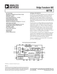
aFEATURES<strong>ADM660</strong>: Inverts or Doubles Input Supply <strong>Voltage</strong><strong>ADM8660</strong>: Inverts Input Supply <strong>Voltage</strong>100 mA Output CurrentShutdown Function (<strong>ADM8660</strong>)2.2 F or 10 F <strong>Capacitor</strong>s0.3 V Drop at 30 mA Load+1.5 V to +7 V SupplyLow Power <strong>CMOS</strong>: 600 A Quiescent CurrentSelectable Charge Pump Frequency (25 kHz/120 kHz)Pin Compatible Upgrade for MAX660, MAX665, ICL7660Available in 16-Lead TSSOP PackageAPPLICATIONSHandheld InstrumentsPortable ComputersRemote Data AcquisitionOp Amp Power SuppliesGENERAL DESCRIPTIONThe <strong>ADM660</strong>/<strong>ADM8660</strong> is a charge-pump voltage converterthat can be used to either invert the input supply voltage givingV OUT = –V IN or double it (<strong>ADM660</strong> only) giving V OUT = 2 × V IN .Input voltages ranging from +1.5 V to +7 V can be inverted intoa negative –1.5 V to –7 V output supply. This inverting schemeis ideal for generating a negative rail in single power supplysystems. Only two small external capacitors are needed for thecharge pump. Output currents up to 50 mA with greater than90% efficiency are achievable, while 100 mA achieves greaterthan 80% efficiency.A Frequency Control (FC) input pin is used to select either25 kHz or 120 kHz charge-pump operation. This is used tooptimize capacitor size and quiescent current. With 25 kHzselected, a 10 µF external capacitor is suitable, while with120 kHz the capacitor may be reduced to 2.2 µF. The oscillatorfrequency on the <strong>ADM660</strong> can also be controlled with an externalcapacitor connected to the OSC input or by driving this inputwith an external clock. In applications where a higher supplyvoltage is desired it is possible to use the <strong>ADM660</strong> to doublethe input voltage. With input voltages from 2.5 V to 7 V, outputvoltages from 5 V to 14 V are achievable with up to 100 mAoutput current.The <strong>ADM8660</strong> features a low power shutdown (SD) pin insteadof the external oscillator (OSC) pin. This can be used todisable the device and reduce the quiescent current to 300 nA.C110µF<strong>CMOS</strong> <strong>Switched</strong>-<strong>Capacitor</strong><strong>Voltage</strong> Converters<strong>ADM660</strong>/<strong>ADM8660</strong>TYPICAL CIRCUIT CONFIGURATIONSFCCAP+GNDCAP–<strong>ADM660</strong>+1.5V TO +7VINPUTC210µFThe <strong>ADM660</strong> is a pin compatible upgrade for the MAX660,MAX665, ICL7660 and LTC1046.The <strong>ADM660</strong>/<strong>ADM8660</strong> is available in 8-pin DIP and narrowbodySOIC. The <strong>ADM660</strong> is also available in a 16-lead TSSOPpackage.<strong>ADM660</strong>/<strong>ADM8660</strong> OptionsOption <strong>ADM660</strong> <strong>ADM8660</strong>Inverting Mode Y YDoubling Mode Y NExternal Oscillator Y NShutdown N YPackage OptionsSO-8 Y YN-8 Y YRU-16 Y NV+OSCLVOUTINVERTEDNEGATIVEOUTPUT<strong>Voltage</strong> Inverter Configuration (<strong>ADM660</strong>)C110µFSHUTDOWNCONTROLFC<strong>ADM8660</strong>CAP+GNDCAP–SDV+LVOUT+1.5V TO +7VINPUTC210µFINVERTEDNEGATIVEOUTPUT<strong>Voltage</strong> Inverter Configuration with Shutdown (<strong>ADM8660</strong>)REV. AInformation furnished by Analog Devices is believed to be accurate andreliable. However, no responsibility is assumed by Analog Devices for itsuse, nor for any infringements of patents or other rights of third partieswhich may result from its use. No license is granted by implication orotherwise under any patent or patent rights of Analog Devices.One Technology Way, P.O. Box 9106, Norwood, MA 02062-9106, U.S.A.Tel: 617/329-4700 World Wide Web Site: http://www.analog.comFax: 617/326-8703 © Analog Devices, Inc., 1997
<strong>ADM660</strong>/<strong>ADM8660</strong>–SPECIFICATIONSParameter Min Typ Max Units Test Conditions/CommentsInput <strong>Voltage</strong>, V+Supply CurrentR L = 1 kΩ3.5 7.0 V Inverting Mode, LV = Open1.5 7.0 V Inverting Mode, LV = GND2.5 7.0 V Doubling Mode, LV = OUTNo Load0.6 1 mA FC = Open (<strong>ADM660</strong>), GND (<strong>ADM8660</strong>)2.5 4.5 mA FC = V+, LV = OpenOutput Current 100 mAOutput Resistance 9 15 Ω I L = 100 mACharge-Pump Frequency 25 kHz FC = Open (<strong>ADM660</strong>), GND (<strong>ADM8660</strong>)120 kHz FC = V+OSC Input Current ±5 µA FC = Open (<strong>ADM660</strong>), GND (<strong>ADM8660</strong>)±25 µA FC = V+Power Efficiency (FC = Open) 90 94 % R L = 1 kΩ Connected from V+ to OUT90 93 % R L = 500 Ω Connected from OUT to GND81.5 % I L = 100 mA to GND<strong>Voltage</strong> Conversion Efficiency 99 99.96 % No LoadShutdown Supply Current, I SHDN 0.3 5 µA <strong>ADM8660</strong>, SHDN = V+Shutdown Input <strong>Voltage</strong>, V SHDN 2.4 V SHDN High = Disabled0.8 V SHDN Low = EnabledShutdown Exit Time 500 µs I L = 100 mANOTES1 C1 and C2 are low ESR (2000 V*This is a stress rating only; functional operation of the device at these or any otherconditions above those indicated in the operation section of this specification is notimplied. Exposure to absolute maximum rating conditions for extended periodsmay affect device reliability.ORDERING GUIDETemperaturePackageModel Range Options*<strong>ADM660</strong>AN –40°C to +85°C N-8<strong>ADM660</strong>AR –40°C to +85°C SO-8<strong>ADM660</strong>ARU –40°C to +85°C RU-16<strong>ADM8660</strong>AN –40°C to +85°C N-8<strong>ADM8660</strong>AR –40°C to +85°C SO-8*N = Plastic DIP; RU = Thin Shrink Small Outline; SO = Small Outline.–2–REV. A
<strong>ADM660</strong>/<strong>ADM8660</strong>PIN FUNCTION DESCRIPTIONSInverter ConfigurationMnemonic FunctionFCFrequency Control Input for Internal Oscillatorand Charge Pump. With FC = Open (<strong>ADM660</strong>)or connected to GND (<strong>ADM8660</strong>), f CP = 25 kHz;with FC = V+, f CP = 120 kHzCAP+ Positive Charge-Pump <strong>Capacitor</strong> Terminal.GND Power Supply Ground.CAP– Negative Charge-Pump <strong>Capacitor</strong> Terminal.OUT Output, Negative <strong>Voltage</strong>.LVLow <strong>Voltage</strong> Operation Input. Connect to GNDwhen input voltage is less than 3.5 V. Above3.5 V, LV may be connected to GND or leftunconnected.OSC <strong>ADM660</strong>: Oscillator Control Input. OSC isconnected to an internal 15 pF capacitor. Anexternal capacitor may be connected to slow theoscillator. An external oscillator may also beused to overdrive OSC. The charge-pumpfrequency is equal to 1/2 the oscillator frequency.SD<strong>ADM8660</strong>: Shutdown Control Input. This input,when high, is used to disable the chargepump thereby reducing the power consumption.V+ Positive Power Supply Input.Doubler Configuration (<strong>ADM660</strong> Only)Mnemonic FunctionFCFrequency Control Input for Internal Oscillatorand Charge Pump. With FC = Open, f CP =25 kHz; with FC = V+, f CP = 120 kHz.CAP+ Positive Charge-Pump <strong>Capacitor</strong> Terminal.GND Positive Input Supply.CAP– Negative Charge-Pump <strong>Capacitor</strong> Terminal.OUT Ground.LVLow <strong>Voltage</strong> Operation Input. Connect to OUT.OSC Must be left unconnected in this mode.V+ Doubled Positive Output.PIN CONNECTIONS8-LeadFCCAP+GND123<strong>ADM660</strong>TOP VIEW(Not to Scale)876V+OSCLVFCCAP+GND123<strong>ADM8660</strong>TOP VIEW(Not to Scale)876V+SDLVCAP–45OUTCAP–45OUT16-LeadNCNCFCCAP+GNDCAP–NCNC12345678<strong>ADM660</strong>RU-16TOP VIEW(Not to Scale)16 NC15 NC14 V+13 OSC12 LV11 OUT10 NC9 NCNC = NO CONNECTREV. A –3–
<strong>ADM660</strong>/<strong>ADM8660</strong>–Typical Performance Characteristics3100IL = 10mASUPPLY CURRENT – mA2.521.51VOLTAGE DOUBLERLV = OUTLV = GNDPOWER EFFICIENCY – %9080706050IL = 1mAIL = 50mA0.5LV = OPEN40IL = 80mA01.5 3.5 5.57.5SUPPLY VOLTAGE – Volts301k 10k100k1MCHARGE-PUMP FREQUENCY – HzFigure 1. Power Supply Current vs. <strong>Voltage</strong>Figure 4. Efficiency vs. Charge-Pump Frequency–31003.5OUTPUT VOLTAGE – VoltsEFFICIENCY–3.4–3.8–4.2V OUT–4.6–500 20 40 60 80 100LOAD CURRENT – mA80604020EFFICIENCY – %SUPPLY CURRENT – mA32.521.510.5LV = GNDVOLTAGE DOUBLERLV = GNDVOLTAGE INVERTER01 101001000CHARGE-PUMP FREQUENCY – kHzFigure 2. Output <strong>Voltage</strong> and Efficiency vs. Load CurrentFigure 5. Power Supply Current vs. Charge-PumpFrequency1.6120OUTPUT VOLTAGE DROPFROM SUPPLY VOLTAGE – Volts1.20.80.4V+ = +1.5VV+ = +2.5VV+ = +3.5VV+ = +5.5VV+ = +4.5VEFFICIENCY – %100806040V+ = +6.5VV+ = +5.5V V+ = +4.5VV+ = +3.5VV+ = +1.5V V+ = +2.5V2000 20 40 60 80 100LOAD CURRENT – mA00 20 40 60 80 100LOAD CURRENT – mAFigure 3. Output <strong>Voltage</strong> Drop vs. Load CurrentFigure 6. Power Efficiency vs. Load Current–4–REV. A
<strong>ADM660</strong>/<strong>ADM8660</strong>535OUTPUT VOLTAGE – Volts4.543.532.521.510.5LOAD = 10mALOAD = 1mALOAD = 50mALOAD = 80mACHARGE-PUMP FREQUENCY – kHz30252015105LV = GNDFC = OPENC1, C2 = 10µF01 10 1001000CHARGE-PUMP FREQUENCY – kHz0–40 –20 0 20 40 60 80TEMPERATURE – °CFigure 7. Output <strong>Voltage</strong> vs. Charge-Pump FrequencyFigure 10. Charge-Pump Frequency vs. Temperature301kOUTPUT SOURCE RESISTANCE – Ω252015105CHARGE-PUMP FREQUENCY – kHz100101FC = OPENLV = GNDFC = V+LV = GND01.5 2.5 3.5 4.5 5.5 6.5SUPPLY VOLTAGE – Volts0.11 10 1001kCAPACITANCE – pFFigure 8. Output Source Resistance vs. Supply <strong>Voltage</strong>Figure 11. Charge-Pump Frequency vs. ExternalCapacitance30140CHARGE-PUMP FREQUENCY – kHz2010LV = GNDLV = OPENFC = OPENOSC = OPENC1, C2 = 10µFCHARGE-PUMP FREQUENCY – kHz12010080604020LV = OPENLV = GNDFC = V+OSC = OPENC1, C2 = 2.2µF01.5 2.5 3.5 4.5 5.5 6.5SUPPLY VOLTAGE – Volts03 3.5 4 4.5 5 5.5 6 6.5 7SUPPLY VOLTAGE – VoltsFigure 9. Charge-Pump Frequency vs. Supply <strong>Voltage</strong>Figure 12. Charge-Pump Frequency vs. Supply <strong>Voltage</strong>REV. A –5–
<strong>ADM660</strong>/<strong>ADM8660</strong>Inverting Negative <strong>Voltage</strong> GeneratorFigures 19 and 20 show the <strong>ADM660</strong>/<strong>ADM8660</strong> configured togenerate a negative output voltage. Input supply voltages from1.5 V up to 7 V are allowable. For supply voltage less than 3 V,LV must be connected to GND. This bypasses the internalregulator circuitry and gives best performance in low voltageapplications. With supply voltages greater than 3 V, LV maybe either connected to GND or left open. Leaving it open facilitatesdirect substitution for the ICL7660.C110µFFCCAP+GNDCAP–<strong>ADM660</strong>V+OSCLVOUT+1.5V TO +7VINPUTC210µFINVERTEDNEGATIVEOUTPUTTable II. <strong>ADM8660</strong> Charge-Pump Frequency SelectionFC OSC Charge Pump C1, C2GND Open 25 kHz 10 µFV+ Open 120 kHz 2.2 µFGND or V+ Ext Cap See Typical CharacteristicsGND Ext CLK Ext CLK Frequency/2C1FCCAP+GNDCAP–<strong>ADM660</strong><strong>ADM8660</strong>V+OSCLVOUT+1.5V TO +7VINPUTC2<strong>CMOS</strong> GATECLK OSCINVERTEDNEGATIVEOUTPUTFigure 19. <strong>ADM660</strong> <strong>Voltage</strong> Inverter ConfigurationC110µFSHUTDOWNCONTROLFC<strong>ADM8660</strong>CAP+GNDCAP–SDV+OUT+1.5V TO +7VINPUTC210µFINVERTEDNEGATIVEOUTPUTFigure 20. <strong>ADM8660</strong> <strong>Voltage</strong> Inverter ConfigurationOSCILLATOR FREQUENCYThe internal charge-pump frequency may be selected to beeither 25 kHz or 120 kHz using the Frequency Control (FC)input. With FC unconnected (<strong>ADM660</strong>) or connected to GND(<strong>ADM8660</strong>), the internal charge pump runs at 25 kHz while, ifFC is connected to V+, the frequency is increased by a factor offive. Increasing the frequency allows smaller capacitors to beused for equivalent performance or, if the capacitor size is unchanged,it results in lower output impedance and ripple.If a charge-pump frequency other than the two fixed values isdesired, this is made possible by the OSC input, which can eitherhave a capacitor connected to it or be overdriven by anexternal clock. Please refer to the Typical Performance Characteristics,which shows the variation in charge-pump frequencyversus capacitor size. The charge-pump frequency is one-halfthe oscillator frequency applied to the OSC pin.If an external clock is used to overdrive the oscillator, its levelsshould swing to within 100 mV of V+ and GND. A <strong>CMOS</strong>driver is, therefore, suitable. When OSC is overdriven, FC hasno effect but LV must be grounded.Note that overdriving is permitted only in the voltageinverter configuration.Table I. <strong>ADM660</strong> Charge-Pump Frequency SelectionFC OSC Charge Pump C1, C2Open Open 25 kHz 10 µFV+ Open 120 kHz 2.2 µFOpen or V+ Ext Cap See Typical CharacteristicsOpen Ext CLK Ext CLK Frequency/2LVFigure 21. <strong>ADM660</strong>/<strong>ADM8660</strong> External Oscillator<strong>Voltage</strong> Doubling ConfigurationFigure 22 shows the <strong>ADM660</strong> configured to generate increasedoutput voltages. As in the inverting mode, only two external capacitorsare required. The doubling function is achieved by reversingsome connections to the device. The input voltage isapplied to the GND pin and V+ is used as the output. Inputvoltages from 2.5 V to 7 V are allowable. In this configuration,pins LV, OUT must be connected to GND.The unloaded output voltage in this configuration is 2 (V IN ).Output resistance and ripple are similar to the voltage invertingconfiguration.Note that the <strong>ADM8660</strong> cannot be used in the voltagedoubling configuration.+2.5VTO +7VINPUT10µFFCCAP+GNDCAP–<strong>ADM660</strong>V+OSCLVOUT10µFFigure 22. <strong>Voltage</strong> Doubler ConfigurationDOUBLEDPOSITIVEOUTPUTShutdown InputThe <strong>ADM8660</strong> contains a shutdown input that can be used todisable the device and hence reduce the power consumption. Alogic high level on the SD input shuts the device down reducingthe quiescent current to 0.3 µA. During shutdown the outputvoltage goes to 0 V. Therefore, ground referenced loads arenot powered during this state. When exiting shutdown it takesseveral cycles (approximately 500 µs) for the charge pump toreach its final value. If the shutdown function is not being used,then SD should be hardwired to GND.<strong>Capacitor</strong> SelectionThe optimum capacitor value selection depends the chargepumpfrequency. With 25 kHz selected, 10 µF capacitors arerecommended, while with 120 kHz selected, 2.2 µF capacitorsmay be used. Other frequencies allow other capacitor values tobe used. For maximum efficiency in all cases, it is recommendedthat capacitors with low ESR are used for the charge pump.Low ESR capacitors give both the lowest output resistance andlowest ripple voltage. High output resistance degrades the overallpower efficiency and causes voltage drops, especially at highREV. A –7–
<strong>ADM660</strong>/<strong>ADM8660</strong>output current levels. The <strong>ADM660</strong>/<strong>ADM8660</strong> is tested usinglow ESR, 10 µF, capacitors for both C1 and C2. Smaller valuesof C1 increase the output resistance, while increasing C1 will reducethe output resistance. The output resistance is also dependenton the internal switches on resistance as well as thecapacitors ESR so the effect of increasing C1 becomes negligiblepast a certain point.Figure 23 shows how the output resistance varies with oscillatorfrequency for three different capacitor values. At low oscillatorfrequencies, the output impedance is dominated by the 1/f Cterm. This explains why the output impedance is higher forsmaller capacitance values. At high oscillator frequencies, the1/f C term becomes insignificant and the output impedance isdominated by the internal switches on resistance. From an outputimpedance viewpoint, therefore, there is no benefit to begained from using excessively large capacitors.OUTPUT RESISTANCE – Ω500400300200100C1 = C2 = 2.2µFC1 = C2 = 10µFC1 = C2 = 1µF00.1 1 10100OSCILLATOR FREQUENCY – kHzBypass <strong>Capacitor</strong>The ac impedance of the <strong>ADM660</strong>/<strong>ADM8660</strong> may be reducedby using a bypass capacitor on the input supply. This capacitorshould be connected between the input supply and GND. Itwill provide instantaneous current surges as required. Suitablecapacitors of 0.1 µF or greater may be used.OUTLINE DIMENSIONSDimensions shown in inches and (mm).80.022 (0.558)0.014 (0.356)0.430 (10.92)0.348 (8.84)1 48-Lead Plastic DIP(N-8)50.280 (7.11)0.240 (6.10)PIN 1 0.060 (1.52)0.015 (0.38)0.210 (5.33)MAX 0.1300.160 (4.06)0.115 (2.93)0.070 (1.77)0.100(2.54) 0.045 (1.15)BSC(3.30)MINSEATINGPLANE0.325 (8.25)0.300 (7.62)8-Lead Narrow-Body SOIC(SO-8)0.1968 (5.00)0.1890 (4.80)0.015 (0.381)0.008 (0.204)0.195 (4.95)0.115 (2.93)C2053a–5–5/97Figure 23. Output Impedance vs. Oscillator Frequency<strong>Capacitor</strong> C2The output capacitor size C2 affects the output ripple. Increasingthe capacitor size reduces the peak-peak ripple. The ESRaffects both the output impedance and the output ripple.Reducing the ESR reduces the output impedance and ripple.For convenience it is recommended that both C1 and C2 be thesame value.Table III. <strong>Capacitor</strong> Selection0.1574 (4.00)0.1497 (3.80)PIN 10.0098 (0.25)0.0040 (0.10)SEATINGPLANE8 51 40.2440 (6.20)0.2284 (5.80)0.0688 (1.75)0.0532 (1.35)0.0500 0.0192 (0.49)(1.27) 0.0138 (0.35)BSC0.0098 (0.25)0.0075 (0.19)8°0°0.0196 (0.50)0.0099 (0.25) x 45°0.0500 (1.27)0.0160 (0.41)Charge-PumpFrequency<strong>Capacitor</strong>C1, C216-Lead TSSOP(RU-16)25 kHz 10 µF120 kHz 2.2 µFPower Efficiency and Oscillator Frequency TradeoffWhile higher switching frequencies allow smaller capacitors tobe used for equivalent performance, or improved performancewith the same capacitors, there is a tradeoff to be considered. Asthe oscillator frequency is increased, the quiescent current increases.This happens as a result of a finite charge being lost ateach switching cycle. The charge loss per unit cycle at very highfrequencies can be significant, thereby reducing the power efficiency.Since the power efficiency is also degraded at low oscillatorfrequencies, due to an increase in output impedance, thismeans that there is an optimum frequency band for maximumpower transfer. Please refer to the Typical Performance Characteristicssection.0.177 (4.50)0.169 (4.30)0.006 (0.15)0.002 (0.05)SEATINGPLANE16 910.201 (5.10)0.193 (4.90)PIN 10.0256(0.65)BSC80.0118 (0.30)0.0075 (0.19)0.256 (6.50)0.246 (6.25)0.0433(1.10)MAX0.0079 (0.20)0.0035 (0.090)8°0°0.028 (0.70)0.020 (0.50)PRINTED IN U.S.A.–8–REV. A