Design and Test of a Scalable Security Processor - ACM Digital ...
Design and Test of a Scalable Security Processor - ACM Digital ...
Design and Test of a Scalable Security Processor - ACM Digital ...

Create successful ePaper yourself
Turn your PDF publications into a flip-book with our unique Google optimized e-Paper software.
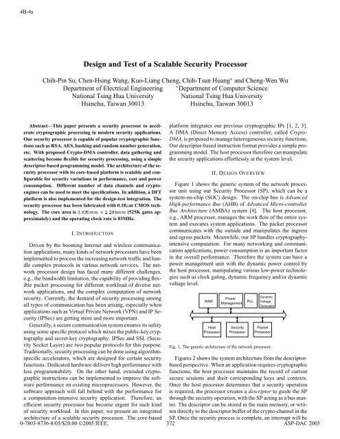
4B-4s<strong>Design</strong> <strong>and</strong> <strong>Test</strong> <strong>of</strong> a <strong>Scalable</strong> <strong>Security</strong> <strong>Processor</strong>Chih-Pin Su, Chen-Hsing Wang, Kuo-Liang Cheng, Chih-Tsun Huang £ <strong>and</strong> Cheng-Wen WuDepartment <strong>of</strong> Electrical Engineering £Department <strong>of</strong> Computer ScienceNational Tsing Hua University National Tsing Hua UniversityHsinchu, Taiwan 30013 Hsinchu, Taiwan 30013Abstract—This paper presents a security processor to acceleratecryptographic processing in modern security applications.Our security processor is capable <strong>of</strong> popular cryptographic functionssuch as RSA, AES, hashing <strong>and</strong> r<strong>and</strong>om number generation,etc. With proposed Crypto-DMA controller, data gathering <strong>and</strong>scattering become flexible for security processing, using a simpledescriptor-based programming model. The architecture <strong>of</strong> the securityprocessor with its core-based platform is scalable <strong>and</strong> configurablefor security variations in performance, cost <strong>and</strong> powerconsumption. Different number <strong>of</strong> data channels <strong>and</strong> cryptoenginescan be used to meet the specifications. In addition, a DFTplatform is also implemented for the design-test integration. Thesecurity processor has been fabricated with 0.18m CMOS technology.The core area is ¿ÑÑ ¢ ¾¾ÑÑ (525K gates approximately)<strong>and</strong> the operating clock rate is 83MHz.I. INTRODUCTIONDriven by the booming Internet <strong>and</strong> wireless communicationapplications, many kinds <strong>of</strong> network processors have beenimplemented to process the increasing network traffic <strong>and</strong> h<strong>and</strong>lecomplex protocols in various network services. The networkprocessor design has faced many different challenges,e.g., the b<strong>and</strong>width limitation, the capability <strong>of</strong> providing flexiblepacket processing for different workload <strong>of</strong> diverse networkapplications, <strong>and</strong> the complex computation <strong>of</strong> networksecurity. Currently, the dem<strong>and</strong> <strong>of</strong> security processing amongall types <strong>of</strong> communication has been arising, especially whenapplications such as Virtual Private Network (VPN) <strong>and</strong> IP <strong>Security</strong>(IPSec) are getting more <strong>and</strong> more important.Generally, a secure communication system ensures its safetyusing some specific protocol which mixes the public-key cryptography<strong>and</strong> secret-key cryptography. IPSec <strong>and</strong> SSL (<strong>Security</strong>Socket Layer) are two popular protocols for this purpose.Traditionally, security processing can be done using algorithmspecificaccelerators, which are designed for certain securityfunctions. Dedicated hardware delivers high performance withless programmability. On the other h<strong>and</strong>, extended cryptographicinstructions can be implemented to improve the s<strong>of</strong>twareperformance on existing microprocessors. However, thes<strong>of</strong>tware approach will fall behind with the performance fora computation-intensive security application. Therefore, anefficient security processor has become urgent for such kind<strong>of</strong> security workload. In this paper, we present an integratedarchitecture <strong>of</strong> a scalable security processor. The core-basedplatform integrates our previous cryptographic IPs [1, 2, 3].A DMA (Direct Memory Access) controller, called Crypto-DMA, is proposed to manage heterogeneous security functions.Our descriptor-based instruction format provides a simple programmingmodel. The host processor therefore can manipulatethe security applications effortlessly at the system level.II. DESIGN OVERVIEWFigure 1 shows the generic system <strong>of</strong> the network processorunit using our <strong>Security</strong> <strong>Processor</strong> (SP), which can be asystem-on-chip (SOC) design. The on-chip bus is AdvancedHigh-performance Bus (AHB) <strong>of</strong> Advanced Micro-controllerBus Architecture (AMBA) system [4]. The host processor,e.g., ARM processor, manages the work flow <strong>of</strong> the entire system<strong>and</strong> executes system applications. The packet processorcommunicates with the outside <strong>and</strong> manipulates the ingress<strong>and</strong> egress packets. Meanwhile, our SP h<strong>and</strong>les cryptographyintensivecomputation. For many networking <strong>and</strong> communicationapplications, power consumption is an important factorin the overall performance. Therefore the system can have apower management unit with the dynamic power control bythe host processor, manipulating various low-power technologiessuch as clock gating, dynamic frequency <strong>and</strong>/or dynamicvoltage level.RAMHost<strong>Processor</strong>PowerManagement<strong>Security</strong><strong>Processor</strong>PLLDynamicVoltageGeneratorPacket<strong>Processor</strong>Fig. 1. The generic architecture <strong>of</strong> the network processor.Figures 2 shows the system architecture from the descriptorbasedperspective. When an application requires cryptographicfunctions, the host processor maintains the record <strong>of</strong> currentsecure sessions <strong>and</strong> their corresponding keys <strong>and</strong> contexts.Once the host processor determines that a security operationis required, the processor creates a descriptor to guide the SPthrough the security operation, with the SP acting as a bus master.The descriptor can be stored in the main memory, or writtendirectly to the descriptor buffer <strong>of</strong> the crypto-channel in theSP. Once the security process is complete, an interrupt will be0-7803-8736-8/05/$20.00 ©2005 IEEE. 372ASP-DAC 2005
asserted to inform the host processor.The descriptor-based scheme reduces the control overhead<strong>of</strong> the host processor. During the cryptographic/authenticationoperations <strong>of</strong> the network applications such as IPSec <strong>and</strong> SSL,the packet/data can be fragmented on the input <strong>and</strong> output.The gathering <strong>and</strong> scattering <strong>of</strong> the encrypted or decrypteddata/packet can be easily achieved by generating the datapointers properly in the descriptor. As a result, our SP, whichinherits the advantages <strong>of</strong> the descriptor-based DMA devices,is capable <strong>of</strong> the data transfer <strong>and</strong> processing workload, leavingthe host processor for the system application <strong>and</strong> the sophisticatedflow control as well as the exception h<strong>and</strong>ling.System MemoryDescriptor #1Descriptor #2Session KeysInput Data #2Input Data #3Input Data #1Output Data #1Output Data #2Output Data #3Descriptor PointerAES ECB Descriptor HeaderPointer <strong>of</strong> KeyLength <strong>of</strong> KeyPointer <strong>of</strong> Input Data #1Length <strong>of</strong> Input Data #1Pointer <strong>of</strong> Output Data #1Length <strong>of</strong> Output Data #1Pointer <strong>of</strong> Input Data #2Length <strong>of</strong> Input Data #2Pointer <strong>of</strong> Output Data #2Length <strong>of</strong> Output Data #2Pointer <strong>of</strong> Input Data #3Length <strong>of</strong> Input Data #3Pointer <strong>of</strong> Output Data #3Length <strong>of</strong> Output Data #3Pointer to Next DescriptorFig. 2. The system architecture <strong>and</strong> data structure <strong>of</strong> a descriptor.III. DESCRIPTOR-BASED INSTRUCTION SETARCHITECTUREAMBA System Bus<strong>Security</strong><strong>Processor</strong>Host<strong>Processor</strong>In Fig. 2, an AES ECB descriptor is shown as a descriptorexample. Figure 3(a) presents the generic descriptor format,which consists <strong>of</strong> 16 32-bit words (64 bytes in total). The firstword is the descriptor header that defines the security operation.Subsequently there are seven pairs <strong>of</strong> data pointer <strong>and</strong>data length. The data pointer refers to the address <strong>of</strong> the datablock, while the data length indicates its amount. Data to betransferred can be interpreted to be keys, initial vector, ciphertext or plain text, etc. The last word <strong>of</strong> the descriptor is anaddress pointer to the next descriptor.The descriptor header defines the cryptographic function<strong>and</strong> its parameters for the security processing. As depictedin Fig. 3(b), the upper halfword <strong>of</strong> the header, the DescriptorControl halfword, identifies the cryptographic function.The most significant three bits (bits 32–29), called the CE(Crypto-Engine) tag, are used to define the category <strong>of</strong> the operations.The CE tag will be used as an identity to reserve thecorresponding crypto-engine. Currently four categories <strong>of</strong> descriptorsare implemented in the prototype, i.e., AES, HMAC,RSA <strong>and</strong> RNG (R<strong>and</strong>om Number Generation). Extension forother cryptographic operations is easy. Two other fields in theDescriptor Control are DH (Descriptor Header)-Type <strong>and</strong> NP(Number <strong>of</strong> Pairs). The DH-Type field further divides the descriptorswith the same CE tag into different types, using bits27 <strong>and</strong> 26. The NP field (bits 18–16) records the total number<strong>of</strong> data blocks referred in the descriptor. The lower halfword<strong>of</strong> the descriptor, the Crypto-Engine Control halfword, definesthe private instruction for the specific crypto-engine. Theinstruction set architecture inherits the original design <strong>of</strong> eachcrypto-engine.In our design, two other AES descriptors, i.e., AES CBC<strong>and</strong> AES Data descriptors are used. Different from the AESECB descriptor (see Fig. 2), the AES CBC descriptor requiresan additional pointer to the initial vector. When the key remainsunchanged, the AES Data descriptor can be used forburst data encryption <strong>and</strong> description. Other descriptor categoriesare defined in a similar way. E.g., the HMAC functionconsists <strong>of</strong> two descriptor types: one is for initialization <strong>of</strong>the HMAC-SHA-1 or HMAC-MD5, <strong>and</strong> the other is for datatransfer. In addition, the RSA descriptor is used to completethe modular exponentiation in the RSA function. The RNGdescriptor is used to retrieve arbitrary length <strong>of</strong> r<strong>and</strong>om number.With descriptor-based data processing, host processor canleave security-intensive computation to the SP with little controloverhead.Descriptor HeaderPointer <strong>of</strong> Data #1Length <strong>of</strong> Data #1Pointer <strong>of</strong> Data #2Length <strong>of</strong> Data #2Pointer <strong>of</strong> Data #3Length <strong>of</strong> Data #3Pointer <strong>of</strong> Data #4Length <strong>of</strong> Data #4Pointer <strong>of</strong> Data #5Length <strong>of</strong> Data #5Pointer <strong>of</strong> Data #6Length <strong>of</strong> Data #6Pointer <strong>of</strong> Data #7Length <strong>of</strong> Data #7Pointer to Next Descriptor(a)Descriptor Control halfwordCryptoEngine Control haflword31 16 0CEAES Descriptor HeaderDH0 0 1 TypeRSA Descriptor Header0 1 1HMAC Descriptor HeaderDH0 1 0 TypeRNG Descriptor Header1 0 0Number<strong>of</strong> PairsE/DModeKeySizeNumber<strong>of</strong> Pairs(b)OpCodeNumber<strong>of</strong> PairsInclude final word addressinclude output addressDESRecompute KeyRunRecompute IVSRC1RunSHA1/MD5Fig. 3. (a) General format <strong>of</strong> a descriptor <strong>and</strong> (b) the definition <strong>of</strong> thedescriptor header.IV. SCALABLE SP ARCHITECTUREThe scalable architecture <strong>of</strong> the proposed SP is shownin Fig. 4. It consists <strong>of</strong> heterogeneous crypto-engines <strong>and</strong>a DMA-like interface, called Crypto-DMA controller. TheCrypto-DMA controller interprets the descriptors <strong>and</strong> manipulatesthe crypto-engines to perform proper cryptographic operations.Direct access <strong>of</strong> specific crypto-engine is also allowedfrom the external AHB interface. Multiple crypto-engines <strong>of</strong>the same <strong>and</strong>/or different cryptographic functions can be used,all with AHB slave interface. Therefore, efforts <strong>of</strong> the integration<strong>and</strong> extension can be minimized. <strong>Design</strong> parameters inthe SP, such as the number <strong>of</strong> crypto-channels, the number <strong>of</strong>crypto-engines, <strong>and</strong> the number <strong>of</strong> internal AHB bus (multilayerAHB), are all scalable <strong>and</strong> configurable to meet differentperformance/area trade-<strong>of</strong>fs. In this paper, the prototypeto realize the architecture shown in Fig. 4 is addressed. OneCrypto-DMA with four crypto-channels has been implementedto control six crypto-engines, including two AES engines [1],two HMAC engines [3], one RSA engine [2], <strong>and</strong> one RNGengine. In this prototype, both the external <strong>and</strong> internal AHBinterfaces are 32 bits.373SRC2
External AHBExternalAHB SlaveInterfaceExternalAHB MasterwithTransferEngineDescriptorBuffer16x32 bitCryptoDMACrypto−Channel #0<strong>Security</strong> <strong>Processor</strong>Input/OutputData FIFO16x32 bitRegister Files 3x32 bitCrypto−Channel #1Crypto−Channel #2Crypto−Channel #3Main ControllerInstructionDecoderResourceManagerMicroprogramSequencerInternalAHB MasterwithTransferEngineFig. 4. <strong>Scalable</strong> architecture <strong>of</strong> <strong>Security</strong> <strong>Processor</strong>.A. Crypto-DMAInternal AHBCryptoEnginesAES#1AES#2HMAC#1HMAC#2RSA#1RNG#1The Crypto-DMA serves as a bridge between the externalsystem memory <strong>and</strong> the internal crypto-engines for thedata transfer. The control flow <strong>of</strong> the internal crypto-enginesis also managed by the Crypto-DMA. Similar to the typicaldescriptor-based DMA devices, the Crypto-DMA is activatedby writing a descriptor pointer to one <strong>of</strong> the Crypto-Channel.The Crypto-DMA will fetch the descriptor <strong>and</strong> interpret thecontent based on the descriptor header. The basic proceduresto process a descriptor are: 1) Assigning specific crypto-engineaccording to the the CE tag in the descriptor header. Whenthere are multiple crypto-engines <strong>of</strong> the same function, theirstatus <strong>and</strong> priority will also be considered. 2) Initializing thetargeted crypto-engine. 3) Transferring the data from the systemmemory to the input buffer or local memory <strong>of</strong> the targetedcrypto-engine. 4) Activating the cryptographic processing. 5)Transferring the data from the output buffer or local memory<strong>of</strong> the targeted crypto-engine back to the external memory afterreceiving the interrupt <strong>of</strong> the completeness from the cryptoengine.6) Releasing the targeted crypto-engine. 7) Automaticallyfetching the successive descriptors from the system memory.Although the programming sequences are diverse in differentcrypto-engines, all <strong>of</strong> them can be partitioned into threekinds <strong>of</strong> subsequences: 1) the data input/output state thattransfers the data into or out <strong>of</strong> the crypto-engine; 2) the controlstate that configures the operation mode <strong>of</strong> the crypto-engine<strong>and</strong> 3) the wait state that waits for the data processing <strong>of</strong> thecrypto-engine. Proper interleaving among the sequences <strong>of</strong>different crypto-channels is realized by the Main Controllerin our Crypto-DMA. The interrupt mechanism between theCrypto-DMA <strong>and</strong> crypto-engines is also used to provide thebetter flow control.B. Crypto-EnginesAES Engine—The AES engine is implemented based on thework in [1]. It supports the st<strong>and</strong>ard AES encryption <strong>and</strong> decryptionwith 128-, 192- <strong>and</strong> 256-bit keys, with both ECB <strong>and</strong>CBC modes. In addition to the previous approach using a costeffectivecomposite field arithmetic, this improvement reducesthe critical path by moving the basis conversion hardware between ´¾ µ <strong>and</strong> ´´¾ µ ¾ µ outside the round iteration.RSA Engine—The RSA engine [2] performs the modularmultiplication based on an enhanced word-based Montgomeryalgorithm, supporting scalable keys <strong>of</strong> the length up to 1024bits.HMAC Engine—The HMAC engine is based on the work in[3], which proposed an area-efficient integrated SHA-1/MD5core.RNG Engine—The RNG engine is a pseudo r<strong>and</strong>om numbergenerator that consists <strong>of</strong> five linear feed-back shift registers(LFSRs) with different structures <strong>and</strong> data scrambling in theoutput. The fully-synthesizable implementation makes it easyto integrate into the SP. Our RNG also provides a single-bitnoise input. By introducing the 1-bit noise source into theRNG, the output will become unpredictable. Our RNG hasbeen validated by the r<strong>and</strong>om number test in the FIPS 140-2st<strong>and</strong>ard [5].V. DFT PLATFORMFollowing the core-based design methodology, the SP ispartitioned into the Crypto-DMA <strong>and</strong> crypto-engine cores.Each crypto-engine has been designed <strong>and</strong> verified individually.Therefore, the major verification effort focuses on theCrypto-DMA <strong>and</strong> the interconnection. In the design flow, thetest planning is taken into account from the beginning. Figure 5shows our design <strong>and</strong> test integration flow to realize the SP design.Here we utilize STEAC (SOC TEst Aid Console) [6]framework to help the test integration. All the crypto-enginescome as the synthesized scan-ready netlist. The DFT information<strong>of</strong> crypto-engines generated by the commercial ATPGare submitted to the STEAC to generate the first pass <strong>of</strong> testscheduling. The first-pass test scheduling provides a referenceresult <strong>of</strong> the overall test time with respect to the width <strong>of</strong> TAM(<strong>Test</strong> Access Mechanism) bus <strong>and</strong> the number <strong>of</strong> scan chainsfor each IP. The test access architecture can be further adjustedbased on this reference, resulting in an optimized test scheduling<strong>and</strong> test access architecture in the second pass. Based onthis result, the TAM circuitry, test controller as well as the testwrappers are generated accordingly. These DFT circuits arethen integrated into the SP with the typical synthesis flow. Thetest patterns <strong>of</strong> each core can also be translated to system levelby the STEAC easily. The overall test architecture <strong>of</strong> the SP isshowninFig.6. VI. IMPLEMENTATION RESULTSOur chip has been fabricated using UMC 0.18m CMOSst<strong>and</strong>ard library. Table I summarizes the area statistics <strong>of</strong> theSP. <strong>Test</strong> circuitry occupies less then 1% <strong>of</strong> the total gate countwith negligible performance penalty. Our DFT wrappers areresided in the bus interface, avoiding the extra timing overheadto the critical path.A layout view <strong>of</strong> the whole chip<strong>and</strong> its floorplaning is depicted in Fig. 7. Total chip area isÑÑ ¢ ¿½ÑÑ, where the core area is ¿ÑÑ ¢¾¾ÑÑ. The equivalent gate count is about 525K gates. Theoperating frequency is about 83MHz under post-layout simulation.Total power consumption is about 383.5mW.Table II shows the peak performance considering the maximumoperating frequency <strong>of</strong> the individual crypto-engine. In374