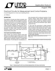
1 Megabit (128K x 8) 5-volt Only CMOS Flash Memory AT29C010A
1 Megabit (128K x 8) 5-volt Only CMOS Flash Memory AT29C010A
1 Megabit (128K x 8) 5-volt Only CMOS Flash Memory AT29C010A
- No tags were found...

Create successful ePaper yourself
Turn your PDF publications into a flip-book with our unique Google optimized e-Paper software.
<strong>AT29C010A</strong>FeaturesFast Read Access Time - 70 ns5-Volt-<strong>Only</strong> Reprogramming• Sector Program OperationSingle Cycle Reprogram (Erase and Program)1024 Sectors (128 bytes/sector)Internal Address and Data Latches for 128-BytesTwo 8 KB Boot Blocks with LockoutInternal Program Control and TimerHardware and Software Data ProtectionFast Sector Program Cycle Time - 10 msDATA Polling for End of Program Detection• Low Power Dissipation50 mA Active Current100 µA <strong>CMOS</strong> Standby Current• Typical Endurance > 10,000 CyclesSingle 5V ±10% Supply<strong>CMOS</strong> and TTL Compatible Inputs and Outputs• Commercial and Industrial Temperature RangesDescriptionThe <strong>AT29C010A</strong> is a 5-<strong>volt</strong>-only in-system <strong>Flash</strong> programmable and erasable readonly memory (PEROM). Its 1 megabit of memory is organized as 131,072 words by 8bits. Manufactured with Atmel’s advanced nonvolatile <strong>CMOS</strong> technology, the deviceoffers access times to 70 ns with power dissipation of just 275 mW over the commercialtemperature range. When the device is deselected, the <strong>CMOS</strong> standby current isless than 100 µA. The device endurance is such that any sector can typically be writtento in excess of 10,000 times.To allow for simple in-system reprogrammability, the <strong>AT29C010A</strong> does not requirehigh input <strong>volt</strong>ages for programming. Five-<strong>volt</strong>-only commands determine the opera-Pin ConfigurationsPin NameA0 - A16CEOEWEI/O0 - I/O7NCFunctionAddressesChip EnableOutput EnableWrite EnableData Inputs/OutputsNo ConnectDIP Top View(continued)1 <strong>Megabit</strong>(<strong>128K</strong> x 8)5-<strong>volt</strong> <strong>Only</strong><strong>CMOS</strong> <strong>Flash</strong><strong>Memory</strong><strong>AT29C010A</strong>PLCC Top ViewTSOP Top ViewType 10394B4-129
Device Operation (Continued)BOOT BLOCK LOCKOUT DETECTION: A softwaremethod is available to determine whether programming ofeither boot block section is locked out. See Software ProductIdentification Entry and Exit sections. When the deviceis in the software product identification mode, a read fromlocation 00002 will show if programming the lower addressboot block is locked out while reading location FFFF2 willDC and AC Operating RangeOperating ModesMode CE OE WE Ai I/ORead VIL VIL VIH Ai DOUTProgram (2) VIL VIH VIL Ai DIN5V Chip Erase VIL VIH VIL AiStandby/Write Inhibit VIH X (1) X X High ZProgram Inhibit X X VIHProgram Inhibit X VIL XOutput Disable X VIH X High ZProduct IdentificationHardware VIL VIL VIHA1 - A16 = V IL, A9 = V H, (3)A0 = V ILManufacturer Code (4)A1 - A16 = V IL, A9 = V H, (3)A0 = V IHDevice Code (4)Software (5) A0 = V IL Manufacturer Code (4)A0 = V IH Device Code (4)Notes: 1. X can be V IL or V IH.2. Refer to AC Programming Waveforms.3. V H = 12.0V ± 0.5V.DC Characteristicsdo so for the upper boot block. If the data is FE, the correspondingblock can be programmed; if the data is FF, theprogram lockout feature has been activated and the correspondingblock cannot be programmed. The softwareproduct identification exit mode should be used to return tostandard operation.<strong>AT29C010A</strong>-70 <strong>AT29C010A</strong>-90 <strong>AT29C010A</strong>-12 <strong>AT29C010A</strong>-15OperatingCom. 0°C - 70°C 0°C - 70°C 0°C - 70°C 0°C - 70°CTemperature (Case) Ind. -40°C - 85°C -40°C - 85°C -40°C - 85°CVCC Power Supply 5V ± 5% 5V ± 10% 5V ± 10% 5V ± 10%4. Manufacturer Code: 1F, Device Code: D55. See details under Software Product Identification Entry/Exit.Symbol Parameter Condition Min Max UnitsILI Input Load Current VIN = 0V to VCC 10 µAILO Output Leakage Current VI/O = 0V to VCC 10 µAISB1 VCC Standby Current <strong>CMOS</strong> CE = VCC - 0.3V to VCCCom. 100 µAInd. 300 µAISB2 VCC Standby Current TTL CE = 2.0V to VCC 3 mAICC VCC Active Current f = 5 MHz; IOUT = 0 mA 50 mAVIL Input Low Voltage 0.8 VVIH Input High Voltage 2.0 VVOL Output Low Voltage IOL = 2.1 mA .45 VVOH1 Output High Voltage IOH = -400 µA 2.4 VVOH2 Output High Voltage <strong>CMOS</strong> IOH = -100 µA; VCC = 4.5V 4.2 V4-132 <strong>AT29C010A</strong>
AC Byte Load CharacteristicsSymbol Parameter Min Max UnitstAS, tOES Address, OE Set-up Time 0 nstAH Address Hold Time 50 nstCS Chip Select Set-up Time 0 nstCH Chip Select Hold Time 0 nstWP Write Pulse Width (WE or CE) 90 nstDS Data Set-up Time 35 nstDH, tOEH Data, OE Hold Time 0 nstWPH Write Pulse Width High 100 nsAC Byte Load WaveformsWE ControlledCE Controlled4-134 <strong>AT29C010A</strong>
<strong>AT29C010A</strong>Program Cycle CharacteristicsSymbol Parameter Min Max UnitstWC Write Cycle Time 10 mstAS Address Set-up Time 0 nstAH Address Hold Time 50 nstDS Data Set-up Time 35 nstDH Data Hold Time 0 nstWP Write Pulse Width 90 nstBLC Byte Load Cycle Time 150 µstWPH Write Pulse Width High 100 ns(1, 2, 3)Program Cycle WaveformsNotes: 1. A7 through A16 must specify the sector addressduring each high to low transition of WE (or CE).2. OE must be high when WE and CE are both low.3. All bytes that are not loaded within the sector beingprogrammed will be indeterminate.4-135
Software DataProtection Enable Algorithm (1)LOAD DATA AATOADDRESS 5555LOAD DATA 55TOADDRESS 2AAASoftware DataProtection Disable Algorithm (1)LOAD DATA AATOADDRESS 5555LOAD DATA 55TOADDRESS 2AAALOAD DATA A0TOADDRESS 5555LOAD DATATOSECTOR (128 BYTES) (4)WRITES ENABLEDENTER DATAPROTECT STATE (2)Notes for software program code:1. Data Format: I/O7 - I/O0 (Hex);Address Format: A14 - A0 (Hex).2. Data Protect state will be activated at end of program cycle.3. Data Protect state will be deactivated at end ofprogram period.4. 128-bytes of data MUST BE loaded.LOAD DATA 80TOADDRESS 5555LOAD DATA AATOADDRESS 5555LOAD DATA 55TOADDRESS 2AAALOAD DATA 20TOADDRESS 5555LOAD DATATOSECTOR (128 BYTES) (4)EXIT DATAPROTECT STATE (3)(1, 2, 3)Software Protected Program Cycle WaveformNotes: 1. A7 through A16 must specify the sector addressduring each high to low transition of WE (or CE)after the software code has been entered.2. OE must be high when WE and CE are both low.3. All bytes that are not loaded within the sector beingprogrammed will be indeterminate.4-136 <strong>AT29C010A</strong>
<strong>AT29C010A</strong>Data Polling Characteristics (1)Symbol Parameter Min Typ Max UnitstDH Data Hold Time 10 nstOEH OE Hold Time 10 nstOE OE to Output Delay (2) nstWR Write Recovery Time 0 nsNotes: 1. These parameters are characterized and not 100% tested.2. See t OE spec in AC Read Characteristics.Data Polling WaveformsToggle Bit Characteristics (1)Symbol Parameter Min Typ Max UnitstDH Data Hold Time 10 nstOEH OE Hold Time 10 nstOE OE to Output Delay (2) nstOEHP OE High Pulse 150 nstWR Write Recovery Time 0 nsNotes: 1. These parameters are characterized and not 100% tested.2. See t OE spec in AC Read Characteristics.(1, 2, 3)Toggle Bit WaveformsNotes: 1. Toggling either OE or CE or both OE and CE willoperate toggle bit.2. Beginning and ending state of I/O6 will vary.3. Any address location may be used but the addressshould not vary.4-137
Software ProductIdentification Entry (1)LOAD DATA AATOADDRESS 5555LOAD DATA 55TOADDRESS 2AAABoot Block LockoutFeature Enable Algorithm (1)LOAD DATA AATOADDRESS 5555LOAD DATA 55TOADDRESS 2AAALOAD DATA 90LOAD DATA 80TOTOADDRESS 5555ADDRESS 5555LOAD DATA AAPAUSE 10 mSTOENTER PRODUCTADDRESS 5555IDENTIFICATION(2, 3, 5)MODE LOAD DATA 55TOADDRESS 2AAASoftware ProductIdentification Exit (1) LOAD DATA 40TOADDRESS 5555LOAD DATA AATOADDRESS 5555LOAD DATA 00LOAD DATA FFLOAD DATA 55TOTOTOADDRESS 00000 (2) ADDRESS FFFFF (3)ADDRESS 2AAALOAD DATA F0TOADDRESS 5555PAUSE 10 mSPAUSE 10 mSPAUSE 10 mSEXIT PRODUCTIDENTIFICATIONMODE (4)Notes for boot block lockout feature enable:1. Data Format: I/O7 - I/O0 (Hex);Address Format: A14 - A0 (Hex).2. Lockout feature set on lower address boot block.3. Lockout feature set on higher address boot block.Notes for software product identification:1. Data Format: I/O7 - I/O0 (Hex);Address Format: A14 - A0 (Hex).2. A1 - A16 = V IL.Manufacture Code is read for A0 = V IL;Device Code is read for A0 = V IH.3. The device does not remain in identification mode ifpowered down.4. The device returns to standard operation mode.5. Manufacturer Code: 1FDevice Code: D54-138 <strong>AT29C010A</strong>
<strong>AT29C010A</strong>4-139
tACC(ns)ActiveICC (mA)StandbyOrdering Code Package Operation Range70 50 0.1 <strong>AT29C010A</strong>-70JC 32J Commercial<strong>AT29C010A</strong>-70PC 32P6 (0° to 70°C)<strong>AT29C010A</strong>-70TC32T90 50 0.1 <strong>AT29C010A</strong>-90JC 32J Commercial<strong>AT29C010A</strong>-90PC 32P6 (0° to 70°C)<strong>AT29C010A</strong>-90TC32T50 0.3 <strong>AT29C010A</strong>-90JI 32J Industrial<strong>AT29C010A</strong>-90PI 32P6 (-40° to 85°C)<strong>AT29C010A</strong>-90TI32T120 50 0.1 <strong>AT29C010A</strong>-12JC 32J Commercial<strong>AT29C010A</strong>-12PC 32P6 (0° to 70°C)<strong>AT29C010A</strong>-12TC32T50 0.3 <strong>AT29C010A</strong>-12JI 32J Industrial<strong>AT29C010A</strong>-12PI 32P6 (-40° to 85°C)<strong>AT29C010A</strong>-12TI32T150 50 0.1 <strong>AT29C010A</strong>-15JC 32J Commercial<strong>AT29C010A</strong>-15PC 32P6 (0° to 70°C)<strong>AT29C010A</strong>-15TC32T50 0.3 <strong>AT29C010A</strong>-15JI 32J Industrial<strong>AT29C010A</strong>-15PI 32P6 (-40° to 85°C)<strong>AT29C010A</strong>-15TI32TPackage Type32J32P632T32 Lead, Plastic J-Leaded Chip Carrier (PLCC)32 Lead, 0.600" Wide, Plastic Dual Inline Package (PDIP)32 Lead, Thin Small Outline Package (TSOP)4-140 <strong>AT29C010A</strong>