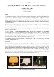
As originally published in the SMTA International Conference Proceedings.Each <strong>of</strong> these metrics can be applied to the <strong>stencil</strong> printingprocess to characterize the relationship between processinputs <strong>and</strong> outputs. In the following study, they are used toselect the best <strong>stencil</strong> options for a high volume, productionoperation.EXPERIMENTAL SETUPTest VehicleTest VehicleFigure 1. Test Vehicle (non-BGA circuitry on closeup isintentionally blurred)The PCB shown in fig 1 is a typical high-volume productionproduct. Each 32-up array measures approximately 3x7inches, <strong>and</strong> has nearly 15,000 SMT pads. Of the 14,468pads, roughly 8500 are mask-defined (SMD) BGA pads <strong>and</strong>1900 are metal-defined (NSMD) 0201 pads. The same set<strong>of</strong> 10 PCBs were used for all tests.Suppliers A & D applied the coating at their sites, prior toshipping the <strong>stencil</strong>s. The same coating product was appliedto <strong>stencil</strong>s provided by <strong>suppliers</strong> B & C after arriving at theVicor facility.Test MatrixFour <strong>suppliers</strong>, coded A-D, submitted <strong>stencil</strong>s in a variety <strong>of</strong>configurations. Materials, coded 1-5, included: Electr<strong>of</strong>ormed <strong>stencil</strong>s (#1) Electr<strong>of</strong>ormed nickel <strong>foil</strong>s that were laser cut (#2) St<strong>and</strong>ard 301SS (#5) 304SS designed for laser cutting (#3) 301SS with modified grain size (#4)Thicknesses <strong>of</strong> the <strong>foil</strong>s included 0.0045” <strong>and</strong> 0.004”. Thecurrent production st<strong>and</strong>ard is 0.0045” laser cut nickel <strong>foil</strong>s.0.004” is under consideration because the preferred 0.0045”is not available in rolled steel.Electropolished <strong>stencil</strong>s were not tested in this <strong>evaluation</strong>,because not all <strong>suppliers</strong> provide electropolishing capability,<strong>and</strong> while electropolised apertures have been reported torelease higher volumes <strong>of</strong> paste due to their roundedcorners, 2 they have also reported to produce higher rates <strong>of</strong>variation in volume consistency. 3For each <strong>stencil</strong>, 10 prints were taken, providing roughly85,000 BGA paste deposit measurements <strong>and</strong> 19,000 0201deposit measurements. The test prints were producedsequentially on a well maintained <strong>and</strong> calibrated 2009 DEKhorizon <strong>stencil</strong> printer using, both front-to-back <strong>and</strong> backto-frontsqueegee strokes, with an automatic dry wipe aftereach print. Print parameters were: Print speed: 15 mm/sec Print pressure: 5 kg (250mm blades) Separation speed: 20mm/secThe solder paste used in all tests was Indium 3.2 HF Type 3,water soluble, lead-free, halogen-free, lot # 37310. Freshpaste was used on each <strong>stencil</strong>. The paste was not kneaded;2 dummy prints were produced before measurements weretaken. The 27 <strong>stencil</strong>s were print tested in a climatecontrolled NPI manufacturing area over 5 different runs.During the tests the climate ranged from 23.0 to 25.5 o C, <strong>and</strong>relative humidity ranged from 32.9 to 46.9%.The PCB was supported with a flat, non-vacuum toolingplate <strong>and</strong> edge clamps. Deposit volume measurements weretaken with a Koh Young 3030VAL.StencilsEach supplier was invited to submit <strong>stencil</strong>s in pairs. One<strong>stencil</strong> was printed in the as-received condition; the otherhad a hydrophobic nanocoating applied before printing.
As originally published in the SMTA International Conference Proceedings.Table 1. Experimental MatrixNo. Supplier Material Nano Coat Thickness1 A 4 N 4.02 B 2 N 4.03 B 2 Y 4.04 C 1 Y 4.55 A 4 Y 4.06 A 3 Y 4.07 A 3 N 4.08 B 1 Y 4.59 B 1 N 4.510 B 1 Y 4.011 B 1 N 4.012 C 2 N 4.513 C 2 Y 4.514 C 1 N 4.515 B 2 Y 4.516 B 2 N 4.517 D 1 Y 4.518 D 2 N 4.519 D 2 Y 4.520 D 3 N 4.021 D 3 Y 4.022 D 4 N 4.023 D 4 Y 4.024 D 5 N 4.025 D 5 Y 4.026 D 1 N 4.527 D 1 N 4.5Not all <strong>suppliers</strong> provided all combinations <strong>of</strong> <strong>materials</strong> <strong>and</strong>thicknesses. The matrix <strong>of</strong> submitted <strong>and</strong> tested <strong>stencil</strong>s isshown in table 1. The single unpaired <strong>stencil</strong>, labelednumber 26, was an experimental run by one <strong>of</strong> the <strong>suppliers</strong>to investigate the effects <strong>of</strong> a process change.RESULTSAperture MeasurementsTable 2. Average Aperture measurementMaterial No. Supplier BGA Dia0201 0201Width Length4 C 10.1 11.0 13.18 B 9.9 11.0 13.09 B 10.0 11.1 13.110 B 10.5 11.6 13.51 11 B 10.4 11.4 13.314 C 10.0 11.0 13.217 D 9.5 10.7 12.726 D 9.5 10.7 12.627 D 9.4 10.6 12.52 B 10.2 11.1 13.13 B 10.2 11.1 13.012 C 9.9 10.9 12.9213 C 9.9 10.9 12.815 B 10.1 11.0 13.016 B 10.1 11.0 12.918 D 10.4 11.3 13.219 D 10.4 11.3 13.36 A 10.5 11.4 13.437 A 10.5 11.4 13.320 D 10.5 11.5 13.421 D 10.5 11.5 13.41 A 10.5 11.5 13.545 A 10.5 11.6 13.522 D 10.5 11.5 13.423 D 10.5 11.5 13.4524 D 10.5 11.4 13.325 D 10.4 11.4 13.3SPEC 10.8 11.8 13.8average 10.2 11.2 13.1