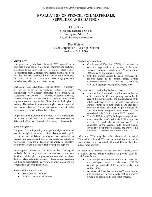
evaluation of stencil foil materials, suppliers and ... - IPC Outlook
evaluation of stencil foil materials, suppliers and ... - IPC Outlook
evaluation of stencil foil materials, suppliers and ... - IPC Outlook

Create successful ePaper yourself
Turn your PDF publications into a flip-book with our unique Google optimized e-Paper software.
As originally published in the SMTA International Conference Proceedings.EVALUATION OF STENCIL FOIL MATERIALS,SUPPLIERS AND COATINGSChrys SheaShea Engineering ServicesBurlington, NJ, USAchrys@sheaengineering.comRay WhittierVicor Corporation – VI Chip DivisionAndover, MA, USAABSTRACTThe past few years have brought PCB assemblers amultitude <strong>of</strong> choices for SMT <strong>stencil</strong> <strong>materials</strong> <strong>and</strong> coatings.In addition to the traditional laser-cut stainless steel (SS) orelectr<strong>of</strong>ormed nickel, choices now include SS that has beenoptimized for laser cutting, SS with smaller grain structures,<strong>and</strong> laser cut nickel. Available post-cutting processesinclude electrpolishing <strong>and</strong> nano-coating.Each option touts advantages over the others. To identifythe best options for the real-world application <strong>of</strong> a highlyminiaturized, very densely populated SMT product, anexperiment was devised. It included different <strong>materials</strong>,manufacturing methods <strong>and</strong> <strong>suppliers</strong>. Stencils were testedin pairs in order to capture the effects <strong>of</strong> a new hydrophobiccoating. The surface treatment was applied to one <strong>stencil</strong> <strong>of</strong>each pair, allowing for direct comparison <strong>of</strong> printperformance with <strong>and</strong> without the coating.Output variables included print yields, transfer efficiencieson 0.5mm BGAs <strong>and</strong> 0201s, volume repeatabilities onBGAs <strong>and</strong> 0201s, <strong>and</strong> dimensional accuracy <strong>of</strong> the <strong>stencil</strong>s.INTRODUCTIONThe goal <strong>of</strong> <strong>stencil</strong> printing is to get the right amount <strong>of</strong>paste in the right location, every time. To support that goal,a number <strong>of</strong> analytical techniques are available tocharacterize, quantify, <strong>and</strong> monitor the inputs <strong>and</strong> outputs <strong>of</strong>the process. They are all based on the ability to accuratelymeasure the volumes <strong>of</strong> individual solder paste deposits.Paste deposit volumes can be measured by a variety <strong>of</strong>methods; the currently available best-in-class method usesstructured white light in a process known as Moire, phaseshift, or white light interferometry. Paste volume readingscan then be manipulated in a variety <strong>of</strong> ways to analyze theprocess from different perspectives.Basic statistics are calculated: Average (mean) volume St<strong>and</strong>ard deviation <strong>of</strong> volumeVariability is examined: Coefficient <strong>of</strong> Variation (CV%), is the st<strong>and</strong>arddeviation expressed as a percent <strong>of</strong> the meanvolume. Generally speaking, a CV <strong>of</strong> less than10% indicates a repeatable process. Cpk, the process capability index, compares theprocess output to its control limits. Typicalbenchmarks include 1.33, 1.67 <strong>and</strong> 2.0, indicating4, 5 <strong>and</strong> 6-sigma process quality, respectively.The paste-<strong>stencil</strong> relationship is characterized: Aperture Area Ratio (AR), is calculated as the area<strong>of</strong> the aperture’s PCB-side opening divided by thearea <strong>of</strong> the aperture walls, <strong>and</strong> is an indicator <strong>of</strong> therelative adhesive forces on the solder paste depositduring separation from the <strong>stencil</strong>. As area ratiosdecrease, so does the amount <strong>of</strong> paste transferred.The minimum acceptable area ratio is <strong>of</strong>tenconsidered to be 0.66 for typical SMT purposes. Transfer Efficiency (TE), is the percentage <strong>of</strong> pastethat is actually transferred to the PCB, as opposedto that left inside the <strong>stencil</strong> aperture. 1 It iscalculated as the average paste deposit volumedivided by the aperture’s volume, <strong>and</strong> expressed asa percent. A common benchmark is 80% TE.ARs <strong>and</strong> TE’s may be either theoretical or actual.Theoretical ARs <strong>and</strong> TEs are calculated from the <strong>stencil</strong>specification, whereas actual ARs <strong>and</strong> TEs are based onactual measurements.In addition to derived indices, production yields, whenavailable, are the ultimate indicator <strong>of</strong> process capability<strong>and</strong> fitness for use. Print test yields are measured at the PCB level, notthe per-deposit level. In the case <strong>of</strong> 10,000deposits per print, all 10,000 must fall within theircontrol limits. An output <strong>of</strong> 1 bad deposit <strong>and</strong> 9,999 good ones ona PCB would not be considered a 100 ppm process;it would be considered a zero yield process.
As originally published in the SMTA International Conference Proceedings.Each <strong>of</strong> these metrics can be applied to the <strong>stencil</strong> printingprocess to characterize the relationship between processinputs <strong>and</strong> outputs. In the following study, they are used toselect the best <strong>stencil</strong> options for a high volume, productionoperation.EXPERIMENTAL SETUPTest VehicleTest VehicleFigure 1. Test Vehicle (non-BGA circuitry on closeup isintentionally blurred)The PCB shown in fig 1 is a typical high-volume productionproduct. Each 32-up array measures approximately 3x7inches, <strong>and</strong> has nearly 15,000 SMT pads. Of the 14,468pads, roughly 8500 are mask-defined (SMD) BGA pads <strong>and</strong>1900 are metal-defined (NSMD) 0201 pads. The same set<strong>of</strong> 10 PCBs were used for all tests.Suppliers A & D applied the coating at their sites, prior toshipping the <strong>stencil</strong>s. The same coating product was appliedto <strong>stencil</strong>s provided by <strong>suppliers</strong> B & C after arriving at theVicor facility.Test MatrixFour <strong>suppliers</strong>, coded A-D, submitted <strong>stencil</strong>s in a variety <strong>of</strong>configurations. Materials, coded 1-5, included: Electr<strong>of</strong>ormed <strong>stencil</strong>s (#1) Electr<strong>of</strong>ormed nickel <strong>foil</strong>s that were laser cut (#2) St<strong>and</strong>ard 301SS (#5) 304SS designed for laser cutting (#3) 301SS with modified grain size (#4)Thicknesses <strong>of</strong> the <strong>foil</strong>s included 0.0045” <strong>and</strong> 0.004”. Thecurrent production st<strong>and</strong>ard is 0.0045” laser cut nickel <strong>foil</strong>s.0.004” is under consideration because the preferred 0.0045”is not available in rolled steel.Electropolished <strong>stencil</strong>s were not tested in this <strong>evaluation</strong>,because not all <strong>suppliers</strong> provide electropolishing capability,<strong>and</strong> while electropolised apertures have been reported torelease higher volumes <strong>of</strong> paste due to their roundedcorners, 2 they have also reported to produce higher rates <strong>of</strong>variation in volume consistency. 3For each <strong>stencil</strong>, 10 prints were taken, providing roughly85,000 BGA paste deposit measurements <strong>and</strong> 19,000 0201deposit measurements. The test prints were producedsequentially on a well maintained <strong>and</strong> calibrated 2009 DEKhorizon <strong>stencil</strong> printer using, both front-to-back <strong>and</strong> backto-frontsqueegee strokes, with an automatic dry wipe aftereach print. Print parameters were: Print speed: 15 mm/sec Print pressure: 5 kg (250mm blades) Separation speed: 20mm/secThe solder paste used in all tests was Indium 3.2 HF Type 3,water soluble, lead-free, halogen-free, lot # 37310. Freshpaste was used on each <strong>stencil</strong>. The paste was not kneaded;2 dummy prints were produced before measurements weretaken. The 27 <strong>stencil</strong>s were print tested in a climatecontrolled NPI manufacturing area over 5 different runs.During the tests the climate ranged from 23.0 to 25.5 o C, <strong>and</strong>relative humidity ranged from 32.9 to 46.9%.The PCB was supported with a flat, non-vacuum toolingplate <strong>and</strong> edge clamps. Deposit volume measurements weretaken with a Koh Young 3030VAL.StencilsEach supplier was invited to submit <strong>stencil</strong>s in pairs. One<strong>stencil</strong> was printed in the as-received condition; the otherhad a hydrophobic nanocoating applied before printing.
As originally published in the SMTA International Conference Proceedings.Table 1. Experimental MatrixNo. Supplier Material Nano Coat Thickness1 A 4 N 4.02 B 2 N 4.03 B 2 Y 4.04 C 1 Y 4.55 A 4 Y 4.06 A 3 Y 4.07 A 3 N 4.08 B 1 Y 4.59 B 1 N 4.510 B 1 Y 4.011 B 1 N 4.012 C 2 N 4.513 C 2 Y 4.514 C 1 N 4.515 B 2 Y 4.516 B 2 N 4.517 D 1 Y 4.518 D 2 N 4.519 D 2 Y 4.520 D 3 N 4.021 D 3 Y 4.022 D 4 N 4.023 D 4 Y 4.024 D 5 N 4.025 D 5 Y 4.026 D 1 N 4.527 D 1 N 4.5Not all <strong>suppliers</strong> provided all combinations <strong>of</strong> <strong>materials</strong> <strong>and</strong>thicknesses. The matrix <strong>of</strong> submitted <strong>and</strong> tested <strong>stencil</strong>s isshown in table 1. The single unpaired <strong>stencil</strong>, labelednumber 26, was an experimental run by one <strong>of</strong> the <strong>suppliers</strong>to investigate the effects <strong>of</strong> a process change.RESULTSAperture MeasurementsTable 2. Average Aperture measurementMaterial No. Supplier BGA Dia0201 0201Width Length4 C 10.1 11.0 13.18 B 9.9 11.0 13.09 B 10.0 11.1 13.110 B 10.5 11.6 13.51 11 B 10.4 11.4 13.314 C 10.0 11.0 13.217 D 9.5 10.7 12.726 D 9.5 10.7 12.627 D 9.4 10.6 12.52 B 10.2 11.1 13.13 B 10.2 11.1 13.012 C 9.9 10.9 12.9213 C 9.9 10.9 12.815 B 10.1 11.0 13.016 B 10.1 11.0 12.918 D 10.4 11.3 13.219 D 10.4 11.3 13.36 A 10.5 11.4 13.437 A 10.5 11.4 13.320 D 10.5 11.5 13.421 D 10.5 11.5 13.41 A 10.5 11.5 13.545 A 10.5 11.6 13.522 D 10.5 11.5 13.423 D 10.5 11.5 13.4524 D 10.5 11.4 13.325 D 10.4 11.4 13.3SPEC 10.8 11.8 13.8average 10.2 11.2 13.1
As originally published in the SMTA International Conference Proceedings.Thickness MeasurementsTable 3. Foil Thickness MeasurementsMaterial No. SupplierThcknss ThcknssSpec Avg% Diff4 C 4.5 5.5 23%8 B 4.5 4.3 6%9 B 4.5 4.5 0%10 B 4.0 4.4 9%1 11 B 4.0 3.9 2%14 C 4.5 5.6 24%17 D 4.5 4.4 3%26 D 4.5 4.4 2%27 D 4.5 4.4 3%2 B 4.0 4.7 16%3 B 4.0 4.6 16%12 C 4.5 3.7 19%213 C 4.5 4.3 4%15 B 4.5 4.7 5%16 B 4.5 5.0 11%18 D 4.5 4.5 0%19 D 4.5 4.5 0%6 A 4.0 4.0 0%37 A 4.0 4.0 0%20 D 4.0 4.1 1%21 D 4.0 4.0 0%1 A 4.0 4.0 0%45 A 4.0 4.0 0%22 D 4.0 4.1 1%23 D 4.0 4.0 0%524 D 4.0 4.0 0%25 D 4.0 4.1 2%KEY: 0‐3% 4‐10% >10%To calculate actual transfer efficiencies <strong>and</strong> area ratios, the<strong>stencil</strong>s’ apertures <strong>and</strong> thicknesses were measured. Theapertures were measured on the PCB side with a Microvueautomated vision system; 20 <strong>of</strong> each aperture size weremeasured per <strong>stencil</strong> <strong>and</strong> the average is reported in table 2.The <strong>foil</strong> thicknesses were measured at all four corners <strong>of</strong> theprint area with a Mitotoyo 12” throat micrometer; theiraverages are reported in table 3. The average figuresreported in the tables are used to calculate the apertures’actual volumes <strong>and</strong> area ratios.Paste VolumesTable 4. Paste volumes in cubic milsBGA PasteMaterial No. SupplierVolume123450201 PasteVolume4 C 281 6268 B 306 6679 B 255 57110 B 241 58811 B 267 59914 C 290 61917 D 308 66526 D 312 69127 D 315 6892 B 251 5763 B 267 60812 C 200 48713 C 185 45415 B 260 66516 B 293 64218 D 296 64719 D 263 6356 A 352 7417 A 320 66520 D 347 72421 D 293 6221 A 306 6705 A 282 59822 D 339 71123 D 337 71124 D 313 75025 D 321 635The measured solder paste volumes, shown in table 4, arethe averages <strong>of</strong> the individual measurements for eachfeature. St<strong>and</strong>ard deviations <strong>and</strong> coefficients <strong>of</strong> variationwere also calculated but not shown. Most CVs for theBGAs were less than 10%; the highest CVs were 16%.
As originally published in the SMTA International Conference Proceedings.Transfer EfficienciesTable 5. Theoretical <strong>and</strong> actual transfer efficienciesBGA Transfer Efficiency 0201 Transfer EfficiencyMaterial No. Supplier um Theo Act Diff um Theo2 Act2 Diff24 C 68% 55% ‐13% 85% 91% 6%8 B 74% 96% 22% 91% 121% 30%9 B 62% 90% 28% 78% 113% 35%10 B 66% 67% 1% 90% 95% 5%1 11 B 73% 81% 8% 92% 109% 17%14 C 70% 59% ‐11% 84% 91% 6%17 D 75% 85% 11% 91% 125% 34%26 D 76% 101% 25% 94% 124% 30%27 D 77% 106% 29% 94% 127% 33%2 B 68% 81% 13% 88% 97% 8%3 B 73% 68% ‐5% 93% 98% 5%12 C 49% 72% 23% 66% 143% 76%213 C 45% 56% 11% 62% 122% 60%15 B 63% 77% 14% 91% 109% 18%16 B 71% 75% 4% 88% 104% 16%18 D 72% 93% 21% 88% 109% 21%19 D 64% 84% 20% 87% 108% 22%6 A 96% 83% ‐13% 114% 106% ‐7%37 A 87% 89% 2% 102% 107% 5%20 D 95% 98% 4% 111% 105% ‐6%21 D 80% 84% 4% 95% 106% 11%1 A 84% 81% ‐2% 103% 105% 3%45 A 77% 77% 0% 92% 104% 13%22 D 93% 87% ‐5% 109% 105% ‐4%23 D 92% 81% ‐11% 109% 106% ‐3%524 D 85% 98% 13% 115% 108% ‐7%25 D 88% 96% 8% 97% 104% 7%Actual TEs were calculated. The aperture volumes used inthe TE calculations are based on the averages <strong>of</strong> themeasured aperture sizes <strong>and</strong> <strong>foil</strong> thickness. The use <strong>of</strong> theactual sizes versus theoretical sizes was essential to thisanalysis, which compares different <strong>stencil</strong>s. Print studiesthat use the same <strong>stencil</strong> throughout, i.e. those that examinepastes or print parameters, can usually use theoretical arearatios <strong>and</strong> transfer efficiencies, because the <strong>stencil</strong> remainsconstant <strong>and</strong> any deviation in the <strong>stencil</strong> will apply equallyto all measurements. When different <strong>stencil</strong>s with varyingdimensions are used, however, measured values arenecessary to properly characterize their behavior. Table 5shows the differences between theoretical <strong>and</strong> actualtransfer efficiencies for the <strong>stencil</strong>s used in this study, <strong>and</strong>illustrates the necessity <strong>of</strong> using measured values to getaccurate results.Transfer Efficiencies, Cpks <strong>and</strong> YieldsTable 6 shows the ARs, TEs <strong>and</strong> Cpks for the BGA <strong>and</strong>0201 components, <strong>and</strong> the overall print yields.The Cpks are based on the theoretical aperture volumes <strong>and</strong>the following control limits: BGA: 20 to 139% <strong>of</strong> theoretical volume 0201: 50 – 200% <strong>of</strong> theoretical volumeTable 6. Transfer efficiencies, Cpks, <strong>and</strong> YieldsStencilNo.123456789101112131415161718192021222324252627StencilType3 ‐ Anot coated2 ‐ Bnot coated2 ‐ Bcoated1 ‐ Ccoated3 ‐ Acoated4 ‐ Acoated4 ‐ Anot coated1 ‐ Bcoated1 ‐ Bnot coated1 ‐ Bcoated1 ‐ Bnot coated2 ‐ Cnot coated2 ‐ Ccoated1 ‐ Cnot coated2 ‐ Bcoated2 ‐ Bnot coated1 ‐ Dcoated2 ‐ Dnot coated2 ‐ Dcoated4 ‐ Dnot coated4 ‐ Dcoated3 ‐ Dnot coated3 ‐ Dcoated5 ‐ Dnot coated5 ‐ Dcoated1 ‐ D*not coated1 ‐ Dnot coatedComponent AR TEBGA 0.66 81%0201 0.77 106%BGA 0.55 81%0201 0.64 97%BGA 0.55 68%0201 0.65 98%BGA 0.46 55%0201 0.54 91%BGA 0.66 77%0201 0.78 105%BGA 0.66 83%0201 0.77 106%BGA 0.65 89%0201 0.77 107%BGA 0.58 96%0201 0.70 121%BGA 0.55 90%0201 0.67 113%BGA 0.60 67%0201 0.71 95%BGA 0.66 81%0201 0.78 109%BGA 0.68 72%0201 0.81 143%BGA 0.58 56%0201 0.69 122%BGA 0.45 59%0201 0.54 91%BGA 0.54 77%0201 0.63 109%BGA 0.51 75%0201 0.59 104%BGA 0.55 85%0201 0.67 125%BGA 0.58 93%0201 0.68 109%BGA 0.58 84%0201 0.68 108%BGA 0.65 98%0201 0.76 105%BGA 0.66 84%0201 0.77 106%BGA 0.65 87%0201 0.76 105%BGA 0.66 81%0201 0.77 106%BGA 0.66 98%0201 0.77 107%BGA 0.64 96%0201 0.75 104%BGA 0.54 101%0201 0.66 124%BGA 0.54 106%0201 0.66 127%BGACpk0201CpkYIELD3.15 2.13 1003.34 2.18 802.94 1.7 801.94 1.71 03.01 2.03 1003.44 2.06 1003.7 2.3 803.85 2.55 1003.63 2.24 703.8 1.68 1002.75 1.85 302.26 0.97 602.04 0.79 1002.27 1.88 03.25 2.3 403.25 2.23 202.88 1.92 102.75 2.59 02.04 2.37 603.02 2.36 603.11 1.91 1003.21 2.04 302.97 1.76 1003.17 2.32 803.27 2.28 903.17 2.29 103.34 2.25 20Yields are based on the ten print tests used to gather thevolume data. Each print counts as 10% <strong>of</strong> the yield.
As originally published in the SMTA International Conference Proceedings.OBSERVATIONSDimensional AccuracyThe measurements shown in tables 2 <strong>and</strong> 3 are grouped bymaterial type. The electr<strong>of</strong>ormed <strong>stencil</strong>s exhibited thegreatest amount <strong>of</strong> variation in aperture size, with a range <strong>of</strong>approximately 0.001”; the laser cut nickel <strong>foil</strong>s showedabout half that at 0.0005”, <strong>and</strong> the laser cut SS <strong>foil</strong>s showedabout one-tenth the size variation <strong>of</strong> the electr<strong>of</strong>ormedapertures, with a 0.0001” spread from smallest to largestmeasured sizes.Transfer Efficiency110%100%90%80%70%60%Effect <strong>of</strong> Coating on SS30.004" <strong>foil</strong>3 ‐ A uncoated3 ‐ A coated3 ‐ D uncoated3 ‐ D coatedThickness variation also trended with material type. Theelectr<strong>of</strong>ormed <strong>foil</strong>s showed more thickness variation thanthe rolled <strong>foil</strong>s. Of the electr<strong>of</strong>ormed <strong>stencil</strong>s, supplier C’s<strong>foil</strong>s showed the greatest deviation from its specification,measuring almost 25% thicker than desired. Of theelectr<strong>of</strong>ormed <strong>foil</strong>s that were laser cut, both supplier B’s <strong>and</strong>C’s submissions showed considerable deviation from thespecification (4–19%). Supplier D’s <strong>stencil</strong>s did notdemonstrate as much thickness variation in theelectr<strong>of</strong>ormed <strong>materials</strong> as the other electr<strong>of</strong>ormed samples.Supplier A did not submit any electr<strong>of</strong>ormed samples. AllSS <strong>foil</strong>s showed extremely low thickness variation.Positional accuracy was not measured on the <strong>stencil</strong>s, butpaste print <strong>of</strong>fsets were measured <strong>and</strong> recorded as part <strong>of</strong> thesolder paste inspection routine.Transfer Efficiencies <strong>and</strong> Area RatiosPlotting TE against Area Ratio (AR) is an industry-acceptedmethod <strong>of</strong> measuring the release characteristics <strong>of</strong> a <strong>stencil</strong>.For all <strong>stencil</strong>s, the two data points generated by the BGA<strong>and</strong> 0201 measurements form the endpoints <strong>of</strong> the trend line<strong>and</strong> the basis for the comparison. The BGA ARs aredesigned to be in the 0.60 to 0.66 range, depending on <strong>foil</strong>thickness; the 0201 ARs are designed to be in the 0.71 to0.80 range, again depending on <strong>foil</strong> thickness.All the data was plotted <strong>and</strong> reviewed. The more notablecomparisons include: Comparisons <strong>of</strong> release performance with <strong>and</strong>without surface coatings Comparisons <strong>of</strong> two specialized stainless steelalloys Comparison <strong>of</strong> electr<strong>of</strong>ormed <strong>and</strong> laser cut nickel<strong>stencil</strong>s50%0.64 0.66 0.68 0.70 0.72 0.74 0.76 0.78Area RatioFigure 2. Comparison <strong>of</strong> print performance <strong>of</strong> SS #3<strong>stencil</strong>s from two <strong>suppliers</strong> with <strong>and</strong> without coatingTransfer Efficiency110%100%90%80%70%60%50%Effect <strong>of</strong> Coating on SS40.004" <strong>foil</strong>0.64 0.66 0.68 0.70 0.72 0.74 0.76 0.78 0.80Area Ratio4 ‐ A uncoated4 ‐ A coated4 ‐ D uncoated4 ‐ D coatedFigure 3. Comparison <strong>of</strong> print performance <strong>of</strong> SS #4<strong>stencil</strong>s from two <strong>suppliers</strong> with <strong>and</strong> without coatingWhen comparing the release characteristics <strong>of</strong> each <strong>stencil</strong>,performance differentiation is noted for the low area ratiosassociated with the BGA, but the release properties allappear to converge at the higher area ratios associated withthe 0201s. This trend was seen in all data sets.Also seen in all datasets were the slightly lower transferefficiencies <strong>of</strong> the coated <strong>stencil</strong>s on the low AR (BGA)deposits, regardless <strong>of</strong> the material type, as seen in figures 2<strong>and</strong> 3. This trend appears to counter popular beliefs aboutthe coating’s ability to improve transfer efficiency, but isconsistent on all 13 pairs <strong>of</strong> <strong>stencil</strong> tests.
As originally published in the SMTA International Conference Proceedings.110%Supplier A SS3 <strong>and</strong> SS40.004" <strong>foil</strong>110%Laser Cut Nickel0.0045" <strong>foil</strong>Transfer Efficiency100%90%80%70%60%50%0.64 0.66 0.68 0.70 0.72 0.74 0.76 0.78 0.80Area Ratio4 ‐ A uncoated4 ‐ A coated3 ‐ A uncoated3 ‐ A coatedFigure 4. Comparison <strong>of</strong> print performance <strong>of</strong> SS #3 <strong>and</strong>SS #4 from same supplierTransfer Efficiency110%100%90%80%70%60%50%Supplier D SS3, SS4 <strong>and</strong> SS50.004" <strong>foil</strong>0.64 0.66 0.68 0.70 0.72 0.74 0.76 0.78 0.80Area Ratio4‐ D uncoated4 ‐ D coated3 ‐ D uncoated3 ‐ D (coated5 ‐ D uncoated5 ‐ D coatedFigure 5. Comparison <strong>of</strong> three types <strong>of</strong> SS from the samesupplierOf the two specialized stainless steels, the one with thesmaller grain size did not appear to release as much materialas the one with the coarser grain size. Replotting the databy supplier (figures 4 <strong>and</strong> 5) shows the trend more clearly.Regardless <strong>of</strong> the <strong>stencil</strong> provider, the <strong>foil</strong>s with the largergrain size released approximately 10% more solder pastethan the <strong>stencil</strong> with the smaller grain size, <strong>and</strong> <strong>stencil</strong>swithout coatings released 8-10% more than <strong>stencil</strong>s withcoatings. Supplier D also submitted a pair <strong>of</strong> <strong>stencil</strong>sproduced with non-specialized SS alloy. Its performance isplotted with the specialized <strong>foil</strong> alloys in figure X. Itappears to perform as well as one <strong>of</strong> the specialized alloys,regardless <strong>of</strong> coating.Due to their relatively larger AR differences, theelectr<strong>of</strong>ormed <strong>foil</strong>s cannot be compared as directly as thesteel <strong>foil</strong>s, but provide interesting observations whenplotted.Transfer Efficiency100%90%80%70%60%50%0.50 0.55 0.60 0.65 0.70 0.75 0.80Area RatioLaser Ni ‐ B uncoatedLaser Ni ‐ B coatedLaser Ni ‐ C uncoatedLaser Ni ‐ C coatedLaser Ni ‐ D uncoatedLaser Ni ‐ D coatedFigure 6. Comparison <strong>of</strong> print performance <strong>of</strong> laser-cutnickel <strong>foil</strong>s from three different <strong>suppliers</strong>Thickness variation in pairs <strong>of</strong> <strong>stencil</strong>s is the primary driverfor differing ARs on submissions from <strong>suppliers</strong> B <strong>and</strong> C, asseen in figure 6. Supplier C’s 0.0045” <strong>foil</strong>s measured0.0047” <strong>and</strong> 0.0050”; supplier B’s measured 0.0037” <strong>and</strong>0.0043”. Consistent thickness on supplier D’s <strong>stencil</strong>smaintained very close AR’s between the two <strong>foil</strong>s. Again,at similar area ratios, the uncoated <strong>stencil</strong> appears to <strong>stencil</strong>release more solder paste than the coated one.Transfer Efficiency130%120%110%100%90%80%70%60%50%Electr<strong>of</strong>ormed Stencils0.0045" <strong>foil</strong>0.40 0.45 0.50 0.55 0.60 0.65 0.70Area RatioEform ‐ B uncoatedEform ‐ B coatedEform ‐ C uncoatedEform ‐ C coatedEform ‐ D uncoatedEform ‐ D coatedFigure 7. Comparison <strong>of</strong> print performance <strong>of</strong>electr<strong>of</strong>ormed <strong>stencil</strong>s from three different <strong>suppliers</strong>.As with the laser-cut nickel <strong>stencil</strong>s, varying <strong>foil</strong> thicknessesdrove varying AR’s. Both <strong>of</strong> supplier C’s <strong>stencil</strong>s measuredabout 0.001” too thick, <strong>and</strong> their apertures measured nearly0.001” too small, driving area ratios down to the 0.45 range,which is considered unacceptable. Supplier B’s <strong>stencil</strong>thicknesses also varied; one measured 0.0002” thicker thanthe other, creating the AR <strong>of</strong>fset seen in figure 7. A similar<strong>of</strong>fset due to a 0.0005” thickness difference was alsoobserved on the same supplier’s 0.004” electr<strong>of</strong>ormed<strong>stencil</strong>s. Again, supplier D’s <strong>foil</strong>s showed very littlevariation, <strong>and</strong> followed trends similar to the SS <strong>foil</strong>s withrespect to transfer efficiency differences between coated <strong>and</strong>uncoated <strong>foil</strong>s on BGA ARs.The electr<strong>of</strong>ormed <strong>foil</strong>s, despite having low area ratios,appeared to deposit more volume than expected, exhibiting100% or better transfer efficiency for a BGA with an AR <strong>of</strong>
As originally published in the SMTA International Conference Proceedings.0.55 <strong>and</strong> >120% for 0201s with ARs <strong>of</strong> 0.65. Those arerelatively high numbers that merited further investigation.A potential reason for the excess volumes could be poorgasketing between <strong>stencil</strong> <strong>and</strong> the PCB caused bymisalignment, so positional accuracy <strong>of</strong> the prints from<strong>suppliers</strong> C & D was queried in the SPI database.Table 7. Average print <strong>of</strong>fsetsStencil StencilNo. TypeOffsetX (in)OffsetY (in)23 4‐D ‐0.0001 ‐0.001322 4‐D 0.0005 ‐0.000721 3‐D 0.0004 ‐0.000620 3‐D 0.0006 ‐0.000525 5‐D 0.0007 ‐0.000824 5‐D 0.0004 ‐0.000617 Eform ‐ D 0.0004 ‐0.001726 Eform ‐ D ‐0.0001 ‐0.001119 Laser Ni ‐ D 0.0004 ‐0.000618 Laser Ni ‐ D 0.0005 ‐0.000110 Eform ‐ B 0.0018 ‐0.001811 Eform ‐ B 0.0016 ‐0.00178 Eform ‐ B 0.0006 ‐0.00219 Eform ‐ B 0.0005 ‐0.002015 Laser Ni ‐ B ‐0.0001 ‐0.002016 Laser Ni ‐ B 0.0001 ‐0.00233 Laser Ni ‐ B 0.0004 0.00002 Laser Ni ‐ B 0.0003 ‐0.0007Table 7 shows the average print <strong>of</strong>fset <strong>of</strong> <strong>stencil</strong>s as reportedby the SPI machine. The majority <strong>of</strong> the prints from the SS<strong>stencil</strong>s are displaced from the centers <strong>of</strong> their pads by lessthan 0.001”. The electr<strong>of</strong>ormed <strong>stencil</strong>s’ prints are alldisplaced by more than 0.001”; half <strong>of</strong> them are displacedby 0.002” or more. While the measured positional <strong>of</strong>fsetsare not conclusively the root cause <strong>of</strong> excessively highsolder volumes, it is probable that an average aperture-padmisalignment <strong>of</strong> 0.002” would cause excessive paste to bedeposited on the PCBs. Note that supplier C’s <strong>stencil</strong>s arenot included in this portion <strong>of</strong> the analysis; the productswere eliminated from contention prior to the investigation <strong>of</strong>positional accuracy.Process CapabilitiesMost <strong>of</strong> the <strong>stencil</strong>s tested produced acceptable Cpks basedon the control limits used in production. BGA Cpks wereall above 1.67. All 0201 Cpks, except those associated witha pair <strong>of</strong> laser-cut nickel <strong>stencil</strong>s from supplier C, also metthe 5-sigma threshold.YieldsTable 8. Yield comparisonStencilNo.8910114141727321516131219185123226721202524StencilType1 ‐ Bcoated1 ‐ Bnot coated1 ‐ Bcoated1 ‐ Bnot coated1 ‐ Ccoated1 ‐ Cnot coated1 ‐ Dcoated1 ‐ Dnot coated2 ‐ Bcoated2 ‐ Bnot coated2 ‐ Bcoated2 ‐ Bnot coated2 ‐ Ccoated2 ‐ Cnot coated2 ‐ Dcoated2 ‐ Dnot coated3 ‐ Acoated3 ‐ Anot coated3 ‐ Dcoated3 ‐ Dnot coated4 ‐ Acoated4 ‐ Anot coated4 ‐ Dcoated4 ‐ Dnot coated5 ‐ Dcoated5 ‐ Dnot coatedComponent AR TEBGA 0.58 96%0201 0.70 121%BGA 0.55 90%0201 0.67 113%BGA 0.60 67%0201 0.71 95%BGA 0.66 81%0201 0.78 109%BGA 0.46 55%0201 0.54 91%BGA 0.45 59%0201 0.54 91%BGA 0.55 85%0201 0.67 125%BGA 0.54 106%0201 0.66 127%BGA 0.55 68%0201 0.65 98%BGA 0.55 81%0201 0.64 97%BGA 0.54 77%0201 0.63 109%BGA 0.51 75%0201 0.59 104%BGA 0.58 56%0201 0.69 122%BGA 0.68 72%0201 0.81 143%BGA 0.58 84%0201 0.68 108%BGA 0.58 93%0201 0.68 109%BGA 0.66 77%0201 0.78 105%BGA 0.66 81%0201 0.77 106%BGA 0.66 81%0201 0.77 106%BGA 0.65 87%0201 0.76 105%BGA 0.66 83%0201 0.77 106%BGA 0.65 89%0201 0.77 107%BGA 0.66 84%0201 0.77 106%BGA 0.65 98%0201 0.76 105%BGA 0.64 96%0201 0.75 104%BGA 0.66 98%0201 0.77 107%BGACpk0201CpkYIELD3.85 2.55 1003.63 2.24 703.8 1.68 1002.75 1.85 301.94 1.71 02.27 1.88 02.88 1.92 103.34 2.25 202.94 1.73.25 2.32.26 0.97 602.04 2.37803.34 2.18 803.25402.23 202.04 0.79 100602.75 2.59 03.01 2.03 1003.15 2.13 1002.97 1.76 1003.21 2.04 303.44 2.06 1003.7 2.3 803.11 1.91 1003.02 2.36 603.27 2.28 903.17 2.32 80Table 8 orders the <strong>stencil</strong>s to allow for easy comparison <strong>of</strong>like pairs. Of the 13 pairs <strong>of</strong> <strong>stencil</strong>s that were compared, 7<strong>of</strong> the coated ones produced 100% yields, while only 1 <strong>of</strong>the uncoated ones produced the same.In 11 <strong>of</strong> 13 cases, the coated <strong>stencil</strong>s produced higher yieldsthan uncoated <strong>stencil</strong>s. The only situations where thecoating did not improve yields were on poorly formed<strong>stencil</strong>s with ARs below 0.55 <strong>and</strong> yields at 20% or lower.
As originally published in the SMTA International Conference Proceedings.DISCUSSION AND CONCLUSIONSThe <strong>stencil</strong> technology selected for this production operationis stainless steel with two-part nanocoating applied. Onlysmall differences were noted between types <strong>of</strong> SS <strong>and</strong><strong>suppliers</strong> in terms <strong>of</strong> print volumes <strong>and</strong> transfer efficiencies,but substantial yield improvements were observed on<strong>stencil</strong>s with the surface treatment.The SS <strong>foil</strong>s <strong>of</strong>fered the best dimensional accuracy.Electr<strong>of</strong>ormed nickel <strong>foil</strong>s <strong>and</strong> <strong>stencil</strong>s varied considerablymore than SS in both thickness <strong>and</strong> aperture size. Thepositional accuracy <strong>of</strong> the electr<strong>of</strong>ormed <strong>stencil</strong>s alsoappears poorer than that <strong>of</strong> the SS <strong>stencil</strong>s, introducing morealignment error into the printing process.REFERENCES[1] Shea, C., et al, “Characterizing Transfer Efficiencies <strong>and</strong>the Fine Feature Stencil Printing Process,” Proceedings <strong>of</strong>SMTA International, 2005[2] Mohanty, R., et al, “Effect <strong>of</strong> Nano Coated Stencil on01005 Printing,” Proceedings <strong>of</strong> <strong>IPC</strong>-APEX 2011[3] Shea, C. et al, “Quantitative Evaluation <strong>of</strong> New StencilMaterials,” Proceedings <strong>of</strong> <strong>IPC</strong>-APEX 2011The overall print performance <strong>of</strong> the SS <strong>foil</strong>s were betterthan that <strong>of</strong> the electr<strong>of</strong>ormed ones. The actual differencesbetween the optimized SS with different grain sizes need tobe further quantified, as the experimental results from themare very close.Nanocoatings did not improve the transfer efficiency <strong>of</strong>small apertures with area ratios in the 0.6 to 0.66 range. Infact, all the <strong>stencil</strong>s with the coatings released less paste atthis AR than their uncoated counterparts. The paste releasefor ARs in the 0.70 - 0.80 range were similar with <strong>and</strong>without the coatings. Nanocoatings improved yieldsdramatically. The improvement in yields afforded by thecoated <strong>stencil</strong>s equates to an undeniable boost inproductivity.The slightly lower transfer efficiencies <strong>of</strong> coated <strong>stencil</strong>s,<strong>and</strong> <strong>of</strong> specialized stainless steel has not been investigated.It is speculated that crisper print definition may account forthe small differentials, but no formal analysis has beenperformed to date.Concerns <strong>of</strong> depositing adequate solder volume with athinner <strong>stencil</strong> were addressed. Laser-cut nickel <strong>stencil</strong>swith 0.0045” <strong>foil</strong> thicknesses deposited an average <strong>of</strong> 250cubic mils, whereas the SS <strong>stencil</strong>s with 0.004” <strong>foil</strong>thicknesses deposited an average <strong>of</strong> 322 cubic mils.Furthermore, the 0.004” SS <strong>stencil</strong>s showed less variation inthe volumes than the laser-cut nickel <strong>stencil</strong>s. 0.004” SS<strong>foil</strong>s with modified grain size <strong>and</strong> surface coating are nowused in production for assembly <strong>of</strong> the test vehicle PCB <strong>and</strong>many similar products.ACKNOWLEDGEMENTSThe authors would like to thank the four <strong>stencil</strong> providersfor their participation in this study. They would also like torecognize their colleagues who assisted in executing thetests: Karan Barabde John Zalaket