DATA SHEET
DATA SHEET
DATA SHEET

You also want an ePaper? Increase the reach of your titles
YUMPU automatically turns print PDFs into web optimized ePapers that Google loves.
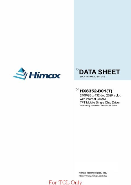
<strong>DATA</strong> <strong>SHEET</strong>( DOC No. HX8352-B01-DS )HX8352-B01(T)240RGB x 432 dot, 262K color,with internal GRAM,TFT Mobile Single Chip DriverPreliminary version 01 November, 2009
HX8352-B01(T)240RGB x 432 dot, 262K color, with internalGRAM, TFT Mobile Single Chip DriverList of ContentsNovember, 20081. General Description ............................................................................................................................... 122. Features................................................................................................................................................... 132.1 Display ........................................................................................................................................... 132.2 Display module .............................................................................................................................. 132.3 Display/control interface ................................................................................................................ 132.4 Power supply ................................................................................................................................. 142.5 Miscellaneous ................................................................................................................................ 143. Block Diagram ........................................................................................................................................ 154. Pin Description ....................................................................................................................................... 164.1 Pin description ............................................................................................................................... 164.2 Pin assignment .............................................................................................................................. 204.3 PAD coordinates ............................................................................................................................ 214.4 Alignment mark.............................................................................................................................. 284.5 Bump size ...................................................................................................................................... 295. Interface................................................................................................................................................... 315.1 System interface circuit ................................................................................................................. 325.1.1 Parallel bus system interface................................................................................................ 335.1.2 MCU data color coding ......................................................................................................... 355.1.3 Serial bus system interface .................................................................................................. 495.2 RGB interface ................................................................................................................................ 525.2.1 Color order on RGB interface............................................................................................... 565.2.2 RGB data color coding ......................................................................................................... 575.2.3 MDDI interface (mobile display digital interface) .................................................................. 606. Display Data GRAM ................................................................................................................................ 946.1 Display data GRAM mapping ........................................................................................................ 946.2 Address counter (AC) of GRAM .................................................................................................... 956.2.1 System interface to GRAM write direction............................................................................ 966.3 GRAM to display address mapping............................................................................................. 1016.3.1 Normal display on or partial Mode on, vertical scroll off..................................................... 1036.3.2 Vertical scroll display mode ................................................................................................ 1057. Functional Description ........................................................................................................................ 1087.1 Internal oscillator ......................................................................................................................... 1087.2 Gamma characteristic correction function ................................................................................... 1097.2.1 Gray voltage generator for source driver.............................................................................1107.2.2 Gray voltage generator for digital gamma correction ......................................................... 1337.3 Tearing effect output line ............................................................................................................. 1407.3.1 Tearing effect line modes.................................................................................................... 1407.3.2 Tearing effect line timing..................................................................................................... 1427.3.3 Example 1: MPU write is faster than panel read ................................................................ 1437.3.4 Example 2: MPU write is slower than panel read............................................................... 1447.4 Content adaptive brightness control (CABC) function................................................................. 1457.4.1 Module architectures .......................................................................................................... 1467.4.2 Brightness control block ..................................................................................................... 1477.4.3 Minimum brightness setting of CABC function ................................................................... 1487.4.4 Display dimming ................................................................................................................. 1487.5 Scan mode setting....................................................................................................................... 1497.6 System power on/off sequence ................................................................................................... 1507.6.1 Case 1 – NRESET line is held high or unstable by host at power on ................................ 1517.6.2 Case 2 – NRESET line is held low by host at power on .................................................... 1527.7 Free running mode specification ................................................................................................. 1537.8 LCD power generation circuit ...................................................................................................... 1567.8.1 Power supply circuit............................................................................................................ 1567.8.2 LCD power generation scheme.......................................................................................... 1587.9 Internal power on/off setting sequence ....................................................................................... 159Himax Confidential-P.1-This information contained herein is the exclusive property of Himax and shall not be distributed, reproduced, or disclosedin whole or in part without prior written permission of Himax. November, 2008
HX8352-B01(T)240RGB x 432 dot, 262K color, with internalGRAM, TFT Mobile Single Chip DriverList of ContentsNovember, 20087.10 Input / output pin state ................................................................................................................. 1627.10.1 Output pins ......................................................................................................................... 1627.10.2 Input pins ............................................................................................................................ 1628. Command .............................................................................................................................................. 1638.1 Command set .............................................................................................................................. 1638.2 Index register ............................................................................................................................... 1708.3 Display mode control register (PAGE0 - R00h)........................................................................... 1708.4 Display mode control register (PAGE0 - R01h)........................................................................... 1708.5 Column address start register (PAGE0 - R02~03h) .................................................................... 1728.6 Column address end register (PAGE0 - R04~05h) ..................................................................... 1738.7 Row address start register (PAGE0 - R06~07h) ......................................................................... 1738.8 Row address end register (PAGE0 - R08~09h) .......................................................................... 1738.9 Partial area start row register (PAGE0 - R0A~0Bh) .................................................................... 1748.10 Partial area end row register (PAGE0 - R0C~0Dh)..................................................................... 1758.11 Vertical scroll top fixed area register (PAGE0 - R0E~0Fh).......................................................... 1768.12 Vertical scroll height area register (PAGE0 - R10~11h) .............................................................. 1768.13 Vertical scroll button fixed area register (PAGE0 - R12~13h) ..................................................... 1768.14 Vertical scroll start address register (PAGE0 - R14~15h) ........................................................... 1788.15 Memory access control register (PAGE0 - R16h) ....................................................................... 1798.16 COLMOD control register (PAGE0 - R17h)................................................................................. 1808.17 OSC control register (PAGE0 - R18h & R19h)............................................................................ 1818.18 Power control 1 register (PAGE0 - R1Ah) ................................................................................... 1828.19 Power control 2 register (PAGE0 - R1Bh) ................................................................................... 1838.20 Power control 3 register (PAGE0 - R1Ch)................................................................................... 1848.21 Power control 4 register (PAGE0 - R1Dh)................................................................................... 1848.22 Power control 5 register (PAGE0 - R1Eh) ................................................................................... 1858.23 Power control 6 register (PAGE0 - R1Fh) ................................................................................... 1858.24 Read data register (PAGE0 - R22h) ............................................................................................ 1878.25 VCOM control 1~3 register (PAGE0 - R23~25h)......................................................................... 1878.26 Display control 1~3 register (PAGE0 - R26h~R28h) ................................................................... 1908.27 Frame control 1~4 register (PAGE0 - R29h~R2Ch).................................................................... 1938.28 Cycle control 1~2 register (PAGE0 - R2Dh~R2Eh)..................................................................... 1958.29 Display inversion register (PAGE0 - R2Fh) ................................................................................. 1968.30 RGB interface control 1~4 register (PAGE0 - R31h~R34h) ........................................................ 1968.31 OTP contril 1~4 register (PAGE0 - R38h ~ R3Bh) ...................................................................... 1988.32 CABC control 1~4 register (PAGE0 - R3Ch~3Fh)....................................................................... 1998.33 Gamma control 1~35 register (PAGE0 - R40h~5Dh) .................................................................. 2018.34 TE mode control (PAGE0 - R60h) ............................................................................................... 2068.35 ID1~4 register (PAGE0 - R61h~64h)........................................................................................... 2078.36 MDDI control 4~5 register (PAGE0 - R68h~R69h)...................................................................... 2088.37 GPIO control 1~5 register (PAGE0 - R6Bh~R6Fh) ..................................................................... 2088.38 SUB_PANEL control 1~4 register (PAGE0 - R70h~R73h).......................................................... 2108.39 Column address counter 2~1 register (PAGE0 - R80h~R81h) ....................................................2118.40 Row address counter 2~1 register (PAGE0 - R82h~R83h)......................................................... 2128.41 Set TE output delay line resgiter2~1 (R84~R85h) ...................................................................... 2138.42 OTP Control 5~6 (R87h).............................................................................................................. 2148.43 Command page select register (RFFh) ....................................................................................... 2148.44 DGC control register (PAGE1 – R00h)........................................................................................ 2148.45 DGC LUT1~192 register (PAGE1 – R01h~C0h) ......................................................................... 2158.46 CABC control 5~7 register (PAGE1 – RC3h, RC5h, RC7h)........................................................ 2158.47 Gain select register 0~8 (PAGE1 – RCBh~D3h)......................................................................... 2168.48 Power saving counter 1~4 (PAGE0 – RE4h~E7h) ...................................................................... 2189. Layout Recommendation .................................................................................................................... 2209.1 Maximum layout resistance ......................................................................................................... 2219.2 External components connection ................................................................................................ 222Himax ConfidentialThis information contained herein is the exclusive property of Himax and shall not be distributed, reproduced, or disclosedin whole or in part without prior written permission of Himax.-P.2-November, 2008
HX8352-B01(T)240RGB x 432 dot, 262K color, with internalGRAM, TFT Mobile Single Chip DriverList of ContentsNovember, 200810. OTP Programming................................................................................................................................ 22310.1 OTP table..................................................................................................................................... 22310.2 OTP programming flow................................................................................................................ 22510.3 OTP programming sequence ...................................................................................................... 22710.4 OTP Read flow ............................................................................................................................ 22810.5 OTP read sequence..................................................................................................................... 22910.6 Programming circuitry.................................................................................................................. 22911. Electrical Characteristics .................................................................................................................... 23011.1 Absolute maximum ratings .......................................................................................................... 23011.2 ESD protection level .................................................................................................................... 23011.3 DC characteristics ....................................................................................................................... 23111.4 AC characteristics........................................................................................................................ 23311.4.1 Parallel interface characteristics (8080-series MPU) ......................................................... 23311.4.2 Serial interface characteristics ........................................................................................... 23511.4.3 RGB interface characteristics............................................................................................. 23611.4.4 Reset input timing............................................................................................................... 23911.4.5 MDDI interface characteristics ........................................................................................... 24012. Ordering Information............................................................................................................................ 24113. Revision History ................................................................................................................................... 241Himax ConfidentialThis information contained herein is the exclusive property of Himax and shall not be distributed, reproduced, or disclosedin whole or in part without prior written permission of Himax.-P.3-November, 2008
HX8352-B01(T)240RGB x 432 dot, 262K color, with internalGRAM, TFT Mobile Single Chip DriverList of Figures November, 2008Himax ConfidentialFigure 5.1 Register read/write timing in parallel bus system interface (for I80 series MPU) ............ 33Figure 5.2 GRAM read/write timing in parallel bus system interface (for I80 series MPU)............... 34Figure 5.3 Example of I80- system 18-bit parallel bus interface....................................................... 37Figure 5.4 Input data bus and GRAM data mapping in 18-bit bus system interface with 18 bit-datainput (“BS3, BS2, BS1, BS0”=”1010” or “1000”)........................................................................ 37Figure 5.5 Example of I80 system 16-bit parallel bus interface type I .............................................. 38Figure 5.6 Example of I80 system 16-bit parallel bus interface type II ............................................. 38Figure 5.7 Input data bus and GRAM data mapping in 16-bit bus system interface with 12 bit-datainput (R17H=03h and “BS3, BS2, BS1, BS0”=”0000”) .............................................................. 39Figure 5.8 Input data bus and GRAM data mapping in 16-bit bus system interface with 12 bit-datainput (R17H=04h and “BS3, BS2, BS1, BS0”=”0000”) .............................................................. 39Figure 5.9 Input data bus and GRAM data mapping in 16-bit bus system interface with 16 bit-datainput (R17H=05h and “BS3, BS2, BS1, BS0”=”0000”) .............................................................. 39Figure 5.10 Input data bus and GRAM data mapping in 16-bit bus system interface with 18(12+6)bit-data input (R17H=06h and “BS3, BS2, BS1, BS0”=”0000”) .................. 錯 誤 ! 尚 未 定 義 書 籤 。Figure 5.11 Input data bus and GRAM data mapping in 16-bit bus system interface with 18(16+2)bit-data input (R17H=07h and “BS3,BS2, BS1, BS0”=”0000”) .................................................. 39Figure 5.12 Input data bus and GRAM data mapping in 16-bit bus system interface with 12 bit-datainput (R17H=03h and “BS3, BS2, BS1, BS0”=”0010”) .............................................................. 40Figure 5.13 Input data bus and GRAM data mapping in 16-bit bus system interface with 12 bit-datainput (R17H=04h and “BS3, BS2, BS1, BS0”=”0010”) .............................................................. 40Figure 5.14 Input data bus and GRAM data mapping in 16-bit bus system interface with 16 bit-datainput (R17H=05h and “BS3, BS2, BS1, BS0”=”0010”) .............................................................. 40Figure 5.15 Input data bus and GRAM data mapping in 16-bit bus system interface with 18(12+6)bit-data input (R17H=06h and “BS3, BS2, BS1, BS0”=”0010”) ................................................. 40Figure 5.16 Input data bus and GRAM data mapping in 16-bit bus system interface with 18(16+2)bit-data input (R17H=07h and “BS3, BS2, BS1, BS0”=”0010”) ................................................. 41Figure 5.17 Example of I80 system 9-bit parallel bus interface type I .............................................. 42Figure 5.18 Example of I80 system 9-bit parallel bus interface type II ............................................. 42Figure 5.19 Input data bus and GRAM data mapping in 9-bit bus system interface with 18 bit-datainput (R17H=06h and “BS3, BS2, BS1, BS0”=”1001”) .............................................................. 43Figure 5.20 Input data bus and GRAM data mapping in 9-bit bus system interface with 18 bit-datainput (R17H=06h and “BS3, BS2, BS1, BS0”=”1011”) .............................................................. 43Figure 5.21 Example of I80-system 8-bit parallel bus interface type I .............................................. 44Figure 5.22 Example of I80-system 8-bit parallel bus interface type II ............................................. 44Figure 5.23 Input data bus and GRAM data mapping in 8-bit bus system interface with 12 bit-datainput (R17H=03h and“BS3, BS2, BS1, BS0”=”0001”) ............................................................... 45Figure 5.24 Input data bus and GRAM data mapping in 8-bit bus system interface with 16 bit-datainput (R17H=05h and “BS3, BS2, BS1, BS0”=”0001”) .............................................................. 45Figure 5.25 Input data bus and GRAM data mapping in 8-bit bus system interface with 18 bit-datainput (R17H=06h and “BS3, BS2, BS1, BS0”=”0001”) .............................................................. 45Figure 5.26 Input data bus and GRAM data mapping in 8-bit bus system interface with 12 bit-datainput (R17H=03h and“BS3, BS2, BS1, BS0”=”0011”) ............................................................... 46Figure 5.27 Input data bus and GRAM data mapping in 8-bit bus system interface with 16 bit-datainput (R17H=05h and “BS3, BS2, BS1, BS0”=”0011”) .............................................................. 46Figure 5.28 Input data bus and GRAM data mapping in 8-bit bus system interface with 18 bit-datainput (R17H=06h and “BS3, BS2, BS1, BS0”=”0011”) .............................................................. 46Figure 5.29 Index register read/write timing in 3-wire serial bus system interface ........................... 49Figure 5.30 Data write timing in 3-wire serial bus system interface.................................................. 50Figure 5.31 Index register write timing in 4-wire serial bus system interface ................................... 50Figure 5.32 Data write timing in 4-wire serial bus system interface.................................................. 51Figure 5.33 DOTCLK cycle ............................................................................................................... 52Figure 5.34 RGB interface circuit input timing diagram .................................................................... 53Figure 5.35 RGB mode timing diagram ............................................................................................ 54Figure 5.36 RGB 18-bit/pixel on 6-bit data width .............................................................................. 57This information contained herein is the exclusive property of Himax and shall not be distributed, reproduced, or disclosedin whole or in part without prior written permission of Himax.-P.4-November, 2008
HX8352-B01(T)240RGB x 432 dot, 262K color, with internalGRAM, TFT Mobile Single Chip DriverList of Figures November, 2008Himax ConfidentialFigure 5.37 RGB 16-bit/pixel on 16-bit data width ............................................................................ 58Figure 5.38 RGB 18-bit/pixel on 18-bit data width ............................................................................ 59Figure 5.39 Physical connection of MDDI host and client ................................................................ 60Figure 5.40 MDDI terminology .......................................................................................................... 61Figure 5.41 Example of bi-directional MDDI communication............................................................ 61Figure 5.42 Data-STB encoding........................................................................................................ 62Figure 5.43 Data / STB generation & recovery circuit....................................................................... 62Figure 5.44 Differential connection between host and client ............................................................ 63Figure 5.45 MDDI packet structure ................................................................................................... 64Figure 5.46 Panel read is faster than MPU write .............................................................................. 67Figure 5.47 Panel read is slower than MPU write............................................................................. 68Figure 5.48 MDDI transceiver / receiver state in hibernation............................................................ 69Figure 5.49 Host-initiated link wakeup sequence ............................................................................. 70Figure 5.50 Client-initiated link wake-up sequence .......................................................................... 71Figure 5.51 MDDI operation mode.................................................................................................... 78Figure 5.52 Sub panel interface ........................................................................................................ 80Figure 5.53 Main/sub panel selection procedure .............................................................................. 81Figure 5.54 18-/16-bit sub panel interface register access data timing for I80 series TFT sub panel................................................................................................................................................... 82Figure 5.55 9-/8-bit sub panel interface register access data timing for I80 series TFT sub panel .. 82Figure 5.56 18-/16-bit sub panel interface register access data timing for I80 series TFT sub panel................................................................................................................................................... 83Figure 5.57 9-/8-bit sub panel interface register access data timing for M68 series TFT sub panel 83Figure 5.58 18-bit sub panel interface video data timing for I80 series TFT sub panel .................... 84Figure 5.59 18-bit sub panel interface video data timing for M68 series TFT sub panel .................. 84Figure 5.60 16-bit sub panel interface video data timing for I80 series TFT sub panel .................... 85Figure 5.61 16-bit sub panel interface video data timing for M68 series TFT sub panel .................. 85Figure 5.62 9-bit sub panel interface video data timing for I80 series TFT sub panel ...................... 86Figure 5.63 9-bit sub panel interface video data timing for M68 series TFT sub panel .................... 86Figure 5.64 8-bit sub panel interface video data timing for I80 series TFT sub panel ...................... 87Figure 5.65 8-bit sub panel interface video data timing for M68 series TFT sub panel .................... 87Figure 5.66 18-/16-bit sub panel interface register access data timing for I80 series STN sub panel................................................................................................................................................... 88Figure 5.67 9-/8-bit sub panel interface register access data timing for I80 series STN sub panel . 88Figure 5.68 18-/16-bit sub panel interface register access data timing for M68 series STN sub panel................................................................................................................................................... 89Figure 5.69 9-/8-bit sub panel interface register access data timing for M68 series STN sub panel 89Figure 5.70 18-bit sub panel interface video data timing for I80 series STN sub panel ................... 90Figure 5.71 18-bit sub panel interface video data timing for M68 series STN sub panel ................. 90Figure 5.72 16-bit sub panel interface video data timing for I80 series STN sub panel ................... 91Figure 5.73 16-bit sub panel interface video data timing for M68 series STN sub panel ................. 91Figure 5.74 9-bit sub panel interface video data timing for I80 series STN sub panel ..................... 92Figure 5.75 9-bit sub panel interface video data timing for M68 series STN sub panel ................... 92Figure 5.76 8-bit sub panel interface video data timing for I80 series STN sub panel ..................... 93Figure 5.77 8-bit sub panel interface video data timing for M68 series STN sub panel ................... 93Figure 6.1 Image data sending order from host................................................................................ 96Figure 6.2 MY, MX, MV setting of 240RGB x 432 dot ...................................................................... 96Figure 6.3 Example for rotation with MY, MX and MV – 1................................................................ 99Figure 6.4 Example for rotation with MY, MX and MV - 2............................................................... 100Figure 6.5 Partial display area setting (240x432 panel).................................................................. 104Figure 6.6 Vertical scrolling ............................................................................................................. 105Figure 6.7 Memory map of vertical scrolling 1 ................................................................................ 105Figure 6.8 Memory map of vertical scrolling 2 ................................................................................ 106Figure 6.9 Memory map of vertical scrolling 3 ................................................................................ 106Figure 6.10 Vertical scrolling example ............................................................................................ 107This information contained herein is the exclusive property of Himax and shall not be distributed, reproduced, or disclosedin whole or in part without prior written permission of Himax.-P.5-November, 2008
HX8352-B01(T)240RGB x 432 dot, 262K color, with internalGRAM, TFT Mobile Single Chip DriverList of Figures November, 2008Himax ConfidentialFigure 7.1 HX8352-B01 internal clock circuit.................................................................................. 108Figure 7.2 Gamma adjustments different of source driver with digital gamma correction.............. 109Figure 7.3 Grayscale control ............................................................................................................110Figure 7.4 Structure of grayscale voltage generator ........................................................................ 111Figure 7.5 Gamma resister stream and gamma reference voltage .................................................113Figure 7.6 Relationship between source output and Vcom ............................................................ 132Figure 7.7 Relationship between GRAM data and output level (normal white panel INVON=“0”) . 132Figure 7.8 Block diagram of digital gamma correction.................................................................... 133Figure 7.9 TE Mode 1 output .......................................................................................................... 140Figure 7.10 TE Mode 2 output ........................................................................................................ 141Figure 7.11 TE Mode 2 output......................................................................................................... 141Figure 7.12 Waveform of tearing effect signal ................................................................................ 142Figure 7.13 Timing of tearing effect signal...................................................................................... 142Figure 7.14 Timing of MPU write is faster than panel read ............................................................. 143Figure 7.15 Display of MPU write is faster than panel read............................................................ 143Figure 7.16 Timing of MPU write is slower than panel read ........................................................... 144Figure 7.17 Display of MPU write is slower than panel read .......................................................... 144Figure 7.18 Example of CABC function .......................................................................................... 145Figure 7.19 CABC block diagram.................................................................................................... 145Figure 7.20 CABC_PWM_OUT output duty.................................................................................... 147Figure 7.21 Dimming function ......................................................................................................... 148Figure 7.22 Gate scan mode........................................................................................................... 149Figure 7.23 Case 1 –NRESET line is held high or unstable by host at power on........................... 151Figure 7.24 Case 2 –NRESET line is held low by host at power on............................................... 152Figure 7.25 Power on sequence of FR-mode (for normally-white panel) ....................................... 154Figure 7.26 Power off sequence of FR-mode ................................................................................. 154Figure 7.27 Block diagram of HX8352-B01 power circuit ............................................................... 156Figure 7.28 LCD power generation scheme ................................................................................... 158Figure 7.29 Display on/off set flow .................................................................................................. 159Figure 7.30 Standby mode setting flow........................................................................................... 160Figure 7.31 Power supply setting flow ............................................................................................ 161Figure 8.1 Index register ................................................................................................................. 170Figure 8.2 Himax ID register (PAGE0 - R00h) ................................................................................ 170Figure 8.3 Display mode control register (PAGE0 - R01h) ............................................................. 170Figure 8.4 Column address start register upper byte (PAGE0 - R02h) .......................................... 172Figure 8.5 Column address start register low byte (PAGE0 - R03h) .............................................. 172Figure 8.6 Column address end register upper byte (PAGE0 - R04h) ........................................... 173Figure 8.7 Column address end register low byte (PAGE0 - R05h) ............................................... 173Figure 8.8 Row address start register upper byte (PAGE0 - R06h) ............................................... 173Figure 8.9 Row address start register low byte (PAGE0 - R07h) ................................................... 173Figure 8.10 Row address end register upper byte (PAGE0 - R08h) .............................................. 173Figure 8.11 Row address end register low byte (PAGE0 - R09h) .................................................. 173Figure 8.12 Partial area start row register upper byte (PAGE0 - R0Ah)......................................... 174Figure 8.13 Partial area start row register low byte (PAGE0 - R0Bh)............................................. 174Figure 8.14 Partial area end row register upper byte (PAGE0 - R0Ch).......................................... 175Figure 8.15 Partial area end row register low byte (PAGE0 - R0Dh) ............................................. 175Figure 8.16 Vertical scroll top fixed area register upper byte (PAGE0 - R0Eh).............................. 176Figure 8.17 Vertical scroll top fixed area register low byte (PAGE0 - R0Fh).................................. 176Figure 8.18 Vertical scroll height area register upper byte (PAGE0 - R10h).................................. 176Figure 8.19 Vertical scroll height area register low byte (PAGE0 - R11h)...................................... 176Figure 8.20 Vertical scroll button fixed area register upper byte (PAGE0 - R12h) ......................... 176Figure 8.21 Vertical scroll button fixed area register low byte (PAGE0 - R13h)............................. 176Figure 8.22 Vertical scroll start address register upper byte (PAGE0 - R14h) ............................... 178Figure 8.23 Vertical scroll start address register low byte (PAGE0 - R15h) ................................... 178Figure 8.24 Memory access control register (PAGE0 - R16h) ....................................................... 179This information contained herein is the exclusive property of Himax and shall not be distributed, reproduced, or disclosedin whole or in part without prior written permission of Himax.-P.6-November, 2008
HX8352-B01(T)240RGB x 432 dot, 262K color, with internalGRAM, TFT Mobile Single Chip DriverList of Figures November, 2008Himax ConfidentialFigure 8.25 COLMOD control register (PAGE0 - R17h)................................................................. 180Figure 8.26 OSC control 1 register (PAGE0 - R18h) ...................................................................... 181Figure 8.27 OSC control 2 register (PAGE0 - R19h) ...................................................................... 181Figure 8.28 Power control 1 register (PAGE0 - R1Ah) ................................................................... 182Figure 8.29 Power control 2 register (PAGE0 - R1Bh) ................................................................... 183Figure 8.30 Power control 3 register (PAGE0 - R1Ch) ................................................................... 184Figure 8.31 Power control 4 register (PAGE0 - R1Dh) ................................................................... 184Figure 8.32 Power control 5 register (PAGE0 - R1Eh) ................................................................... 185Figure 8.33 Power control 6 register (PAGE0 - R1Fh) ................................................................... 185Figure 8.34 Read data register (PAGE0 - R22h) ............................................................................ 187Figure 8.35 Vcom control 1 register (PAGE0 - R23h)..................................................................... 187Figure 8.36 Vcom control 2 register (PAGE0 - R24h)..................................................................... 187Figure 8.37 Vcom control 3 register (PAGE0 - R25h)..................................................................... 187Figure 8.38 Display control 1 register (PAGE0 - R26h).................................................................. 190Figure 8.39 Display control 2 register (PAGE0 - R27h).................................................................. 190Figure 8.40 Display control 3 register (PAGE0 - R28h).................................................................. 190Figure 8.41 Frame control 1 register (PAGE0 - R29h) ................................................................... 193Figure 8.42 Frame control 2 register (PAGE0 - R2Ah) ................................................................... 193Figure 8.43 Frame control 3 register (PAGE0 - R2Bh) ................................................................... 193Figure 8.44 Frame control 4 register (PAGE0 - R2Ch)................................................................... 193Figure 8.45 Cycle control 1 register (PAGE0 - R2Dh) .................................................................... 195Figure 8.46 Cycle control 2 register (PAGE0 - R2Eh) .................................................................... 195Figure 8.47 Display inversion control register (PAGE0 - R2Fh) ..................................................... 196Figure 8.48 RGB interface control 1 register (PAGE0 - R31h) ....................................................... 196Figure 8.49 RGB interface control 2 register (PAGE0 - R32h) ....................................................... 196Figure 8.50 RGB interface control 3 register (PAGE0 - R33h) ....................................................... 196Figure 8.51 RGB interface control 4 register (PAGE0 - R34h) ....................................................... 196Figure 8.52 OTP control 1 register (PAGE0 - R38h) ...................................................................... 198Figure 8.53 OTP control 2 register (PAGE0 - R39h) ...................................................................... 198Figure 8.54 OTP control 3 register (PAGE0 - R3Ah) ...................................................................... 198Figure 8.55 OTP control 4 register (PAGE0 - R3Bh) ...................................................................... 198Figure 8.56 CABC control 1 register (PAGE0 - R3Ch) ................................................................... 199Figure 8.57 CABC control 2 register (PAGE0 - R3Dh) ................................................................... 199Figure 8.58 CABC control 3 register (PAGE0 - R3Eh).................................................................... 199Figure 8.59 CABC control 4 register (PAGE0 - R3Fh).................................................................... 199Figure 8.60 Gamma control 1 register (PAGE0 - R40h) ................................................................. 201Figure 8.61 Gamma control 2 register (PAGE0 - R41h) ................................................................. 201Figure 8.62 Gamma control 3 register (PAGE0 - R42h) ................................................................. 201Figure 8.63 Gamma control 4 register (PAGE0 - R43h) ................................................................. 201Figure 8.64 Gamma control 5 register (PAGE0 - R44h) ................................................................. 201Figure 8.65 Gamma control 6 register (PAGE0 - R45h) ................................................................. 201Figure 8.66 Gamma control 7 register (PAGE0 - R46h) ................................................................. 202Figure 8.67 Gamma control 8 register (PAGE0 - R47h) ................................................................. 202Figure 8.68 Gamma control 9 register (PAGE0 - R48h) ................................................................. 202Figure 8.69 Gamma control 10 register (PAGE0 - R49h) ............................................................... 202Figure 8.70 Gamma control 11 register (PAGE0 - R4Ah) ............................................................... 202Figure 8.71 Gamma control 12 register (PAGE0 - R4Bh)............................................................... 202Figure 8.72 Gamma control 13 register (PAGE0 - R4Ch)............................................................... 203Figure 8.73 Gamma control 17 register (PAGE0 - R50h) ............................................................... 203Figure 8.74 Gamma control 18 register (PAGE0 - R51h) ............................................................... 203Figure 8.75 Gamma control 19 register (PAGE0 - R52h) ............................................................... 203Figure 8.76 Gamma control 20 register (PAGE0 - R53h) ............................................................... 203Figure 8.77 Gamma control 21 register (PAGE0 - R54h) ............................................................... 203Figure 8.78 Gamma control 22 register (PAGE0 - R55h) ............................................................... 204Figure 8.79 Gamma control 23 register (PAGE0 - R56h) ............................................................... 204This information contained herein is the exclusive property of Himax and shall not be distributed, reproduced, or disclosedin whole or in part without prior written permission of Himax.-P.7-November, 2008
HX8352-B01(T)240RGB x 432 dot, 262K color, with internalGRAM, TFT Mobile Single Chip DriverList of Figures November, 2008Himax ConfidentialFigure 8.80 Gamma control 24 register (PAGE0 - R57h) ............................................................... 204Figure 8.81 Gamma control 25 register (PAGE0 - R58h) ............................................................... 204Figure 8.82 Gamma control 26 register (PAGE0 - R59h) ............................................................... 204Figure 8.83 Gamma control 27 register (PAGE0 - R5Ah)............................................................... 204Figure 8.84 Gamma control 28 register (PAGE0 - R5Bh)............................................................... 205Figure 8.85 Gamma control 29 register (PAGE0 - R5Ch)............................................................... 205Figure 8.86 Gamma control 30 register (PAGE0 - R5Dh)............................................................... 205Figure 8.87 Mode control register (PAGE0 - R60h) ........................................................................ 206Figure 8.88 ID1 register (PAGE0 - R61h) ....................................................................................... 207Figure 8.89 ID3 register (PAGE0 - R62h) ....................................................................................... 207Figure 8.90 ID3 register (PAGE0 - R63h) ....................................................................................... 207Figure 8.91 ID4 register (PAGE0 - R64h) ....................................................................................... 207Figure 8.92 MDDI control 4 register (PAGE0 - R68h)..................................................................... 208Figure 8.93 MDDI control 5 register (PAGE0 - R69h)..................................................................... 208Figure 8.94 GPIO control 1 register (PAGE0 - R6Bh)..................................................................... 208Figure 8.95 GPIO control 2 register (PAGE0 - R6Ch) .................................................................... 208Figure 8.96 GPIO control 3 register (PAGE0 - R6Dh) .................................................................... 209Figure 8.97 GPIO control 4 register (PAGE0 – R6Eh).................................................................... 209Figure 8.98 GPIO control 5 register (PAGE0 – R6Fh) .................................................................... 209Figure 8.99 SUB_PANEL control 1 register (PAGE0 - R70h) ......................................................... 210Figure 8.100 SUB_PANEL control 2 register (PAGE0 - R71h) ....................................................... 210Figure 8.101 SUB_PANEL control 3 register (PAGE0 - R72h) ....................................................... 210Figure 8.102 SUB_PANEL control 4 register (PAGE0 - R73h) ....................................................... 210Figure 8.103 Column address counter 2 register (PAGE0 - R80h) .................................................211Figure 8.104 Column address counter 1 register (PAGE0 - R81h) .................................................211Figure 8.105 Row address counter 2 register (PAGE0 - R82h)...................................................... 212Figure 8.106 Row address counter 1 register (PAGE0 - R83h)...................................................... 212Figure 8.107 Row address counter 2 register (PAGE0 - R84h)...................................................... 213Figure 8.108 Row address counter 1 register (PAGE0 - R85h)...................................................... 213Figure 8.109 OTP Control 6 register (PAGE0 - R87h).................................................................... 214Figure 8.110 Command page select 2 register (RFFh) .................................................................. 214Figure 8.111 DGC control register (PAGE1 – R00h) ...................................................................... 214Figure 8.112 CABC control 5 (PAGE1 – RC3h).............................................................................. 215Figure 8.113 CABC control 6 (PAGE1 – RC5h).............................................................................. 215Figure 8.114 CABC control 7 (PAGE1 – RC7h).............................................................................. 215Figure 8.115 Gain select register 0 (PAGE1 – RCBh) .................................................................... 216Figure 8.116 Gain select register 1 (PAGE1 – RCCh).................................................................... 216Figure 8.117 Gain select register 2 (PAGE1 – RCDh).................................................................... 216Figure 8.118 Gain select register 3 (PAGE1 – RCEh) .................................................................... 216Figure 8.119 Gain select register 4 (PAGE1 – RCFh) .................................................................... 216Figure 8.120 Gain select register 5 (PAGE1 – RD0h) .................................................................... 216Figure 8.121 Gain select register 6 (PAGE1 – RD1h) .................................................................... 217Figure 8.122 Gain select register 7 (PAGE1 – RD2h) .................................................................... 217Figure 8.123 Gain select register 8 (PAGE1 – RD3h) .................................................................... 217Figure 8.124 Power saving register 1 (PAGE0 – RE4h) ................................................................. 218Figure 8.125 Power saving register 2 (PAGE0 – RE5h) ................................................................. 218Figure 8.126 Power saving register 3 (PAGE0 – RE6h) ................................................................. 218Figure 8.127 Power saving register 4 (PAGE0 – RE7h) ................................................................. 218Figure 9.1 ayout Recommendation of HX8352-B01 ....................................................................... 220Figure 10.1 OTP programming sequence....................................................................................... 225Figure 10.2 OTP programming example for ID1~ID4 ..................................................................... 226Figure 10.3 OTP read example for ID1........................................................................................... 228Figure 11.1 Parallel interface characteristics (8080-series MPU) ................................................... 233Figure 11.2 Chip select timing......................................................................................................... 234Figure 11.3 Write to read and read to write timing .......................................................................... 234This information contained herein is the exclusive property of Himax and shall not be distributed, reproduced, or disclosedin whole or in part without prior written permission of Himax.-P.8-November, 2008
HX8352-B01(T)240RGB x 432 dot, 262K color, with internalGRAM, TFT Mobile Single Chip DriverList of Figures November, 2008Figure 11.4 Serial interface characteristics ..................................................................................... 235Figure 11.5 RGB interface characteristics....................................................................................... 236Figure 11.6 Reset input timing ........................................................................................................ 239Figure 11.7 MDDI interface characteristics ..................................................................................... 240Himax ConfidentialThis information contained herein is the exclusive property of Himax and shall not be distributed, reproduced, or disclosedin whole or in part without prior written permission of Himax.-P.9-November, 2008
HX8352-B01(T)240RGB x 432 dot, 262K color, with internalGRAM, TFT Mobile Single Chip DriverList of Tables November, 2008Himax ConfidentialTable 5.1 Input bus format selection of system interface circuit ....................................................... 32Table 5.2 Data pin function for I80 series CPU ................................................................................. 33Table 5.3 8-bit parallel interface type I GRAM write table ................................................................. 35Table 5.4 16-bit parallel interface type I GRAM write table ............................................................... 35Table 5.5 9-bit parallel interface type I GRAM write table ................................................................. 35Table 5.6 18-bit parallel interface type I GRAM write table ............................................................... 35Table 5.7 8-bit parallel interface type II GRAM write table ................................................................ 36Table 5.8 16-bit parallel interface type II GRAM write table .............................................................. 36Table 5.9 9-bit parallel interface set type II GRAM write table .......................................................... 36Table 5.10 18-bit parallel interface type II GRAM write set table ...................................................... 36Table 5.11 8-bit parallel interface type I GRAM read table................................................................ 47Table 5.12 16-bit parallel interface type I GRAM read table ............................................................. 47Table 5.13 9-bit parallel interface type I GRAM read table ............................................................... 47Table 5.14 18-bit parallel interface type I GRAM read table ............................................................. 47Table 5.15 8-bit parallel interface type II GRAM read table .............................................................. 48Table 5.16 16-bit parallel interface type II GRAM read table ............................................................ 48Table 5.17 9-bit parallel interface type II GRAM read table .............................................................. 48Table 5.18 18-bit parallel interface type II GRAM read table ............................................................ 48Table 5.19 Function of RS and R/W bit bus ...................................................................................... 49Table 5.20 RGB interface bus width set table ................................................................................... 55Table 5.21 Meaning of pixel information for main colors on RGB interface...................................... 56Table 5.22 List of supported MDDI packet ........................................................................................ 64Table 5.23 GPIO control related register........................................................................................... 75Table 5.24 Operation mode list ......................................................................................................... 79Table 6.1 GRAM address for display panel position (240 X 432) ..................................................... 94Table 6.2 Address counter range ...................................................................................................... 95Table 6.3 CASET and PASET control for physical column/page pointers ........................................ 96Table 6.4 Rules for updating GRAM order ........................................................................................ 97Table 6.5 Address direction settings ................................................................................................. 98Table 6.6 GRAM X address and display panel position (240RGBx432 dot)................................... 101Table 6.7 GRAM address and display panel position (GS=L, 240RGBx432 dot)........................... 102Table 6.8 GRAM address and display panel position (GS=H , 240RGBx432 dot) ......................... 102Table 6.9 ISC[3:0] bits definition...................................................................................................... 104Table 7.1 Gamma-adjustment registers ...........................................................................................112Table 7.2 Offset adjustment 0~5 ......................................................................................................114Table 7.3 Center adjustment ............................................................................................................114Table 7.4 Voltage calculation formula for VinP/N 0..........................................................................115Table 7.5 Voltage calculation formula for VinP/N 1..........................................................................116Table 7.6 Voltage calculation formula for VinP/N 2..........................................................................117Table 7.7 Voltage calculation formula for VinP/N 3..........................................................................118Table 7.8 Voltage calculation formula for VinP/N 4......................................................................... 120Table 7.9 Voltage calculation formula for VinP/N 5......................................................................... 121Table 7.10 Voltage calculation formula for VinP/N 6....................................................................... 122Table 7.11 Voltage calculation formula for VinP/N 7 ....................................................................... 123Table 7.12 Voltage calculation formula for VinP/N 8....................................................................... 125Table 7.13 Voltage calculation formula for VinP/N 9....................................................................... 126Table 7.14 Voltage calculation formula for VinP/N 10..................................................................... 127Table 7.15 Voltage calculation formula for VinP/N 11..................................................................... 128Table 7.16 Voltage calculation formula for VinP/N 12..................................................................... 129Table 7.17 Voltage calculation formula of 64-grayscale voltage (positive polarity) ........................ 130Table 7.18 Voltage calculation formula of grayscale voltage V2~V7 and V56~V61 ....................... 130Table 7.19 Voltage calculation formula of 64-grayscale voltage (negative polarity) ....................... 131Table 7.20 Voltage calculation formula of grayscale voltage V2~V7 and V56~V61 ....................... 131Table 7.21 DGLUT for red color (1)................................................................................................. 134Table 7.22 DGLUT for red color (2)................................................................................................. 135This information contained herein is the exclusive property of Himax and shall not be distributed, reproduced, or disclosedin whole or in part without prior written permission of Himax.-P.10-November, 2008
HX8352-B01(T)240RGB x 432 dot, 262K color, with internalGRAM, TFT Mobile Single Chip DriverList of Tables November, 2008Table 7.23 DGLUT for green color (1)............................................................................................. 136Table 7.24 DGLUT for green color (2)............................................................................................. 137Table 7.25 DGLUT for blue color (1) ............................................................................................... 138Table 7.26 DGLUT for blue color (2) ............................................................................................... 139Table 7.27 AC characteristics of tearing effect signal ..................................................................... 142Table 7.28 Pin information of free running mode ............................................................................ 153Table 7.29 Frequency definition of free running mode display ....................................................... 155Table 7.30 Adoptability of capacitor................................................................................................. 157Table 7.31 Characteristics of output pins........................................................................................ 162Table 7.32 Characteristics of input pins.......................................................................................... 162Table 8.1 List table of command set page 0 ................................................................................... 165Table 8.2 List table of command set page 1 ................................................................................... 169Table 8.3 Power control 8 register................................................................................................... 181Table 9.1 Maximum layout resistance ............................................................................................. 221Table 11.1 Absolute maximum ratings............................................................................................. 230Table 11.2 ESD protection level ...................................................................................................... 230Table 11.3 DC characteristics.......................................................................................................... 231Table 11.4 MDDI DC characteristics ............................................................................................... 232Himax ConfidentialThis information contained herein is the exclusive property of Himax and shall not be distributed, reproduced, or disclosedin whole or in part without prior written permission of Himax.-P.11-November, 2008
HX8352-B01(T)240RGB x 432 dot, 262K color, with internalGRAM, TFT Mobile Single Chip DriverPreliminary Version 01 November, 20081. General DescriptionThis document describes HX8352-B01 240RGBx432 dots resolution driving controller.The HX8352-B01 is designed to provide a single-chip solution that combines a gatedriver, a source driver, power supply circuit for 262,144 colors to drive a TFT panelwith 240RGBx432 dots at maximum.The HX8352-B01 can be operated in low-voltage (1.65V) condition for the interfaceand integrated internal boosters that produce the liquid crystal voltage, breederresistance and the voltage follower circuit for liquid crystal driver. In addition, TheHX8352-B01 also supports various functions to reduce the power consumption of aLCD system via software control.The HX8352-B01 is suitable for any small portable battery-driven and long-termdriving products, such as small PDAs, digital cellular phones and bi-directionalpagers.Himax Confidential-P.12-This information contained herein is the exclusive property of Himax and shall not be distributed, reproduced, or disclosedin whole or in part without prior written permission of Himax. November, 2008
HX8352-B01(T)240RGB x 432 dot, 262K color, TFT Mobile Single Chip Driver2. Features<strong>DATA</strong> <strong>SHEET</strong> Preliminary V012.1 Display• Resolution:• 240(H) x RGB(H) x 320(V)• 240(H) x RGB(H) x 400(V)• 240(H) x RGB(H) x 432(V)• Display Color modes• Normal Display Mode On1. System Interface Circuita. 4,096(R(4),G(4),B(4)) colorsb. 65,536(R(5),G(6),B(5)) colorsc. 262,144(R(6),G(6),B(6)) colors2. RGB Interface Circuit1. 65,536(R(5),G(6),B(5)) colors2. 262,144(R(6),G(6),B(6)) colors• Idle Mode On− 8 (R(1),G(1),B(1)) colors• Display color modes• Full color mode:− 262k colours (18bit 6(R):6(G):6(B))• Reduce color mode:− 65k colours (16bit 5(R):6(G):5(B))- 4096 colours(12bit 4(R):4(G):4(B))2.2 Display module• On module VCOM control (-2.0 to 5.5V Common electrode output voltage range)• On module DC/DC converter• VLCD = 4.6 to 6.0V (Source output voltage range)• VGH = +9.0 to +16.5V (Positive Gate output voltage range)• VGL = -6.0 to -13.5V (Negative Gate output voltage range)• Frame Memory area 240(H) x 432(V) x 18bit2.3 Display/control interface• Display Interface types supported• System interface:a. 8-/9-/16-/18-bit parallel bus system interfaceb. 3-/4-wire serial bus system interface• RGB interface:a. 6-/16-/18-bit RGB interface• MDDI (Mobile Display Digital Interface) interfaceHimax ConfidentialThis information contained herein is the exclusive property of Himax and shall not be distributed, reproduced, or disclosedin whole or in part without prior written permission of Himax.-P.13-November, 2008
HX8352-B01(T)240RGB x 432 dot, 262K color, TFT Mobile Single Chip Driver• Color modes• 12 bit/pixel: R(4), G(4), B(4)• 16 bit/pixel: R(5), G(6), B(5)• 18 bit/pixel: R(6), G(6), B(6))<strong>DATA</strong> <strong>SHEET</strong> Preliminary V012.4 Power supply• Logic voltage (IOVCC): 1.65V ~ 3.3V• Analog voltage (VCC): 2.3V ~ 3.3V• Analog voltage (VCI): 2.3V ~ 3.3V• MDDI power supply (MDDI_VCC): 2.3V ~ 3.3V2.5 Miscellaneous• Low power consumption, suitable for battery operated systems• Image sticking eliminated function• CMOS compatible inputs• Optimized layout for COG assembly• Temperature range: -40 ~ +85 °C• Proprietary multi phase driving for lower power consumption• Support external VDDD for lower power consumption (such as 1.8 volts input)• Support 1~7 Line inversion or Farme inversion• Support Digital gamme correction• Support Area scrolling• Support Partial display mode• Support Deep standby mode• Support normal black/normal white LCD• Support wide view angle display• Support burn-in mode for efficient test in module production• On-chip OTP (One-time-programming) and MTP(three-time-programming forsome register) non-volatile memory• Support Content Adaptive Brightness Control(CABC) functionHimax ConfidentialThis information contained herein is the exclusive property of Himax and shall not be distributed, reproduced, or disclosedin whole or in part without prior written permission of Himax.-P.14-November, 2008
HX8352-B01(T)240RGB x 432 dot, 262K color, TFT Mobile Single Chip Driver3. Block Diagram<strong>DATA</strong> <strong>SHEET</strong> Preliminary V01PWM_OUTS1 ~ S720GPIO7~0E2NWR2RS2NCS2IFSEL0,BS3-0,RES_SEL1~0,BURN,NISDNCSNRD_ENWR_RNWDNC_SCLDB17~0EXTCSDISDOVSYNC, HSYNC, PCLK, DENRESETTS7~048STBP,STBN 2<strong>DATA</strong>P<strong>DATA</strong>N2MDDI_VCCMDDI_VSSMDDI_LDOTEST3~1VCIREGVDDVDDDOSC1882MPU I/F18-bit16-bit8-bitSPI I/F3-wireRGB I/F6-bit16-bit18-bitMDDIInterfacePowerRegulatorRC OSC18-bitdisplaydata18-bitdisplaydataInternalregisterOTPGRAMcontrolGRAMModeselectionGenerator TimingABC functionDigitalGammaCorrectionCABC functionTimingControlVGH/VGLSourcedriverD/A ConvertercircuitData LatchGrayscale voltagegeneratorGamma adjusting circuitGateDriverV0~63VGSTEG1~G432VCCVSSAStep Up1Step Up2 Step Up3 VCOM CricuitVSSDNote:MPU I/F display data pathRGB I/F display data pathHimax ConfidentialThis information contained herein is the exclusive property of Himax and shall not be distributed, reproduced, or disclosedin whole or in part without prior written permission of Himax.-P.15-November, 2008
HX8352-B01(T)240RGB x 432 dot, 262K color, TFT Mobile Single Chip Driver4. Pin Description<strong>DATA</strong> <strong>SHEET</strong> Preliminary V014.1 Pin descriptionSignalsILSEF0,BS3, BS2,BS1, BS0I/OHimax ConfidentialPin ConnectedNumber withI 4VSSD/IOVCCInput PartsEXTC I 1 MPU The pin as Dummy Pin.DescriptionSystem interface select.If not used, please fix this pin to IOVCC or VSSD level.IFSEL0 BS3 BS2 BS1 BS0Interface0 0 0 0 8080 MCU 18-bits Parallel II0 0 1 0 8080 MCU 16-bits Parallel II0 0 0 1 8080 MCU 9-bits Parallel II0 0 0 1 1 8080 MCU 8-bits Parallel II0 1 0 ID 3-wire Serial interface0 1 1 0 4-wire Serial interface(1)0 1 1 1 SPI (2), MDDI Interface0 0 0 00 0 0 18080 MCU 16-bits Parallel I0 0 1 0 8080 MCU 18-bits Parallel I10 0 1 10 1 0 08080 MCU 8-bits Parallel I1 0 0 0 8080 MCU 9-bits Parallel IX 1 1 ID 3w serial interfaceX 1 0 1 SPI (2), MDDI InterfaceNote: (1) Under BS(3-0)=110X, the NWR_RNW signal wil be as DNC function.(2) Under BS(3-0)=1111, SPI -3W(ID=1) just support to asscess CMD to, whenMDDI into hibernation mode.Panel Resolution select pin.RES_SEL1~0 Panel ResolutionGate pin stateConnect to Panel OpenRES_SEL1~0 I 2 MPU11 Ignore --- ---10 240RGB x 432 dot G1 ~ G432 ---01 240RGB x 400 dot G1 ~ G400 G401 ~ G43200 240RGB x 320 dot G1 ~ G320 G321 ~ G432Chip select signal.Low: chip can be accessed;NCS I 1 MPUHigh: chip cannot be accessed.If not use, let it open or connected to IOVCC.NRESET I 1Reset pin. Setting either pin low initializes the LSI. Must be reset after power isMPU orsupplied.reset circuitMust be connected to VSSD or IOVCC.I80 I/F mode: Serves as a write signal and write data at the low level.NWR_RNW I 1 MPU M68 I/F mode: 0: Write , 1: Read.If not use, let it open or connected to IOVCC.NRD_E I 1 MPUI80 I/F mode: Serves as a read signal and read data at the low level.M68 I/F mode: : 0: Read/Write disable, 1: Read/Write enable.If not use, let it open or connected to IOVCC.DCX_SCL I 1 MPUData / Command Selection pinWhen under SPI interface, it servers as SCL (Serial Clock)If not use, let it open or connected to IOVCC.Free Running modeIf BURN=Hi, this can enable free running mode for burn in test.BURN I 1 MPUThe display data alternates between full black and full white independent ofinput data in free running mode. (weak pull low)Frame synchronizing signal for RGB I/F mode..VSYNC I 1 MPUMust be connected to VSSD or IOVCC.Frame synchronizing signal for RGB I/F mode..HSYNC I 1 MPUMust be connected to VSSD or IOVCC.Pixel clock signal for RGB I/F mode..DOTCLK I 1 MPUMust be connected to VSSD or IOVCC.This information contained herein is the exclusive property of Himax and shall not be distributed, reproduced, or disclosedin whole or in part without prior written permission of Himax.-P.16-November, 2008
HX8352-B01(T)240RGB x 432 dot, 262K color, TFT Mobile Single Chip Driver<strong>DATA</strong> <strong>SHEET</strong> Preliminary V01SignalsI/OPin ConnectedNumber withInput PartsDescriptionA data ENABLE signal for RGB I/F mode.ENABLE I 1 MPUMust be connected to VSSD or IOVCC.OSC I Oscillation Oscillator input for test purpose.1Resistor If not used, please let it open or connected to VSSD.VCOMR I 1VGS I 1Resistor oropenVSSD orexternalresistorA VcomH reference voltage. When adjusting VcomH externally, setregisters to halt the VcomH internal adjusting circuit and place a variableresistor between VREG1 and VSSD. Otherwise, leave this pin open and adjustVcomH by setting the internal register of the HX8352-B01.Connect to a variable resistor to adjusting internal gamma reference voltagefor matching the characteristic of different panel used.Output PartSignals I/OPin ConnectedNumber withDescriptionS1~S720 O 720 LCD Output voltages applied to the liquid crystal.G1~G432 O 432 LCDGate driver output pins. These pins output VGH, VGL.(If not used, should beVCOM O 1TFTcommonelectrodeopen)The power supply of common voltage in TFT driving. The voltage amplitudebetween VCOMH and VCOML is output. Connect this pin to the commonelectrode in TFT panel.TE O 1 MPU Tearing effect output. If not used, please open this pin.Image Sticking Discharge signal. This pin is used for monitoring image stickingdischarge phenomena. When the NISD goes low, the VGL, Source and VCOMNISD O 1 Openwould be discharged to VSSA. When the NISD goes high, the VGL, Sourceand VCOM are normal operation.PWM_OUT O 1LED driver Backlight On/Off control pin. If use ABC function, the pin can connect toIC external LED driver IC. The output voltage rage = VSSD~ IOVCC.NWR2 O 1 Sub Panel 80-interface NWR signal output pin for Sub PanelE2 O 1 Sub Panel 80-interface Enable signal output pin for Sub PanelNCS2 O 1 Sub Panel The signal is Chip select for Sub Panel.RS2 O 1 Sub Panel The signal is register index or register parameter select for Sub PanelSignalsI/OPinNumberConnectedwithC11A,C11BCX11A,CX11B I/O 4 Step-upCapacitorStep-upC12A, C12B I/O 2CapacitorInput/Output PartDescriptionConnect to the step-up capacitors according to the step-up 1 factor. Leave thispin open if the internal step-up circuit is not used.Connect to the step-up capacitors for step up circuit 3 operation. Leave this pinopen if the internal step-up circuit is not used.C21A,C21BC22A,C22BI/O 4Step-upCapacitorConnect these pins to the capacitors for the step-up circuit 2. According to thestep-up rate. When not using the step-up circuit2, disconnect them.When Operates in MPU interface mode, it is used liked an 18-bit bi-directionaldata bus. About data bus format, please refer “Table 5.1 Input Bus FormatSelection of System Interface Circuit”.DB17~0(DBS17~0)I/O 24 MPUWhen Operation in RGB interface mode, it is an 18-bit bus RGB data bus.About RGB data bus format, please refer “Table 5.20 RGB interface Bus WidthSet Table”SDI I 1 MPUIf use MDDI interface, these pins are sub panel data bus (DBS17~DBS0).Let unused pins to the open.Serial data input pin in serial bus system interface. The data is inputtedon the rising edge of the SCL signal.If not use, let it open or connected to IOVCC.Himax ConfidentialThis information contained herein is the exclusive property of Himax and shall not be distributed, reproduced, or disclosedin whole or in part without prior written permission of Himax.-P.17-November, 2008
HX8352-B01(T)240RGB x 432 dot, 262K color, TFT Mobile Single Chip DriverSignalsI/OPinNumberConnectedwithSDO O 1 MPUGPIO7~0 I/O 8 -Input/Output Part<strong>DATA</strong> <strong>SHEET</strong> Preliminary V01DescriptionSerial data output pin in serial bus system interface. The data isoutputted on the rising edge of the SCL signal.If not use, let it open.Standard Input/Output pinAs for GPIO7 to 0 terminal, setting of an input and output direction is possible.SignalsSTBP,STBN<strong>DATA</strong>P<strong>DATA</strong>NI/OPinNumberConnectedwith- 2 MDDI Host- 2 MDDI HostMDDI Interface PartsDescriptionMDDI Strobe differential signal input pins. STBP pin for Strobe+, STBN pin forStrobe-.Connect to a terminal resistance (100Ω) between STBP and STBN.If not used, please let it connected to VSSD.MDDI Data differential signal input pins. <strong>DATA</strong>P pin for Data+, <strong>DATA</strong>N pin forData-.Connect to a terminal resistance (100Ω) between <strong>DATA</strong>P and <strong>DATA</strong>N.If not used, please let it connected to VSSD.MDDI_VCC P 1PowerSupplyMDDI I/O power supply pin, 2.3V~3.3V.MDDI_VSS P 1 Ground MDDI I/O ground pin.MDDI_LDO O 1 CapacitorMDDI regulator output pin.Connect to a stabilizing capacitor between MDDI_VSS and MDDI_LDO.If not used, please open these pins.SignalsI/OPinNumberIOVCC P 1VCC P 1VCI P 1ConnectedwithPowerSupplyPowerSupplyPowerSupplyREGVDD I 1 VSSD/IOVCCPower PartDescriptionIO Pad and Digital power supply, 1.65V~3.3VAnalog power supply, 2.3V~3.3VAnalog power supply, 2.3V~3.3VVSSD P 1 Ground Digital groundVSSA P 1 Ground Analog groundVDDD O 1StabilizingOutput from internal logic voltage (1.6V). Connect to a stabilizing capacitorCapacitorIf REGVDD = high, the internal VDDD regulator will be turned on. If REGVDD =low, the internal VDDD regulator will be turned off, VDDD should connect toexternal power supply, the voltage range 1.65~1.95V.Must be connected to IOVCC or VSSD. (weak pull high)VREG1 P 1 open Internal generated stable power for source driver unit.VREF O 1 Open Internal reference voltage output pin, please open this pin.Connect this pin to the capacitor for stabilization. This pin indicates a high levelVCOMH P 1 openof VCOM amplitude generated in driving the VCOM alternation.When the VCOM alternation is driven, this pin indicates a low level of VCOMVCOML P 1 openamplitude. Connect this pin to a capacitor for stabilization.VCL P 1StabilizingA negative voltage for VCOML circuit, VCL=-VCI.capacitorVLCD P 1Stabilizing An output from the step-up circuit1.capacitor Connect to a stabilizing capacitor between VSSA and VLCD.VGH P 1StabilizingcapacitorAn output from the step-up circuit2.or 2 ~ 3 time the VLCD level.The step-up rate is determined with BT3-0 bits. Connect to a stabilizingcapacitor between VSSD and VGH.Himax ConfidentialThis information contained herein is the exclusive property of Himax and shall not be distributed, reproduced, or disclosedin whole or in part without prior written permission of Himax.-P.18-November, 2008
HX8352-B01(T)240RGB x 432 dot, 262K color, TFT Mobile Single Chip DriverSignalsI/OPinNumberConnectedwithPower Part<strong>DATA</strong> <strong>SHEET</strong> Preliminary V01DescriptionVGL P 1StabilizingcapacitorAn output from the step-up circuit2.or –(2VLCD-VCI)~ –(2VLCD+ VCI).The step-up rate is determined with BT3-0 bits. Connect to a stabilizingcapacitor between VSSD and VGL.VREG3 P 1 open The power for internal measurement used, please let it open..Test Pin and OthersSignals I/OPin ConnectedNumber withDescriptionTEST3-1 I 3 GND Test pin input (Internal pull low)TS8~0 O 9 Open A test pin. Disconnect it.VTEST O 1 Open A test pin. Disconnect it.TEST_MODE I 1 Open MDDI test pin. Must be left open.TEST_PAD_DRV I 1 Open MDDI test pin. Must be left open.TEST_MODE_CLK I 1 Open MDDI test pin. Must be left open.Dummy pads. Available for measuring the COG contact resistance.DUMMYR1-2 - 2 OpenDUMMYR1 and DUMMYR2 are short-circuited within the chip.Dummy pads. Available for measuring the COG contact resistance.DUMMYR3-4 - 2 OpenDUMMYR3 and DUMMYR4 are short-circuited within the chip.DUMMY1~88 - 88 Open Dummy padsIOGNDDUM1-10 O 10 Open Dummy pin between MDDI pin, Leave them open.DMY_IOVCC O 10 -Dummy IOVCC output pads, Internal connected to IOVCC and onlyfor external Hardware setting pin use.If not used, please open these pins.DMY_GND O 8 -Dummy GND output pads, Internal connected to VSSD and only forexternal Hardware setting pin use.If not used, please open these pins.Himax ConfidentialThis information contained herein is the exclusive property of Himax and shall not be distributed, reproduced, or disclosedin whole or in part without prior written permission of Himax.-P.19-November, 2008
HX8352-B01(T)240RGB x 432 dot, 262K color, TFT Mobile Single Chip Driver4.2 Pin assignment<strong>DATA</strong> <strong>SHEET</strong> Preliminary V01Himax ConfidentialThis information contained herein is the exclusive property of Himax and shall not be distributed, reproduced, or disclosedin whole or in part without prior written permission of Himax.-P.20-November, 2008
HX8352-B01(T)240RGB x 432 dot, 262K color, TFT Mobile Single Chip Driver4.3 PAD coordinates<strong>DATA</strong> <strong>SHEET</strong> Preliminary V01No. Name X Y No. Name X Y No. Name X Y No. Name X Y1 DUMMYR1 -8989 -208 61 BS0 -6589 -208 121 DB4 -4189 -208 181 E2 -1789 -2082 DUMMYR2 -8949 -208 62 DMY_GND -6549 -208 122 DB4 -4149 -208 182 E2 -1749 -2083 VDDD -8909 -208 63 BS1 -6509 -208 123 DB3 -4109 -208 183 NWR2 -1709 -2084 VDDD -8869 -208 64 DMY_IOVCC -6469 -208 124 DB3 -4069 -208 184 NWR2 -1669 -2085 VDDD -8829 -208 65 BS2 -6429 -208 125 DB2 -4029 -208 185 CABC_PWM -1629 -208OUT6 VDDD -8789 -208 66 DMY_GND -6389 -208 126 DB2 -3989 -208 186 CABC_PWM -1589 -208OUT7 VDDD -8749 -208 67 BS3 -6349 -208 127 DUMMY8 -3949 -208 187 GPIO0 -1549 -2088 VDDD -8709 -208 68 DMY_IOVCC -6309 -208 128 DUMMY9 -3909 -208 188 GPIO0 -1509 -2089 VDDD -8669 -208 69 TEST2 -6269 -208 129 DB1 -3869 -208 189 DUMMY14 -1469 -20810 VDDD -8629 -208 70 NRESET -6229 -208 130 DB1 -3829 -208 190 DUMMY15 -1429 -20811 VDDD -8589 -208 71 NRESET -6189 -208 131 DB0 -3789 -208 191 GPIO1 -1389 -20812 VDDD -8549 -208 72 NRESET -6149 -208 132 DB0 -3749 -208 192 GPIO1 -1349 -20813 VDDD -8509 -208 73 NRESET -6109 -208 133 SDO -3709 -208 193 GPIO2 -1309 -20814 VDDD -8469 -208 74 NRESET -6069 -208 134 SDO -3669 -208 194 GPIO2 -1269 -20815 VDDD -8429 -208 75 NRESET -6029 -208 135 SDI -3629 -208 195 GPIO3 -1229 -20816 VDDD -8389 -208 76 NRESET -5989 -208 136 NRD_E -3589 -208 196 GPIO3 -1189 -20817 VDDD -8349 -208 77 NRESET -5949 -208 137 NWR_RNW -3549 -208 197 GPIO4 -1149 -20818 VDDD -8309 -208 78 DUMMY1 -5909 -208 138 DMY_IOVCC -3509 -208 198 GPIO4 -1109 -20819 VREF -8269 -208 79 DMY_IOVCC -5869 -208 139 IFSEL0 -3469 -208 199 GPIO5 -1069 -20820 VREF -8229 -208 80 VSYNC -5829 -208 140 DMY_GND -3429 -208 200 GPIO5 -1029 -20821 VSSA -8189 -208 81 DMY_GND -5789 -208 141 DNC_SCL -3389 -208 201 GPIO6 -989 -20822 VSSA -8149 -208 82 HSYNC -5749 -208 142 NCS -3349 -208 202 GPIO6 -949 -20823 VSSA -8109 -208 83 DMY_IOVCC -5709 -208 143 DUMMY10 -3309 -208 203 DUMMY16 -909 -20824 VSSA -8069 -208 84 DOTCLK -5669 -208 144 DUMMY11 -3269 -208 204 DUMMY17 -869 -20825 VSSA -8029 -208 85 DMY_GND -5629 -208 145 NISD -3229 -208 205 DUMMY18 -829 -20826 VSSA -7989 -208 86 ENABLE -5589 -208 146 NISD -3189 -208 206 DUMMY19 -789 -20827 VSSA -7949 -208 87 DMY_IOVCC -5549 -208 147 BURN -3149 -208 207 GPIO7 -749 -20828 VSSA -7909 -208 88 DB17 -5509 -208 148 TE -3109 -208 208 GPIO7 -709 -20829 VSSA -7869 -208 89 DB17 -5469 -208 149 TE -3069 -208 209 TEST_MOD -669 -208E30 VSSA -7829 -208 90 DB16 -5429 -208 150 TS8 -3029 -208 210 TEST_PAD_ -629 -208DRV31 VSSA -7789 -208 91 DB16 -5389 -208 151 TS8 -2989 -208 211 IOGNDDUM -589 -208932 VSSA -7749 -208 92 DB15 -5349 -208 152 TS7 -2949 -208 212 IOGNDDUM -549 -208933 VSSA -7709 -208 93 DB15 -5309 -208 153 TS7 -2909 -208 213 TEST_MOD -509 -208E CLK34 VSSD -7669 -208 94 DB14 -5269 -208 154 TS6 -2869 -208 214 IOGNDDUM -469 -2081035 VSSD -7629 -208 95 DB14 -5229 -208 155 TS6 -2829 -208 215 IOGNDDUM -429 -2081036 VSSD -7589 -208 96 DUMMY2 -5189 -208 156 TS5 -2789 -208 216 OSC -389 -20837 VSSD -7549 -208 97 DUMMY3 -5149 -208 157 TS5 -2749 -208 217 DUMMY20 -349 -20838 VSSD -7509 -208 98 DB13 -5109 -208 158 DUMMY12 -2709 -208 218 DUMMY21 -309 -20839 VSSD -7469 -208 99 DB13 -5069 -208 159 DUMMY13 -2669 -208 219 DUMMY22 309 -20840 VSSD -7429 -208 100 DB12 -5029 -208 160 TS4 -2629 -208 220 IOGNDDUM 349 -208141 VSSD -7389 -208 101 DB12 -4989 -208 161 TS4 -2589 -208 221 MDDI_VCC 389 -20842 VSSD -7349 -208 102 DB11 -4949 -208 162 TS3 -2549 -208 222 MDDI_VCC 429 -20843 VSSD -7309 -208 103 DB11 -4909 -208 163 TS3 -2509 -208 223 MDDI_VCC 469 -20844 VSSD -7269 -208 104 DB10 -4869 -208 164 TS2 -2469 -208 224 MDDI_VCC 509 -20845 VSSD -7229 -208 105 DB10 -4829 -208 165 TS2 -2429 -208 225 MDDI_VCC 549 -20846 VSSD -7189 -208 106 DB9 -4789 -208 166 TS1 -2389 -208 226 MDDI_VCC 589 -20847 IOVCC -7149 -208 107 DB9 -4749 -208 167 TS1 -2349 -208 227 MDDI_VCC 629 -20848 IOVCC -7109 -208 108 DB8 -4709 -208 168 TS0 -2309 -208 228 MDDI_VCC 669 -20849 IOVCC -7069 -208 109 DB8 -4669 -208 169 TS0 -2269 -208 229 IOGNDDUM 709 -208250 IOVCC -7029 -208 110 DUMMY4 -4629 -208 170 DMY_GND -2229 -208 230 MDDI_LDO 749 -20851 IOVCC -6989 -208 111 DUMMY5 -4589 -208 171 REGVDD -2189 -208 231 MDDI_VSS 789 -20852 IOVCC -6949 -208 112 DUMMY6 -4549 -208 172 DMY_IOVCC -2149 -208 232 MDDI_VSS 829 -20853 IOVCC -6909 -208 113 DUMMY7 -4509 -208 173 RES_SEL0 -2109 -208 233 MDDI_VSS 869 -20854 IOVCC -6869 -208 114 TEST3 -4469 -208 174 DMY_GND -2069 -208 234 MDDI_VSS 909 -20855 IOVCC -6829 -208 115 DB7 -4429 -208 175 RES_SEL1 -2029 -208 235 MDDI_VSS 949 -20856 DMY_IOVCC -6789 -208 116 DB7 -4389 -208 176 DMY_IOVCC -1989 -208 236 MDDI_VSS 989 -20857 EXTC -6749 -208 117 DB6 -4349 -208 177 RS2 -1949 -208 237 IOGNDDUM 1029 -208358 DMY_GND -6709 -208 118 DB6 -4309 -208 178 RS2 -1909 -208 238 STB- 1069 -20859 TEST1 -6669 -208 119 DB5 -4269 -208 179 NCS2 -1869 -208 239 STB- 1109 -20860 DMY_IOVCC -6629 -208 120 DB5 -4229 -208 180 NCS2 -1829 -208 240 IOGNDDUM41149 -208Himax ConfidentialThis information contained herein is the exclusive property of Himax and shall not be distributed, reproduced, or disclosedin whole or in part without prior written permission of Himax.-P.21-November, 2008
HX8352-B01(T)240RGB x 432 dot, 262K color, TFT Mobile Single Chip Driver<strong>DATA</strong> <strong>SHEET</strong> Preliminary V01No. Name X Y No. Name X Y No. Name X Y No. Name X Y241 STB+ 1189 -208 301 VGH 3589 -208 361 DUMMY38 5989 -208 421 C22B 8389 -208242 STB+ 1229 -208 302 VGH 3629 -208 362 VCC 6029 -208 422 C22B 8429 -208243 IOGNDDUM5 1269 -208 303 VGH 3669 -208 363 VCC 6069 -208 423 C22A 8469 -208244 <strong>DATA</strong>- 1309 -208 304 VGL 3709 -208 364 VCI 6109 -208 424 C22A 8509 -208245 <strong>DATA</strong>- 1349 -208 305 VGL 3749 -208 365 VCI 6149 -208 425 C22A 8549 -208246 IOGNDDUM6 1389 -208 306 VGL 3789 -208 366 VCI 6189 -208 426 C22A 8589 -208247 <strong>DATA</strong>+ 1429 -208 307 VGL 3829 -208 367 VCI 6229 -208 427 C22A 8629 -208248 <strong>DATA</strong>+ 1469 -208 308 VGL 3869 -208 368 VCI 6269 -208 428 C22A 8669 -208249 IOGNDDUM7 1509 -208 309 VGL 3909 -208 369 VCI 6309 -208 429 C22A 8709 -208250 IOGNDDUM8 1549 -208 310 DUMMY37 3949 -208 370 DUMMY39 6349 -208 430 C22A 8749 -208251 VGS 1589 -208 311 VREG3 3989 -208 371 C12B 6389 -208 431 C22A 8789 -208252 VGS 1629 -208 312 VREG3 4029 -208 372 C12B 6429 -208 432 C22A 8829 -208253 VTEST 1669 -208 313 VREG3 4069 -208 373 C12B 6469 -208 433 C22A 8869 -208254 VCOM 1709 -208 314 VREG3 4109 -208 374 C12B 6509 -208 434 C22A 8909 -208255 VCOM 1749 -208 315 VLCD 4149 -208 375 C12B 6549 -208 435 DUMMYR3 8949 -208256 VCOM 1789 -208 316 VLCD 4189 -208 376 C12B 6589 -208 436 DUMMYR4 8989 -208257 VCOM 1829 -208 317 VLCD 4229 -208 377 C12B 6629 -208 437 DUMMY40 9007 250258 VCOM 1869 -208 318 VLCD 4269 -208 378 C12B 6669 -208 438 DUMMY41 8991 128259 VCOM 1909 -208 319 VLCD 4309 -208 379 C12A 6709 -208 439 DUMMY42 8975 250260 VCOM 1949 -208 320 VLCD 4349 -208 380 C12A 6749 -208 440 DUMMY43 8959 128261 VCOML 1989 -208 321 CX11B 4389 -208 381 C12A 6789 -208 441 G432 8943 250262 VCOML 2029 -208 322 CX11B 4429 -208 382 C12A 6829 -208 442 G430 8927 128263 VCOML 2069 -208 323 CX11B 4469 -208 383 C12A 6869 -208 443 G428 8911 250264 VCOML 2109 -208 324 CX11B 4509 -208 384 C12A 6909 -208 444 G426 8895 128265 VCOML 2149 -208 325 CX11B 4549 -208 385 C12A 6949 -208 445 G424 8879 250266 VCOML 2189 -208 326 CX11B 4589 -208 386 C12A 6989 -208 446 G422 8863 128267 VCOML 2229 -208 327 CX11B 4629 -208 387 C21B 7029 -208 447 G420 8847 250268 VCOMH 2269 -208 328 CX11B 4669 -208 388 C21B 7069 -208 448 G418 8831 128269 VCOMH 2309 -208 329 CX11B 4709 -208 389 C21B 7109 -208 449 G416 8815 250270 VCOMH 2349 -208 330 CX11B 4749 -208 390 C21B 7149 -208 450 G414 8799 128271 VCOMH 2389 -208 331 CX11A 4789 -208 391 C21B 7189 -208 451 G412 8783 250272 VREG1 2429 -208 332 CX11A 4829 -208 392 C21B 7229 -208 452 G410 8767 128273 VREG1 2469 -208 333 CX11A 4869 -208 393 C21B 7269 -208 453 G408 8751 250274 VREG1 2509 -208 334 CX11A 4909 -208 394 C21B 7309 -208 454 G406 8735 128275 VREG1 2549 -208 335 CX11A 4949 -208 395 C21B 7349 -208 455 G404 8719 250276 VCOMR 2589 -208 336 CX11A 4989 -208 396 C21B 7389 -208 456 G402 8703 128277 VCOMR 2629 -208 337 CX11A 5029 -208 397 C21B 7429 -208 457 G400 8687 250278 DUMMY23 2669 -208 338 CX11A 5069 -208 398 C21B 7469 -208 458 G398 8671 128279 DUMMY24 2709 -208 339 CX11A 5109 -208 399 C21A 7509 -208 459 G396 8655 250280 DUMMY25 2749 -208 340 CX11A 5149 -208 400 C21A 7549 -208 460 G394 8639 128281 DUMMY26 2789 -208 341 C11B 5189 -208 401 C21A 7589 -208 461 G392 8623 250282 DUMMY27 2829 -208 342 C11B 5229 -208 402 C21A 7629 -208 462 G390 8607 128283 DUMMY28 2869 -208 343 C11B 5269 -208 403 C21A 7669 -208 463 G388 8591 250284 DUMMY29 2909 -208 344 C11B 5309 -208 404 C21A 7709 -208 464 G386 8575 128285 DUMMY30 2949 -208 345 C11B 5349 -208 405 C21A 7749 -208 465 G384 8559 250286 DUMMY31 2989 -208 346 C11B 5389 -208 406 C21A 7789 -208 466 G382 8543 128287 DUMMY32 3029 -208 347 C11B 5429 -208 407 C21A 7829 -208 467 G380 8527 250288 DUMMY33 3069 -208 348 C11B 5469 -208 408 C21A 7869 -208 468 G378 8511 128289 DUMMY34 3109 -208 349 C11B 5509 -208 409 C21A 7909 -208 469 G376 8495 250290 DUMMY35 3149 -208 350 C11B 5549 -208 410 C21A 7949 -208 470 G374 8479 128291 DUMMY36 3189 -208 351 C11A 5589 -208 411 C22B 7989 -208 471 G372 8463 250292 VCL 3229 -208 352 C11A 5629 -208 412 C22B 8029 -208 472 G370 8447 128293 VCL 3269 -208 353 C11A 5669 -208 413 C22B 8069 -208 473 G368 8431 250294 VCL 3309 -208 354 C11A 5709 -208 414 C22B 8109 -208 474 G366 8415 128295 VCL 3349 -208 355 C11A 5749 -208 415 C22B 8149 -208 475 G364 8399 250296 VCL 3389 -208 356 C11A 5789 -208 416 C22B 8189 -208 476 G362 8383 128297 VCL 3429 -208 357 C11A 5829 -208 417 C22B 8229 -208 477 G360 8367 250298 VGH 3469 -208 358 C11A 5869 -208 418 C22B 8269 -208 478 G358 8351 128299 VGH 3509 -208 359 C11A 5909 -208 419 C22B 8309 -208 479 G356 8335 250300 VGH 3549 -208 360 C11A 5949 -208 420 C22B 8349 -208 480 G354 8319 128Himax ConfidentialThis information contained herein is the exclusive property of Himax and shall not be distributed, reproduced, or disclosedin whole or in part without prior written permission of Himax.-P.22-November, 2008
HX8352-B01(T)240RGB x 432 dot, 262K color, TFT Mobile Single Chip Driver<strong>DATA</strong> <strong>SHEET</strong> Preliminary V01No. Name X Y No. Name X Y No. Name X Y No. Name X Y481 G352 8303 250 541 G232 7343 250 7 601 G112 6383 250 661 S720 5427 2503482 G350 8287 128 542 G230 7327 128 7 602 G110 6367 128 662 S719 5413 1283483 G348 8271 250 543 G228 7311 250 7 603 G108 6351 250 663 S718 5399 2503484 G346 8255 128 544 G226 7295 128 7 604 G106 6335 128 664 S717 5385 1282485 G344 8239 250 545 G224 7279 250 7 605 G104 6319 250 665 S716 5371 2502486 G342 8223 128 546 G222 7263 128 7 606 G102 6303 128 666 S715 5357 1282487 G340 8207 250 547 G220 7247 250 7 607 G100 6287 250 667 S714 5343 2502488 G338 8191 128 548 G218 7231 128 7 608 G98 6271 128 668 S713 5329 1282489 G336 8175 250 549 G216 7215 250 7 609 G96 6255 250 669 S712 5315 2502490 G334 8159 128 550 G214 7199 128 7 610 G94 6239 128 670 S711 5301 1281491 G332 8143 250 551 G212 7183 250 7 611 G92 6223 250 671 S710 5287 2501492 G330 8127 128 552 G210 7167 128 7 612 G90 6207 128 672 S709 5273 1281493 G328 8111 250 553 G208 7151 250 7 613 G88 6191 250 673 S708 5259 2501494 G326 8095 128 554 G206 7135 128 7 614 G86 6175 128 674 S707 5245 1281495 G324 8079 250 555 G204 7119 250 7 615 G84 6159 250 675 S706 5231 2501496 G322 8063 128 556 G202 7103 128 7 616 G82 6143 128 676 S705 5217 1281497 G320 8047 250 557 G200 7087 250 7 617 G80 6127 250 677 S704 5203 2500498 G318 8031 128 558 G198 7071 128 7 618 G78 6111 128 678 S703 5189 1280499 G316 8015 250 559 G196 7055 250 7 619 G76 6095 250 679 S702 5175 2500500 G314 7999 128 560 G194 7039 128 7 620 G74 6079 128 680 S701 5161 1280501 G312 7983 250 561 G192 7023 250 7 621 G72 6063 250 681 S700 5147 2500502 G310 7967 128 562 G190 7007 128 7 622 G70 6047 128 682 S699 5133 1280503 G308 7951 250 563 G188 6991 250 6 623 G68 6031 250 683 S698 5119 2509504 G306 7935 128 564 G186 6975 128 6 624 G66 6015 128 684 S697 5105 1289505 G304 7919 250 565 G184 6959 250 6 625 G64 5999 250 685 S696 5091 2509506 G302 7903 128 566 G182 6943 128 6 626 G62 5983 128 686 S695 5077 1289507 G300 7887 250 567 G180 6927 250 6 627 G60 5967 250 687 S694 5063 2509508 G298 7871 128 568 G178 6911 128 6 628 G58 5951 128 688 S693 5049 1289509 G296 7855 250 569 G176 6895 250 6 629 G56 5935 250 689 S692 5035 2508510 G294 7839 128 570 G174 6879 128 6 630 G54 5919 128 690 S691 5021 1288511 G292 7823 250 571 G172 6863 250 6 631 G52 5903 250 691 S690 5007 2508512 G290 7807 128 572 G170 6847 128 6 632 G50 5887 128 692 S689 4993 1288513 G288 7791 250 573 G168 6831 250 6 633 G48 5871 250 693 S688 4979 2508514 G286 7775 128 574 G166 6815 128 6 634 G46 5855 128 694 S687 4965 1288515 G284 7759 250 575 G164 6799 250 6 635 G44 5839 250 695 S686 4951 2507516 G282 7743 128 576 G162 6783 128 6 636 G42 5823 128 696 S685 4937 1287517 G280 7727 250 577 G160 6767 250 6 637 G40 5807 250 697 S684 4923 2507518 G278 7711 128 578 G158 6751 128 6 638 G38 5791 128 698 S683 4909 1287519 G276 7695 250 579 G156 6735 250 6 639 G36 5775 250 699 S682 4895 2507520 G274 7679 128 580 G154 6719 128 6 640 G34 5759 128 700 S681 4881 1287521 G272 7663 250 581 G152 6703 250 6 641 G32 5743 250 701 S680 4867 2507522 G270 7647 128 582 G150 6687 128 6 642 G30 5727 128 702 S679 4853 128523 G268 7631 250 583 G148 6671 250 6 643 G28 5711 250 703 S678 4839 250524 G266 7615 128 584 G146 6655 128 6 644 G26 5695 128 704 S677 4825 128525 G264 7599 250 585 G144 6639 250 6 645 G24 5679 250 705 S676 4811 250526 G262 7583 128 586 G142 6623 128 6 646 G22 5663 128 706 S675 4797 128527 G260 7567 250 587 G140 6607 250 6 647 G20 5647 250 707 S674 4783 250528 G258 7551 128 588 G138 6591 128 6 648 G18 5631 128 708 S673 4769 1285529 G256 7535 250 589 G136 6575 250 6 649 G16 5615 250 709 S672 4755 2505530 G254 7519 128 590 G134 6559 128 6 650 G14 5599 128 710 S671 4741 1285531 G252 7503 250 591 G132 6543 250 6 651 G12 5583 250 711 S670 4727 2505532 G250 7487 128 592 G130 6527 128 6 652 G10 5567 128 712 S669 4713 1285533 G248 7471 250 593 G128 6511 250 6 653 G8 5551 250 713 S668 4699 2505534 G246 7455 128 594 G126 6495 128 6 654 G6 5535 128 714 S667 4685 1284535 G244 7439 250 595 G124 6479 250 6 655 G4 5519 250 715 S666 4671 2504536 G242 7423 128 596 G122 6463 128 6 656 G2 5503 128 716 S665 4657 1284537 G240 7407 250 597 G120 6447 250 6 657 DUMMY44 5487 250 717 S664 4643 2504538 G238 7391 128 598 G118 6431 128 6 658 DUMMY45 5471 128 718 S663 4629 1284539 G236 7375 250 599 G116 6415 250 6 659 DUMMY46 5455 250 719 S662 4615 2504540 G234 7359 128 600 G114 6399 128 6 660 DUMMY47 5441 128 720 S661 4601 1283Himax ConfidentialThis information contained herein is the exclusive property of Himax and shall not be distributed, reproduced, or disclosedin whole or in part without prior written permission of Himax.-P.23-November, 2008
HX8352-B01(T)240RGB x 432 dot, 262K color, TFT Mobile Single Chip Driver<strong>DATA</strong> <strong>SHEET</strong> Preliminary V01No. Name X Y No. Name X Y No. Name X Y No. Name X Y721 S660 4587 250 781 S600 3747 250 841 S540 2907 250 901 S480 2067 250722 S659 4573 128 782 S599 3733 128 842 S539 2893 128 902 S479 2053 128723 S658 4559 250 783 S598 3719 250 843 S538 2879 250 903 S478 2039 250724 S657 4545 128 784 S597 3705 128 844 S537 2865 128 904 S477 2025 128725 S656 4531 250 785 S596 3691 250 845 S536 2851 250 905 S476 2011 250726 S655 4517 128 786 S595 3677 128 846 S535 2837 128 906 S475 1997 128727 S654 4503 250 787 S594 3663 250 847 S534 2823 250 907 S474 1983 250728 S653 4489 128 788 S593 3649 128 848 S533 2809 128 908 S473 1969 128729 S652 4475 250 789 S592 3635 250 849 S532 2795 250 909 S472 1955 250730 S651 4461 128 790 S591 3621 128 850 S531 2781 128 910 S471 1941 128731 S650 4447 250 791 S590 3607 250 851 S530 2767 250 911 S470 1927 250732 S649 4433 128 792 S589 3593 128 852 S529 2753 128 912 S469 1913 128733 S648 4419 250 793 S588 3579 250 853 S528 2739 250 913 S468 1899 250734 S647 4405 128 794 S587 3565 128 854 S527 2725 128 914 S467 1885 128735 S646 4391 250 795 S586 3551 250 855 S526 2711 250 915 S466 1871 250736 S645 4377 128 796 S585 3537 128 856 S525 2697 128 916 S465 1857 128737 S644 4363 250 797 S584 3523 250 857 S524 2683 250 917 S464 1843 250738 S643 4349 128 798 S583 3509 128 858 S523 2669 128 918 S463 1829 128739 S642 4335 250 799 S582 3495 250 859 S522 2655 250 919 S462 1815 250740 S641 4321 128 800 S581 3481 128 860 S521 2641 128 920 S461 1801 128741 S640 4307 250 801 S580 3467 250 861 S520 2627 250 921 S460 1787 250742 S639 4293 128 802 S579 3453 128 862 S519 2613 128 922 S459 1773 128743 S638 4279 250 803 S578 3439 250 863 S518 2599 250 923 S458 1759 250744 S637 4265 128 804 S577 3425 128 864 S517 2585 128 924 S457 1745 128745 S636 4251 250 805 S576 3411 250 865 S516 2571 250 925 S456 1731 250746 S635 4237 128 806 S575 3397 128 866 S515 2557 128 926 S455 1717 128747 S634 4223 250 807 S574 3383 250 867 S514 2543 250 927 S454 1703 250748 S633 4209 128 808 S573 3369 128 868 S513 2529 128 928 S453 1689 128749 S632 4195 250 809 S572 3355 250 869 S512 2515 250 929 S452 1675 250750 S631 4181 128 810 S571 3341 128 870 S511 2501 128 930 S451 1661 128751 S630 4167 250 811 S570 3327 250 871 S510 2487 250 931 S450 1647 250752 S629 4153 128 812 S569 3313 128 872 S509 2473 128 932 S449 1633 128753 S628 4139 250 813 S568 3299 250 873 S508 2459 250 933 S448 1619 250754 S627 4125 128 814 S567 3285 128 874 S507 2445 128 934 S447 1605 128755 S626 4111 250 815 S566 3271 250 875 S506 2431 250 935 S446 1591 250756 S625 4097 128 816 S565 3257 128 876 S505 2417 128 936 S445 1577 128757 S624 4083 250 817 S564 3243 250 877 S504 2403 250 937 S444 1563 250758 S623 4069 128 818 S563 3229 128 878 S503 2389 128 938 S443 1549 128759 S622 4055 250 819 S562 3215 250 879 S502 2375 250 939 S442 1535 250760 S621 4041 128 820 S561 3201 128 880 S501 2361 128 940 S441 1521 128761 S620 4027 250 821 S560 3187 250 881 S500 2347 250 941 S440 1507 250762 S619 4013 128 822 S559 3173 128 882 S499 2333 128 942 S439 1493 128763 S618 3999 250 823 S558 3159 250 883 S498 2319 250 943 S438 1479 250764 S617 3985 128 824 S557 3145 128 884 S497 2305 128 944 S437 1465 128765 S616 3971 250 825 S556 3131 250 885 S496 2291 250 945 S436 1451 250766 S615 3957 128 826 S555 3117 128 886 S495 2277 128 946 S435 1437 128767 S614 3943 250 827 S554 3103 250 887 S494 2263 250 947 S434 1423 250768 S613 3929 128 828 S553 3089 128 888 S493 2249 128 948 S433 1409 128769 S612 3915 250 829 S552 3075 250 889 S492 2235 250 949 S432 1395 250770 S611 3901 128 830 S551 3061 128 890 S491 2221 128 950 S431 1381 128771 S610 3887 250 831 S550 3047 250 891 S490 2207 250 951 S430 1367 250772 S609 3873 128 832 S549 3033 128 892 S489 2193 128 952 S429 1353 128773 S608 3859 250 833 S548 3019 250 893 S488 2179 250 953 S428 1339 250774 S607 3845 128 834 S547 3005 128 894 S487 2165 128 954 S427 1325 128775 S606 3831 250 835 S546 2991 250 895 S486 2151 250 955 S426 1311 250776 S605 3817 128 836 S545 2977 128 896 S485 2137 128 956 S425 1297 128777 S604 3803 250 837 S544 2963 250 897 S484 2123 250 957 S424 1283 250778 S603 3789 128 838 S543 2949 128 898 S483 2109 128 958 S423 1269 128779 S602 3775 250 839 S542 2935 250 899 S482 2095 250 959 S422 1255 250780 S601 3761 128 840 S541 2921 128 900 S481 2081 128 960 S421 1241 128Himax ConfidentialThis information contained herein is the exclusive property of Himax and shall not be distributed, reproduced, or disclosedin whole or in part without prior written permission of Himax.-P.24-November, 2008
HX8352-B01(T)240RGB x 432 dot, 262K color, TFT Mobile Single Chip Driver<strong>DATA</strong> <strong>SHEET</strong> Preliminary V01No. Name X Y No. Name X Y No. Name X Y No. Name X Y961 S420 1227 250 1021 DUMMY48 387 250 1081 S330 -821 128 1141 S270 -1661 128962 S419 1213 128 1022 DUMMY49 373 128 1082 S329 -835 250 1142 S269 -1675 250963 S418 1199 250 1023 DUMMY50 359 250 1083 S328 -849 128 1143 S268 -1689 128964 S417 1185 128 1024 DUMMY51 331 250 1084 S327 -863 250 1144 S267 -1703 250965 S416 1171 250 1025 DUMMY52 303 250 1085 S326 -877 128 1145 S266 -1717 128966 S415 1157 128 1026 DUMMY53 275 250 1086 S325 -891 250 1146 S265 -1731 250967 S414 1143 250 1027 DUMMY54 247 250 1087 S324 -905 128 1147 S264 -1745 128968 S413 1129 128 1028 DUMMY55 219 250 1088 S323 -919 250 1148 S263 -1759 250969 S412 1115 250 1029 DUMMY56 191 250 1089 S322 -933 128 1149 S262 -1773 128970 S411 1101 128 1030 DUMMY57 163 250 1090 S321 -947 250 1150 S261 -1787 250971 S410 1087 250 1031 DUMMY58 135 250 1091 S320 -961 128 1151 S260 -1801 128972 S409 1073 128 1032 DUMMY59 107 250 1092 S319 -975 250 1152 S259 -1815 250973 S408 1059 250 1033 DUMMY60 79 250 1093 S318 -989 128 1153 S258 -1829 128974 S407 1045 128 1034 DUMMY61 51 250 1094 S317 -1003 250 1154 S257 -1843 250975 S406 1031 250 1035 DUMMY62 23 250 1095 S316 -1017 128 1155 S256 -1857 128976 S405 1017 128 1036 DUMMY63 -23 250 1096 S315 -1031 250 1156 S255 -1871 250977 S404 1003 250 1037 DUMMY64 -51 250 1097 S314 -1045 128 1157 S254 -1885 128978 S403 989 128 1038 DUMMY65 -79 250 1098 S313 -1059 250 1158 S253 -1899 250979 S402 975 250 1039 DUMMY66 -107 250 1099 S312 -1073 128 1159 S252 -1913 128980 S401 961 128 1040 DUMMY67 -135 250 1100 S311 -1087 250 1160 S251 -1927 250981 S400 947 250 1041 DUMMY68 -163 250 1101 S310 -1101 128 1161 S250 -1941 128982 S399 933 128 1042 DUMMY69 -191 250 1102 S309 -1115 250 1162 S249 -1955 250983 S398 919 250 1043 DUMMY70 -219 250 1103 S308 -1129 128 1163 S248 -1969 128984 S397 905 128 1044 DUMMY71 -247 250 1104 S307 -1143 250 1164 S247 -1983 250985 S396 891 250 1045 DUMMY72 -275 250 1105 S306 -1157 128 1165 S246 -1997 128986 S395 877 128 1046 DUMMY73 -303 250 1106 S305 -1171 250 1166 S245 -2011 250987 S394 863 250 1047 DUMMY74 -331 250 1107 S304 -1185 128 1167 S244 -2025 128988 S393 849 128 1048 DUMMY75 -359 250 1108 S303 -1199 250 1168 S243 -2039 250989 S392 835 250 1049 DUMMY76 -373 128 1109 S302 -1213 128 1169 S242 -2053 128990 S391 821 128 1050 DUMMY77 -387 250 1110 S301 -1227 250 1170 S241 -2067 250991 S390 807 250 1051 S360 -401 128 1111 S300 -1241 128 1171 S240 -2081 128992 S389 793 128 1052 S359 -415 250 1112 S299 -1255 250 1172 S239 -2095 250993 S388 779 250 1053 S358 -429 128 1113 S298 -1269 128 1173 S238 -2109 128994 S387 765 128 1054 S357 -443 250 1114 S297 -1283 250 1174 S237 -2123 250995 S386 751 250 1055 S356 -457 128 1115 S296 -1297 128 1175 S236 -2137 128996 S385 737 128 1056 S355 -471 250 1116 S295 -1311 250 1176 S235 -2151 250997 S384 723 250 1057 S354 -485 128 1117 S294 -1325 128 1177 S234 -2165 128998 S383 709 128 1058 S353 -499 250 1118 S293 -1339 250 1178 S233 -2179 250999 S382 695 250 1059 S352 -513 128 1119 S292 -1353 128 1179 S232 -2193 1281000 S381 681 128 1060 S351 -527 250 1120 S291 -1367 250 1180 S231 -2207 2501001 S380 667 250 1061 S350 -541 128 1121 S290 -1381 128 1181 S230 -2221 1281002 S379 653 128 1062 S349 -555 250 1122 S289 -1395 250 1182 S229 -2235 2501003 S378 639 250 1063 S348 -569 128 1112 S288 -1409 128 1183 S228 -2249 12831004 S377 625 128 1064 S347 -583 250 1124 S287 -1423 250 1184 S227 -2263 2501005 S376 611 250 1065 S346 -597 128 1125 S286 -1437 128 1185 S226 -2277 1281006 S375 597 128 1066 S345 -611 250 1126 S285 -1451 250 1186 S225 -2291 2501007 S374 583 250 1067 S344 -625 128 1127 S284 -1465 128 1187 S224 -2305 1281008 S373 569 128 1068 S343 -639 250 1128 S283 -1479 250 1188 S223 -2319 2501009 S372 555 250 1069 S342 -653 128 1129 S282 -1493 128 1189 S222 -2333 1281010 S371 541 128 1070 S341 -667 250 1130 S281 -1507 250 1190 S221 -2347 2501011 S370 527 250 1071 S340 -681 128 1131 S280 -1521 128 1191 S220 -2361 1281012 S369 513 128 1072 S339 -695 250 1132 S279 -1535 250 1192 S219 -2375 2501013 S368 499 250 1073 S338 -709 128 1133 S278 -1549 128 1193 S218 -2389 1281014 S367 485 128 1074 S337 -723 250 1134 S277 -1563 250 1194 S217 -2403 2501015 S366 471 250 1075 S336 -737 128 1135 S276 -1577 128 1195 S216 -2417 1281016 S365 457 128 1076 S335 -751 250 1136 S275 -1591 250 1196 S215 -2431 2501017 S364 443 250 1077 S334 -765 128 1137 S274 -1605 128 1197 S214 -2445 1281018 S363 429 128 1078 S333 -779 250 1138 S273 -1619 250 1198 S213 -2459 2501019 S362 415 250 1079 S332 -793 128 1139 S272 -1633 128 1199 S212 -2473 1281020 S361 401 128 1080 S331 -807 250 1140 S271 -1647 250 1200 S211 -2487 250Himax ConfidentialThis information contained herein is the exclusive property of Himax and shall not be distributed, reproduced, or disclosedin whole or in part without prior written permission of Himax.-P.25-November, 2008
HX8352-B01(T)240RGB x 432 dot, 262K color, TFT Mobile Single Chip Driver<strong>DATA</strong> <strong>SHEET</strong> Preliminary V01No. Name X Y No. Name X Y No. Name X Y No. Name X Y1201 S210 -2501 128 1261 S150 -3341 128 1321 S90 -4181 128 1381 S30 -5021 1281202 S209 -2515 250 1262 S149 -3355 250 1322 S89 -4195 250 1382 S29 -5035 2501203 S208 -2529 128 1263 S148 -3369 128 1323 S88 -4209 128 1383 S28 -5049 1281204 S207 -2543 250 1264 S147 -3383 250 1324 S87 -4223 250 1384 S27 -5063 2501205 S206 -2557 128 1265 S146 -3397 128 1325 S86 -4237 128 1385 S26 -5077 1281206 S205 -2571 250 1266 S145 -3411 250 1326 S85 -4251 250 1386 S25 -5091 2501207 S204 -2585 128 1267 S144 -3425 128 1327 S84 -4265 128 1387 S24 -5105 1281208 S203 -2599 250 1268 S143 -3439 250 1328 S83 -4279 250 1388 S23 -5119 2501209 S202 -2613 128 1269 S142 -3453 128 1329 S82 -4293 128 1389 S22 -5133 1281210 S201 -2627 250 1270 S141 -3467 250 1330 S81 -4307 250 1390 S21 -5147 2501211 S200 -2641 128 1271 S140 -3481 128 1331 S80 -4321 128 1391 S20 -5161 1281212 S199 -2655 250 1272 S139 -3495 250 1332 S79 -4335 250 1392 S19 -5175 2501213 S198 -2669 128 1273 S138 -3509 128 1333 S78 -4349 128 1393 S18 -5189 1281214 S197 -2683 250 1274 S137 -3523 250 1334 S77 -4363 250 1394 S17 -5203 2501215 S196 -2697 128 1275 S136 -3537 128 1335 S76 -4377 128 1395 S16 -5217 1281216 S195 -2711 250 1276 S135 -3551 250 1336 S75 -4391 250 1396 S15 -5231 2501217 S194 -2725 128 1277 S134 -3565 128 1337 S74 -4405 128 1397 S14 -5245 1281218 S193 -2739 250 1278 S133 -3579 250 1338 S73 -4419 250 1398 S13 -5259 2501219 S192 -2753 128 1279 S132 -3593 128 1339 S72 -4433 128 1399 S12 -5273 1281220 S191 -2767 250 1280 S131 -3607 250 1340 S71 -4447 250 1400 S11 -5287 2501221 S190 -2781 128 1281 S130 -3621 128 1341 S70 -4461 128 1401 S10 -5301 1281222 S189 -2795 250 1282 S129 -3635 250 1342 S69 -4475 250 1402 S9 -5315 2501223 S188 -2809 128 1283 S128 -3649 128 1343 S68 -4489 128 1403 S8 -5329 1281224 S187 -2823 250 1284 S127 -3663 250 1344 S67 -4503 250 1404 S7 -5343 2501225 S186 -2837 128 1285 S126 -3677 128 1345 S66 -4517 128 1405 S6 -5357 1281226 S185 -2851 250 1286 S125 -3691 250 1346 S65 -4531 250 1406 S5 -5371 2501227 S184 -2865 128 1287 S124 -3705 128 1347 S64 -4545 128 1407 S4 -5385 1281228 S183 -2879 250 1288 S123 -3719 250 1348 S63 -4559 250 1408 S3 -5399 2501229 S182 -2893 128 1289 S122 -3733 128 1349 S62 -4573 128 1409 S2 -5413 1281230 S181 -2907 250 1290 S121 -3747 250 1350 S61 -4587 250 1410 S1 -5427 2501231 S180 -2921 128 1291 S120 -3761 128 1351 S60 -4601 128 1411 DUMMY78 -5441 1281232 S179 -2935 250 1292 S119 -3775 250 1352 S59 -4615 250 1412 DUMMY79 -5455 2501233 S178 -2949 128 1293 S118 -3789 128 1353 S58 -4629 128 1413 DUMMY80 -5471 1281234 S177 -2963 250 1294 S117 -3803 250 1354 S57 -4643 250 1414 DUMMY81 -5487 2501235 S176 -2977 128 1295 S116 -3817 128 1355 S56 -4657 128 1415 G1 -5503 1281236 S175 -2991 250 1296 S115 -3831 250 1356 S55 -4671 250 1416 G3 -5519 2501237 S174 -3005 128 1297 S114 -3845 128 1357 S54 -4685 128 1417 G5 -5535 1281238 S173 -3019 250 1298 S113 -3859 250 1358 S53 -4699 250 1418 G7 -5551 2501239 S172 -3033 128 1299 S112 -3873 128 1359 S52 -4713 128 1419 G9 -5567 1281240 S171 -3047 250 1300 S111 -3887 250 1360 S51 -4727 250 1420 G11 -5583 2501241 S170 -3061 128 1301 S110 -3901 128 1361 S50 -4741 128 1421 G13 -5599 1281242 S169 -3075 250 1302 S109 -3915 250 1362 S49 -4755 250 1422 G15 -5615 2501243 S168 -3089 128 1303 S108 -3929 128 1363 S48 -4769 128 1423 G17 -5631 1281244 S167 -3103 250 1304 S107 -3943 250 1364 S47 -4783 250 1424 G19 -5647 2501245 S166 -3117 128 1305 S106 -3957 128 1365 S46 -4797 128 1425 G21 -5663 1281246 S165 -3131 250 1306 S105 -3971 250 1366 S45 -4811 250 1426 G23 -5679 2501247 S164 -3145 128 1307 S104 -3985 128 1367 S44 -4825 128 1427 G25 -5695 1281248 S163 -3159 250 1308 S103 -3999 250 1368 S43 -4839 250 1428 G27 -5711 2501249 S162 -3173 128 1309 S102 -4013 128 1369 S42 -4853 128 1429 G29 -5727 1281250 S161 -3187 250 1310 S101 -4027 250 1370 S41 -4867 250 1430 G31 -5743 2501251 S160 -3201 128 1311 S100 -4041 128 1371 S40 -4881 128 1431 G33 -5759 1281252 S159 -3215 250 1312 S99 -4055 250 1372 S39 -4895 250 1432 G35 -5775 2501253 S158 -3229 128 1313 S98 -4069 128 1373 S38 -4909 128 1433 G37 -5791 1281254 S157 -3243 250 1314 S97 -4083 250 1374 S37 -4923 250 1434 G39 -5807 2501255 S156 -3257 128 1315 S96 -4097 128 1375 S36 -4937 128 1435 G41 -5823 1281256 S155 -3271 250 1316 S95 -4111 250 1376 S35 -4951 250 1436 G43 -5839 2501257 S154 -3285 128 1317 S94 -4125 128 1377 S34 -4965 128 1437 G45 -5855 1281258 S153 -3299 250 1318 S93 -4139 250 1378 S33 -4979 250 1438 G47 -5871 2501259 S152 -3313 128 1319 S92 -4153 128 1379 S32 -4993 128 1439 G49 -5887 1281260 S151 -3327 250 1320 S91 -4167 250 1380 S31 -5007 250 1440 G51 -5903 250Himax ConfidentialThis information contained herein is the exclusive property of Himax and shall not be distributed, reproduced, or disclosedin whole or in part without prior written permission of Himax.-P.26-November, 2008
HX8352-B01(T)240RGB x 432 dot, 262K color, TFT Mobile Single Chip Driver<strong>DATA</strong> <strong>SHEET</strong> Preliminary V01o. Name X Y No. Name X Y No. Name X Y No. Name X Y1441 G53 -5919 128 1501 G173 -6879 128 1561 G293 -7839 128 1621 G413 -8799 1281442 G55 -5935 250 1502 G175 -6895 250 1562 G295 -7855 250 1622 G415 -8815 2501443 G57 -5951 128 1503 G177 -6911 128 1563 G297 -7871 128 1623 G417 -8831 1281444 G59 -5967 250 1504 G179 -6927 250 1564 G299 -7887 250 1624 G419 -8847 2501445 G61 -5983 128 1505 G181 -6943 128 1565 G301 -7903 128 1625 G421 -8863 1281446 G63 -5999 250 1506 G183 -6959 250 1566 G303 -7919 250 1626 G423 -8879 2501447 G65 -6015 128 1507 G185 -6975 128 1567 G305 -7935 128 1627 G425 -8895 1281448 G67 -6031 250 1508 G187 -6991 250 1568 G307 -7951 250 1628 G427 -8911 2501449 G69 -6047 128 1509 G189 -7007 128 1669 G309 -7967 128 1629 G429 -8927 1281450 G71 -6063 250 1510 G191 -7023 250 1570 G311 -7983 250 1630 G431 -8943 2501451 G73 -6079 128 1511 G193 -7039 128 1571 G313 -7999 128 1631 DUMMY82 -8959 1281452 G75 -6095 250 1512 G195 -7055 250 1572 G315 -8015 250 1632 DUMMY83 -8975 2501453 G77 -6111 128 1513 G197 -7071 128 1573 G317 -8031 128 1633 DUMMY84 -8991 1281454 G79 -6127 250 1514 G199 -7087 250 1574 G319 -8047 250 1634 DUMMY85 -9007 2501455 G81 -6143 128 1515 G201 -7103 128 1575 G321 -8063 1281456 G83 -6159 250 1516 G203 -7119 250 1576 G323 -8079 2501457 G85 -6175 128 1517 G205 -7135 128 1577 G325 -8095 128 Alignment mark X Y1458 G87 -6191 250 1518 G207 -7151 250 1578 G327 -8111 250 A1 -9200 2271459 G89 -6207 128 1519 G209 -7167 128 1579 G329 -8127 128 A2 9200 2271460 G91 -6223 250 1520 G211 -7183 250 1580 G331 -8143 2501461 G93 -6239 128 1521 G213 -7199 128 1581 G333 -8159 1281462 G95 -6255 250 1522 G215 -7215 250 1582 G335 -8175 2501463 G97 -6271 128 1523 G217 -7231 128 1583 G337 -8191 1281464 G99 -6287 250 1524 G219 -7247 250 1584 G339 -8207 2501465 G101 -6303 128 1525 G221 -7263 128 1585 G341 -8223 1281466 G103 -6319 250 1526 G223 -7279 250 1586 G343 -8239 2501467 G105 -6335 128 1527 G225 -7295 128 1587 G345 -8255 1281468 G107 -6351 250 1528 G227 -7311 250 1588 G347 -8271 2501469 G109 -6367 128 1529 G229 -7327 128 1589 G349 -8287 1281470 G111 -6383 250 1530 G231 -7343 250 1590 G351 -8303 2501471 G113 -6399 128 1531 G233 -7359 128 1591 G353 -8319 1281472 G115 -6415 250 1532 G235 -7375 250 1592 G355 -8335 2501473 G117 -6431 128 1533 G237 -7391 128 1593 G357 -8351 1281474 G119 -6447 250 1534 G239 -7407 250 1594 G359 -8367 2501475 G121 -6463 128 1535 G241 -7423 128 1595 G361 -8383 1281476 G123 -6479 250 1536 G243 -7439 250 1596 G363 -8399 2501477 G125 -6495 128 1537 G245 -7455 128 1597 G365 -8415 1281478 G127 -6511 250 1538 G247 -7471 250 1598 G367 -8431 2501479 G129 -6527 128 1539 G249 -7487 128 1599 G369 -8447 1281480 G131 -6543 250 1540 G251 -7503 250 1600 G371 -8463 2501481 G133 -6559 128 1541 G253 -7519 128 1601 G373 -8479 1281482 G135 -6575 250 1542 G255 -7535 250 1602 G375 -8495 2501483 G137 -6591 128 1543 G257 -7551 128 1603 G377 -8511 1281484 G139 -6607 250 1544 G259 -7567 250 1604 G379 -8527 2501485 G141 -6623 128 1545 G261 -7583 128 1605 G381 -8543 1281486 G143 -6639 250 1546 G263 -7599 250 1606 G383 -8559 2501487 G145 -6655 128 1547 G265 -7615 128 1607 G385 -8575 1281488 G147 -6671 250 1548 G267 -7631 250 1608 G387 -8591 2501489 G149 -6687 128 1549 G269 -7647 128 1609 G389 -8607 1281490 G151 -6703 250 1550 G271 -7663 250 1610 G391 -8623 2501491 G153 -6719 128 1551 G273 -7679 128 1611 G393 -8639 1281492 G155 -6735 250 1552 G275 -7695 250 1612 G395 -8655 2501493 G157 -6751 128 1553 G277 -7711 128 1613 G397 -8671 1281494 G159 -6767 250 1554 G279 -7727 250 1614 G399 -8687 2501495 G161 -6783 128 1555 G281 -7743 128 1615 G401 -8703 1281496 G163 -6799 250 1556 G283 -7759 250 1616 G403 -8719 2501497 G165 -6815 128 1557 G285 -7775 128 1617 G405 -8735 1281498 G167 -6831 250 1558 G287 -7791 250 1618 G407 -8751 2501499 G169 -6847 128 1559 G289 -7807 128 1619 G409 -8767 1281500 G171 -6863 250 1560 G291 -7823 250 1620 G411 -8783 250Himax ConfidentialThis information contained herein is the exclusive property of Himax and shall not be distributed, reproduced, or disclosedin whole or in part without prior written permission of Himax.-P.27-November, 2008
HX8352-B01(T)240RGB x 432 dot, 262K color, TFT Mobile Single Chip Driver4.4 Alignment markHX8352-B Alignment mark-+ A1 -9200 227++ A2 9200 227<strong>DATA</strong> <strong>SHEET</strong> Preliminary V01A 1 A 2HX 8352 -B10um30 um 20 um10 um20 um 30 um30 um30 um30 um30 um20 um10um30 um30 um20 um10 um40 um40 um40 um40 um30 um30 um30 um30 um30 um30 um30 um30 um30 um 30 um 40 um 30 um 30 um30um30 um40 um30 um30 umA 1(-9200 ,+ 227 ) (+ 9200 ,+ 227 )A 2HX8352-BHimax ConfidentialThis information contained herein is the exclusive property of Himax and shall not be distributed, reproduced, or disclosedin whole or in part without prior written permission of Himax.-P.28-November, 2008
HX8352-B01(T)240RGB x 432 dot, 262K color, TFT Mobile Single Chip Driver4.5 Bump size<strong>DATA</strong> <strong>SHEET</strong> Preliminary V01Input PAD16um40um24umOutput PAD14um14um14umNO.659~NO.1412106umHimax ConfidentialThis information contained herein is the exclusive property of Himax and shall not be distributed, reproduced, or disclosedin whole or in part without prior written permission of Himax.-P.29-November, 2008
HX8352-B01(T)240RGB x 432 dot, 262K color, TFT Mobile Single Chip DriverOutput PAD<strong>DATA</strong> <strong>SHEET</strong> Preliminary V01Himax ConfidentialThis information contained herein is the exclusive property of Himax and shall not be distributed, reproduced, or disclosedin whole or in part without prior written permission of Himax.-P.30-November, 2008
HX8352-B01(T)240RGB x 432 dot, 262K color, TFT Mobile Single Chip Driver5. Interface<strong>DATA</strong> <strong>SHEET</strong> Preliminary V01The HX8352-B01 supports two-type interface: Parallel type I and Parallel type II.The HX8352-B01 has a system interface circuit for register command/GRAM datatransferring, and a RGB interface circuit for display data transferring during animateddisplay. The system interface circuit uses data bus pins (DB17-0). Since the data buspins (DB17-0) can be used as input in RGB interface circuit, the HX8352-B01 showsanimated display with less wiring.System interface can be used to access internal command and internal 18-bit/pixelGRAM. The RGB interface is only used to access display data. Please make sure thatin RGB interface mode, the input display data is not written to GRAM and is displayeddirectly.Himax ConfidentialThis information contained herein is the exclusive property of Himax and shall not be distributed, reproduced, or disclosedin whole or in part without prior written permission of Himax.-P.31-November, 2008
HX8352-B01(T)240RGB x 432 dot, 262K color, TFT Mobile Single Chip Driver5.1 System interface circuit<strong>DATA</strong> <strong>SHEET</strong> Preliminary V01The system interface circuit in HX8352-B01 supports, 18-/16-/9-/8-bit bus widthparallel bus system interface for I80 series CPU, and 4-/3-wire serial bus systeminterface for serial data input. When NCS = “L”, the parallel and serial bus systeminterface of the HX8352-B01 become active and data transfer through the interfacecircuit is available. The DNC_SCL pin specifies whether the system interface circuitaccess is to the register command or to the display data RAM. The input bus format ofsystem interface circuit is selected by external pins setting. For selecting the input busformat, please refer to Table 5.1.Data Bus useIFSEL0 BS3 BS2 BS1 BS0 Interface NWR_RNW DNC_SCL Register/ContentGRAM0 0 0 08080 MCU 18-bitsParallel type IINWR DNC DB8-DB1 DB17-DB0: 18-bits Data0 0 1 08080 MCU 16-bits NWRDB17-DB10, DB8-DB1:DNC DB8-DB1Parallel type II16-bit data8080 MCU 9-bits NWR0 0 0 10Parallel type IIDNC DB17-DB10 DB17-DB9: 9-bits Data0 0 1 18080 MCU 8-bits NWRParallel type IIDNC DB17-DB10 DB17-DB10: 8-bits Data0 1 0 ID 3-wire Serial interface x SCL SDI, SDO0 1 1 0 4-wire Serial interface DNC (1) SCL SDI, SDO0 1 1 1 SPI(2), MDDI I/F x SCL SDI, SDO0 0 0 0 8080 MCU 16-bits0 0 0 1 Paralle type INWR DNC DB7-DB0 DB15-DB0: 16-bit data0 0 1 08080 MCU 18-bitsParallel type INWR DNC DB7-DB0 DB17-DB0: 18-bits Data0 0 1 1 8080 MCU 8-bits1 0 1 0 0 Parallel type INWR DNC DB7-DB0 DB7-DB0: 8-bits Data1 0 0 08080 MCU 9-bitsParallel type INWR DNC DB7-DB0 DB8-DB0: 9-bits DataX 1 1 ID 3-W serial interface X SCL SDI, SDO DB17-DB0: 18-bits DatX 1 0 1 SPI(2), MDDI I/F X XMDDI, SDI,SDOMDDINote: (1) Under IFSEL0=0, BS(3-0)=0110, the NWR_RNW will be DNC used.(2) Under IFSEL0=0, BS(3-0)=0111, the SPI-3W(ID=1) just can accseee CMD, when MDDI into hibernation mode.Under IFSEL0=1, BS(3-0)=X101, the SPI-3W(ID=1) just can accseee CMD, when MDDI into hibernation mode.Table 5.1 Input bus format selection of system interface circuitIt has an Index Register (IR) in HX8352-B01 to store index data of internal controlregister and GRAM. Therefore, the IR can be written with the index pointer of thecontrol register through data bus by setting DNC=0. Then the command or GRAMdata can be written to register at which that index pointer pointed by setting DNC=1.Furthermore, there are two 18-bit bus control registers used to temporarily store thedata written to or read from the GRAM. When the data is written into the GRAM fromthe MPU, it is first written into the write-data latch and then automatically written intothe GRAM by internal operation. Data is read through the read-data latch whenreading from the GRAM. Therefore, the first read data operation is invalid and thefollowing read data operations are valid.Himax ConfidentialThis information contained herein is the exclusive property of Himax and shall not be distributed, reproduced, or disclosedin whole or in part without prior written permission of Himax.-P.32-November, 2008
HX8352-B01(T)240RGB x 432 dot, 262K color, TFT Mobile Single Chip Driver5.1.1 Parallel bus system interface<strong>DATA</strong> <strong>SHEET</strong> Preliminary V01The input / output data from data pins (DB17-0) and signal operation of the I80 seriesparallel bus interface are listed in Table 5.2.Operations NWR_RNW NRD_E DNC_SCLWrites Indexes into IR 0 1 0Writes command into register or data into GRAM 0 1 1Reads command from register or data from GRAM 1 0 1Table 5.2 Data pin function for I80 series CPUWrite to the registerNCSDNC_SCLNRD_ENWR_RNWDB7-0"index" write to index registerCommand write to the registerRead the registerNCSDNC_SCLNRD_ENWR_RNWDB7-0"index" write to index registerDummy RDCommand read from registerFigure 5.1 Register read/write timing in parallel bus system interface (for I80 series MPU)Himax ConfidentialThis information contained herein is the exclusive property of Himax and shall not be distributed, reproduced, or disclosedin whole or in part without prior written permission of Himax.-P.33-November, 2008
HX8352-B01(T)240RGB x 432 dot, 262K color, TFT Mobile Single Chip DriverWrite to the graphic RAM<strong>DATA</strong> <strong>SHEET</strong> Preliminary V01NCSDNC_SCLNRD_ENWR_RNWDB[7:0]"22" h 1st write data 2nd write data 3rd write data 4th write data5th write dataRead the graphic RAMNCSDNC_SCLNRD_ENWR_RNWDB[7:0]"22" h1st read data 2nd read read 3rd read dataDummy Read DataFigure 5.2 GRAM read/write timing in parallel bus system interface (for I80 series MPU)Himax ConfidentialThis information contained herein is the exclusive property of Himax and shall not be distributed, reproduced, or disclosedin whole or in part without prior written permission of Himax.-P.34-November, 2008
HX8352-B01(T)240RGB x 432 dot, 262K color, TFT Mobile Single Chip Driver5.1.2 MCU data color coding<strong>DATA</strong> <strong>SHEET</strong> Preliminary V01MCU Data Color Coding for RAM data Write- Parallel 8-Bits Bus Interface typeI (IFSEL0=1, BS3,BS2,BS1,BS0=”0011” or “0100”)Register DB17 DB16 DB15 DB14 DB13 DB12 DB11 DB10 DB9 DB8 DB7 DB6 DB5 DB4 DB3 DB2 DB1 DB0 CommandCommand x x x x x x x x x x 0 0 1 0 0 0 1 0 22H17H DB17 DB16 DB15 DB14 DB13 DB12 DB11 DB10 DB9 DB8 DB7 DB6 DB5 DB4 DB3 DB2 DB1 DB0 Colorx x x x x x x x x x R3 R2 R1 R0 G3 G2 G1 G04K-Color03h x x x x x x x x x x B3 B2 B1 B0 R3 R2 R1 R0 (2-pixel/ 3-byte)x x x x x x x x x x G3 G2 G1 G0 B3 B2 B1 B0x x x x x x x x x x RR4 R3 R2 R1 R0 G5 G4 G3 65K-Color05hx x x x x x x x x x G2 G1 G0 B4 B3 B2 B1 B0 (1-pixel/ 2-byte)06hx x x x x x x x x x RR5 RR4 R3 R2 R1 R0 x xx x x x x x x x x x G5 G4 G3 G2 G1 G0 x xx x x x x x x x x x B5 B4 B3 B2 B1 B0 x xTable 5.3 8-bit parallel interface type I GRAM write table262K-Color(1-pixel/ 3bytes)- Parallel 16-Bits Bus Interface typeI (IFSEL0=1, BS3,BS2,BS1,BS0=”0000 or “0001””)Register DB17 DB16 DB15 DB14 DB13 DB12 DB11 DB10 DB9 DB8 DB7 DB6 DB5 DB4 DB3 DB2 DB1 DB0 CommandCommand x x x x x x x x x x 0 0 1 0 0 0 1 0 22H17H DB17 DB16 DB15 DB14 DB13 DB12 DB11 DB10 DB9 DB8 DB7 DB6 DB5 DB4 DB3 DB2 DB1 DB0 Color03h x x x x R3 R2 R1 R0 G3 G2 G1 G0 B3 B2 B1 B0 4K-Colorx x x x x x x x X x x x x x RR5 RR404h262K-Color (2+16)R3 R2 R1 R0 G5 G4 G3 G2 G1 G0 B5 B4 B3 B2 B1 B005h x x RR4 R3 R2 R1 R0 G5 G4 G3 G2 G1 G0 B5 B4 B3 B2 B1 65K-Colorx x RR5 RR4 R3 R2 R1 R0 G5 G4 G3 G2 G1 G0 B5 B4 B3 B207h262K-Color (16+2)x x x x x x x x x x X x x x x x B1 B0Table 5.4 16-bit parallel interface type I GRAM write table- Parallel 9-Bits Bus Interface typeI (IFSEL=0, BS3,BS2,BS1,BS0=”1000”)Register DB17 DB16 DB15 DB14 DB13 DB12 DB11 DB10 DB9 DB8 DB7 DB6 DB5 DB4 DB3 DB2 DB1 DB0 RegisterCommand x x x x x x x x x x 0 0 1 0 0 0 1 0 22H17H DB17 DB16 DB15 DB14 DB13 DB12 DB11 DB10 DB9 DB8 DB7 DB6 DB5 DB4 DB3 DB2 DB1 DB0 Colorx x x x x x x x x RR5 RR4 R3 R2 R1 R0 G5 G4 G3 262K-Color06hx x x x x x x x x G2 G1 G0 B5 B4 B3 B2 B1 B0 (1-pixel/ 2bytes)Table 5.5 9-bit parallel interface type I GRAM write table- Parallel 18-Bits Bus Interface typeI (IFSEL0=1, BS3,BS2,BS1,BS0=”0010”)RegisterDB17 DB16 DB15 DB14 DB13 DB12 DB11 DB10 DB9 DB8 DB7 DB6 DB5 DB4 DB3 DB2 DB1 DB0 RegisterCommand x x x x x x x x x x 0 0 1 0 0 0 1 0 22H17H DB17 DB16 DB15 DB14 DB13 DB12 DB11 DB10 DB9 DB8 DB7 DB6 DB5 DB4 DB3 DB2 DB1 DB0 Color06h RR5 RR4 R3 R2 R1 R0 G5 G4 G3 G2 G1 G0 B5 B4 B3 B2 B1 B0 262K-ColorTable 5.6 18-bit parallel interface type I GRAM write tableHimax ConfidentialThis information contained herein is the exclusive property of Himax and shall not be distributed, reproduced, or disclosedin whole or in part without prior written permission of Himax.-P.35-November, 2008
HX8352-B01(T)240RGB x 432 dot, 262K color, TFT Mobile Single Chip Driver<strong>DATA</strong> <strong>SHEET</strong> Preliminary V01- Parallel 8-Bits Bus Interface typeII (IFSEL0=0, BS3,BS2,BS1,BS0=”0011”)Register DB17 DB16 DB15 DB14 DB13 DB12 DB11 DB10 DB9 DB8 DB7 DB6 DB5 DB4 DB3 DB2 DB1 DB0 CommandCommand 0 0 1 0 0 0 1 0 x x x x x x x x x x 22H17H DB17 DB16 DB15 DB14 DB13 DB12 DB11 DB10 DB9 DB8 DB7 DB6 DB5 DB4 DB3 DB2 DB1 DB0 Color03h05h06hR3 R2 R1 R0 G3 G2 G1 G0 x x x x x x x x x xB3 B2 B1 B0 R3 R2 R1 R0 x x x x x x x x x xG3 G2 G1 G0 B3 B2 B1 B0 x x x x x x x x x xRR4 R3 R2 R1 R0 G5 G4 G3 x x x x x x x x x xG2 G1 G0 B4 B3 B2 B1 B0 x x x x x x x x x xRR5 RR4 R3 R2 R1 R0 x x x x x x x x x x x xG5 G4 G3 G2 G1 G0 x x x x x x x x x x x xB5 B4 B3 B2 B1 B0 x x x x x x x x x x x xTable 5.7 8-bit parallel interface type II GRAM write table4K-Color(2-pixel/ 3-bytes)65K-Color(1-pixel/ 2-bytes)262K-Color(1-pixel/ 3bytes)- Parallel 16-Bits Bus Interface typeII (IFSEL0=0, BS3,BS2,BS1,BS0=”0010”)Register DB17 DB16 DB15 DB14 DB13 DB12 DB11 DB10 DB9 DB8 DB7 DB6 DB5 DB4 DB3 DB2 DB1 DB0 CommandCommand x 0 0 1 0 0 0 1 0 x 22H17H DB17 DB16 DB15 DB14 DB13 DB12 DB11 DB10 DB9 DB8 DB7 DB6 DB5 DB4 DB3 DB2 DB1 DB0 Color03h x x x x R3 R2 R1 R0 x G3 G2 G1 G0 B3 B2 B1 B0 x 4K-Colorx x x x x X x x x x x x x x x RR5 RR4 x04h262K-Color (2+16)R3 R2 R1 R0 G5 G4 G3 G2 x G1 G0 B5 B4 B3 B2 B1 B0 x05h RR4 R3 R2 R1 R0 G5 G4 G3 x G2 G1 G0 B4 B3 B2 B1 B0 x 65K-Color06h07hRR5 RR4 R3 R2 R1 R0 x x x G5 G4 G3 G2 G1 G0 x x xB5 B4 B3 B2 B1 B0 x x x RR5 RR4 R3 R2 R1 R0 x x xG5 G4 G3 G2 G1 G0 x x x B5 B4 B3 B2 B1 B0 x x xRR5 RR4 R3 R2 R1 R0 G5 G4 x G3 G2 G1 G0 B5 B4 B3 B2 xx x x x x X x x x x x x x x x B1 B0 xTable 5.8 16-bit parallel interface type II GRAM write table- Parallel 9-Bits Bus Interface typeII (IFSEL0=0, BS3,BS2,BS1,BS0=”0001”)262K-Color(2-pixel/ 3bytes)262K-Color (16+2)Register D17 D16 D15 D14 D13 D12 D11 D10 D9 D8 D7 D6 D5 D4 D3 D2 D1 D0 RegisterCommand 0 0 1 0 1 1 0 0 x X x x x x x x x x 22H17H D8 D7 D6 D5 D4 D3 D2 D1 D0 D8 D7 D6 D5 D4 D3 D2 D1 D0 Color06hRR5 RR4 R3 R2 R1 R0 G5 G4 G3 X x x x x x x x x 262K-ColorG2 G1 G0 B5 B4 B3 B2 B1 B0 X x x x x x x x x (1-pixel/ 2bytes)Table 5.9 9-bit parallel interface set type II GRAM write table- Parallel 18-Bits Bus Interface typeII (IFSEL0=0, BS3,BS2,BS1,BS0=”0000”)RegisterDB17 DB16 DB15 DB14 DB13 DB12 DB11 DB10 DB9 DB8 DB7 DB6 DB5 DB4 DB3 DB2 DB1 DB0 RegisterCommand x X x x x x x x x 0 0 1 0 0 0 1 0 x 22H17H DB17 DB16 DB15 DB14 DB13 DB12 DB11 DB10 DB9 DB8 DB7 DB6 DB5 DB4 DB3 DB2 DB1 DB0 Color06h RR5 RR4 R3 R2 R1 R0 G5 G4 G3 G2 G1 G0 B5 B4 B3 B2 B1 B0 262K-ColorTable 5.10 18-bit parallel interface type II GRAM write set tableHimax ConfidentialThis information contained herein is the exclusive property of Himax and shall not be distributed, reproduced, or disclosedin whole or in part without prior written permission of Himax.-P.36-November, 2008
HX8352-B01(T)240RGB x 432 dot, 262K color, TFT Mobile Single Chip Driver18-bit parallel bus system interface<strong>DATA</strong> <strong>SHEET</strong> Preliminary V01The I80-system 18-bit parallel bus interface type I can be used by setting externalpins “IFSEL0=1” and “BS3, BS2, BS1, BS0” pins to “0010”. And the I80-system 18-bitparallel bus interface type II can be used by setting “IFSEL0=0“ and “BS3, BS2, BS1,BS0” pins to “0000”. Figure 5.3 is the example of interface with I80 microcomputersystem interface.Figure 5.3 Example of I80- system 18-bit parallel bus interfaceFigure 5.4 Input data bus and GRAM data mapping in 18-bit bus system interface with 18 bit-data input(“IFSEL0=1” and “BS3, BS2, BS1, BS0=0010” or “IFSEL0=0” and “BS3, BS2, BS1, BS0=0000”)Himax ConfidentialThis information contained herein is the exclusive property of Himax and shall not be distributed, reproduced, or disclosedin whole or in part without prior written permission of Himax.-P.37-November, 2008
HX8352-B01(T)240RGB x 432 dot, 262K color, TFT Mobile Single Chip Driver16-bit parallel bus system interface<strong>DATA</strong> <strong>SHEET</strong> Preliminary V01The I80-system 16-bit parallel bus interface type I can be used by setting external pins“IFSEL0=1” and “BS3, BS2, BS1, BS0” pins to “0000 or 0001”. And I80-system 16-bitparallel bus interface type II can be used by setting “IFSEL0=0” and “BS3, BS2, BS1,BS0” pins to “0010”. Figure 5.5 (IFSEL0=0is the example of type I interface with I80microcomputer system interface. And Figure 5.6 is the example of type II interface withI80 microcomputer system interface.Figure 5.5 Example of I80 system 16-bit parallel bus interface type IFigure 5.6 Example of I80 system 16-bit parallel bus interface type IIHimax ConfidentialThis information contained herein is the exclusive property of Himax and shall not be distributed, reproduced, or disclosedin whole or in part without prior written permission of Himax.-P.38-November, 2008
HX8352-B01(T)240RGB x 432 dot, 262K color, TFT Mobile Single Chip Driver<strong>DATA</strong> <strong>SHEET</strong> Preliminary V01Figure 5.7 Input data bus and GRAM data mapping in 16-bit bus system interface with 18(2+16)bit-data input (R17H=03h and “IFSEL0=1” and “BS3, BS2, BS1, BS0”=”0000 or 0001”)Figure 5.8 Input data bus and GRAM data mapping in 16-bit bus system interface with 12 bit-data input(R17H=04h and “IFSEL0=1” and “BS3, BS2, BS1, BS0”=”0000 or 0001”)Figure 5.9 Input data bus and GRAM data mapping in 16-bit bus system interface with 16 bit-data input(R17H=05h and “IFSEL0=1” and “BS3, BS2, BS1, BS0”=”0000 or 0001”)Figure 5.10 Input data bus and GRAM data mapping in 16-bit bus system interface with 18(16+2)bit-data input (R17H=07h and “IFSEL0=1” and “BS3,BS2, BS1, BS0”=”0000 or 0001”)Himax ConfidentialThis information contained herein is the exclusive property of Himax and shall not be distributed, reproduced, or disclosedin whole or in part without prior written permission of Himax.-P.39-November, 2008
HX8352-B01(T)240RGB x 432 dot, 262K color, TFT Mobile Single Chip Driver<strong>DATA</strong> <strong>SHEET</strong> Preliminary V01Figure 5.11 Input data bus and GRAM data mapping in 16-bit bus system interface with 12 bit-datainput (R17H=03h and “IFSEL0=0” and “BS3, BS2, BS1, BS0”=”0010”)Figure 5.12 Input data bus and GRAM data mapping in 16-bit bus system interface with 12 bit-datainput (R17H=04h and “IFSEL0=0” and “BS3, BS2, BS1, BS0”=”0010”)Figure 5.13 Input data bus and GRAM data mapping in 16-bit bus system interface with 16 bit-datainput (R17H=05h and “IFSEL0=0” and “BS3, BS2, BS1, BS0”=”0010”)TransferOrderInput DataBusDB171216- bit Data16bit DataDB DB DB DB DB DB DB DB DB DB DB DB DB DB DB DB DB16 15 14 13 12 8 7 6 5 4 38 7 6 5 4 3GRAM DataR5R4R3R2R1R0G5G4G3G2G1G0B5 B4 B3 B2 B1 B0262 , 144 colors are avaliableFigure 5.14 Input data bus and GRAM data mapping in 16-bit bus system interface with 18(12+6)bit-data input (R17H=06h and “IFSEL0=0” and “BS3, BS2, BS1, BS0”=”0010”)Himax ConfidentialThis information contained herein is the exclusive property of Himax and shall not be distributed, reproduced, or disclosedin whole or in part without prior written permission of Himax.-P.40-November, 2008
HX8352-B01(T)240RGB x 432 dot, 262K color, TFT Mobile Single Chip Driver<strong>DATA</strong> <strong>SHEET</strong> Preliminary V01Figure 5.15 Input data bus and GRAM data mapping in 16-bit bus system interface with 18(16+2)bit-data input (R17H=07h and “IFSEL0=0” and “BS3, BS2, BS1, BS0”=”0010”)Himax ConfidentialThis information contained herein is the exclusive property of Himax and shall not be distributed, reproduced, or disclosedin whole or in part without prior written permission of Himax.-P.41-November, 2008
HX8352-B01(T)240RGB x 432 dot, 262K color, TFT Mobile Single Chip Driver9-bit parallel bus system interface<strong>DATA</strong> <strong>SHEET</strong> Preliminary V01The I80-system 9-bit parallel bus interface type I can be used by setting external pins“IFSEL0=1” and “BS3, BS2, BS1, BS0” pins to “1000”. And I80-system 9-bit parallel businterface type II can be used by setting “IFSEL0=0” and “BS3, BS2, BS1, BS0” pins to“0001”. Figure 5.17 is the example of type I interface with I80 microcomputer systeminterface. And Figure 5.18 is the example of type II interface with I80 microcomputersystem interface.Figure 5.16 Example of I80 system 9-bit parallel bus interface type IFigure 5.17 Example of I80 system 9-bit parallel bus interface type IIHimax ConfidentialThis information contained herein is the exclusive property of Himax and shall not be distributed, reproduced, or disclosedin whole or in part without prior written permission of Himax.-P.42-November, 2008
HX8352-B01(T)240RGB x 432 dot, 262K color, TFT Mobile Single Chip Driver<strong>DATA</strong> <strong>SHEET</strong> Preliminary V01Transfer OrderInput Data BusDB8DB7DB6DB51 29-bit Data9-bit DataDB4DB3DB2DB1DB0DB8DB7DB6DB5DB4DB3DB2DB1DB0GRAM DataR5 R4 R3 R2 R1 R0 G5 G4 G3 G2 G1 G0 B5 B4 B3 B2 B1 B0262,144 Colors are availableFigure 5.18 Input data bus and GRAM data mapping in 9-bit bus system interface with 18 bit-data input(R17H=06h and “IFSEL0=1” and “BS3, BS2, BS1, BS0”=”1000”)Transfer OrderInput Data BusDB17DB16DB15DB141 29-bit Data9-bit DataDB13DB12DB11DB10DB9DB17DB16DB15DB14DB13DB12DB11DB10DB9GRAM DataR5 R4 R3 R2 R1 R0 G5 G4 G3 G2 G1 G0 B5 B4 B3 B2 B1 B0262,144 Colors are availableFigure 5.19 Input data bus and GRAM data mapping in 9-bit bus system interface with 18 bit-data input(R17H=06h and “IFSEL0=1” and “BS3, BS2, BS1, BS0”=”0001”)Himax ConfidentialThis information contained herein is the exclusive property of Himax and shall not be distributed, reproduced, or disclosedin whole or in part without prior written permission of Himax.-P.43-November, 2008
HX8352-B01(T)240RGB x 432 dot, 262K color, TFT Mobile Single Chip Driver8-bit parallel bus system interface<strong>DATA</strong> <strong>SHEET</strong> Preliminary V01The I80-system 8-bit parallel bus interface type I can be used by setting external pins“IFSEL0=1” and “BS3, BS2, BS1, BS0” pins to “0011 or 0100”. And I80-system 8-bitparallel bus interface type II can be used by setting “IFSEL0=0” and “BS3, BS2, BS1,BS0” pins to “0011”. Figure 5.21 is the example of type I interface with I80microcomputer system interface. And Figure 5.22 is the example of type II interface withI80 microcomputer system interface.Figure 5.20 Example of I80-system 8-bit parallel bus interface type IFigure 5.21 Example of I80-system 8-bit parallel bus interface type IIHimax ConfidentialThis information contained herein is the exclusive property of Himax and shall not be distributed, reproduced, or disclosedin whole or in part without prior written permission of Himax.-P.44-November, 2008
HX8352-B01(T)240RGB x 432 dot, 262K color, TFT Mobile Single Chip Driver<strong>DATA</strong> <strong>SHEET</strong> Preliminary V01Transfer OrderInput Bata BusDB7DB6DB5DB41 28-bit Data4-bit DataDB DB DB DBDB DB DB3 2 1 07 6 5DB4GRAM DataR5 R4 R3 R2 R1 R0 G5 G4 G3 G2 G1 G0 B5 B4 B3 B2 B1 B04,096 Colors are availableFigure 5.22 Input data bus and GRAM data mapping in 8-bit bus system interface with 12 bit-data input(R17H=03h and “IFSEL0=1” and “BS3, BS2, BS1, BS0”=”0011 or 0100”)Transfer OrderInput Data BusDB7DB6DB5DB41 28-bit Data8-bit DataDBDB DB DB DB DB DBDB32 1 0 7 6 54DB3DB2DB1DB0GRAM DataR5 R4 R3 R2 R1 R0 G5 G4 G3 G2 G1 G0 B5 B4 B3 B2 B1 B065,536 Colors are availableFigure 5.23 Input data bus and GRAM data mapping in 8-bit bus system interface with 16 bit-data input(R17H=05h and “IFSEL0=1” and “BS3, BS2, BS1, BS0”=”0011 or 0100”)Transfer OrderDB7DB616-bit DataDB5DB4DB3DB2DB7DB626-bit DataDB5DB4DB3DB2DB7DB636-bit DataDB5DB4DB3DB2GRAM DataR5 R4 R3 R2 R1 R0 G5 G4 G3 G2 G1 G0 B5 B4 B3 B2 B1 B0262,144 Colors are availableFigure 5.24 Input data bus and GRAM data mapping in 8-bit bus system interface with 18 bit-data input(R17H=06h and “IFSEL0=1” and “BS3, BS2, BS1, BS0”=”0011 or 0100”)Himax ConfidentialThis information contained herein is the exclusive property of Himax and shall not be distributed, reproduced, or disclosedin whole or in part without prior written permission of Himax.-P.45-November, 2008
HX8352-B01(T)240RGB x 432 dot, 262K color, TFT Mobile Single Chip Driver<strong>DATA</strong> <strong>SHEET</strong> Preliminary V01Transfer OrderInput Bata BusDB17DB16DB15DB141 28-bit Data4-bit DataDB DB DB DBDB DB DB13 12 11 1017 16 15DB14GRAM DataR5 R4 R3 R2 R1 R0 G5 G4 G3 G2 G1 G0 B5 B4 B3 B2 B1 B04,096 Colors are availableFigure 5.25 Input data bus and GRAM data mapping in 8-bit bus system interface with 12 bit-data input(R17H=03h and “ IFSEL0=0” and “BS3, BS2, BS1, BS0”=”0011”)Transfer OrderInput Data BusDB17DB16DB15DB141 28-bit Data8-bit DataDBDB DB DB DB DB DBDB1312 11 10 17 16 1514DB13DB12DB11DB10GRAM DataR5 R4 R3 R2 R1 R0 G5 G4 G3 G2 G1 G0 B5 B4 B3 B2 B1 B065,536 Colors are availableFigure 5.26 Input data bus and GRAM data mapping in 8-bit bus system interface with 16 bit-data input(R17H=05h and “ IFSEL0=0” and “BS3, BS2, BS1, BS0”=”0011”)Transfer OrderDB17DB1616-bit DataDB15DB14DB13DB12DB17DB1626-bit DataDB15DB14DB13DB12DB17DB1636-bit DataDB15DB14DB13DB12GRAM DataR5 R4 R3 R2 R1 R0 G5 G4 G3 G2 G1 G0 B5 B4 B3 B2 B1 B0262,144 Colors are availableFigure 5.27 Input data bus and GRAM data mapping in 8-bit bus system interface with 18 bit-data input(R17H=06h and “ IFSEL0=0” and “BS3, BS2, BS1, BS0”=”0011”)Himax ConfidentialThis information contained herein is the exclusive property of Himax and shall not be distributed, reproduced, or disclosedin whole or in part without prior written permission of Himax.-P.46-November, 2008
HX8352-B01(T)240RGB x 432 dot, 262K color, TFT Mobile Single Chip DriverMCU Data Color Coding for RAM data Read<strong>DATA</strong> <strong>SHEET</strong> Preliminary V01- Parallel 8-Bits Bus Interface type I(“IFSEL0=1” and “BS3,BS2,BS1,BS0”=”0011 or 0100”)Register D17 D16 D15 D14 D13 D12 D11 D10 D9 D8 D7 D6 D5 D4 D3 D2 D1 D0 CommandCommand x x x x x x x x x x 0 0 1 0 0 0 1 0 22HD17 D16 D15 D14 D13 D12 D11 D10 D9 D8 D7 D6 D5 D4 D3 D2 D1 D0 ColorReadx x x x x x x x x x x x x x x x x x Dummy ReadData Formatx x x x x x x x x x R5 R4 R3 R2 R1 R0 x xx x x x x x x x x x G5 G4 G3 G2 G1 G0 x xx x x x x x x x x x B5 B4 B3 B2 B1 B0 x xTable 5.11 8-bit parallel interface type I GRAM read table- Parallel 16-Bits Bus Interface type I(“IFSEL0=1” and “BS3,BS2,BS1,BS0”=”0000 or 0001”)x x R5 R4 R3 R2 R1 R0 x x G5 G4 G3 G2 G1 G0 x xx x B5 B4 B3 B2 B1 B0 x x R5 R4 R3 R2 R1 R0 x xx x G5 G4 G3 G2 G1 G0 x x B5 B4 B3 B2 B1 B0 x xTable 5.12 16-bit parallel interface type I GRAM read table262K-Color(1-pixel/ 3bytes)Register D17 D16 D15 D14 D13 D12 D11 D10 D9 D8 D7 D6 D5 D4 D3 D2 D1 D0 CommandCommand x x x x x x x x x x 0 0 1 0 0 0 1 0 22HD17 D16 D15 D14 D13 D12 D11 D10 D9 D8 D7 D6 D5 D4 D3 D2 D1 D0 ColorReadx x x x x x x x x x x x x x x x x x Dummy ReadData Format- Parallel 9-Bits Bus Interface type I(“IFSEL0=1” and “BS3,BS2,BS1,BS0”=”1000”)262K-Color(2-pixel/ 3bytes)Register D17 D16 D15 D14 D13 D12 D11 D10 D9 D8 D7 D6 D5 D4 D3 D2 D1 D0 RegisterCommand x x x x x x x x x x 0 0 1 0 0 0 1 0 22HD17 D16 D15 D14 D13 D12 D11 D10 D9 D8 D7 D6 D5 D4 D3 D2 D1 D0 ColorRead x x x x x x x x x x x x x x x x x x Dummy ReadData Format x x x x x x x x x R5 R4 R3 R2 R1 R0 G5 G4 G3 262K-Colorx x x x x x x x x G2 G1 G0 B5 B4 B3 B2 B1 B0 (1-pixel/ 2bytes)Table 5.13 9-bit parallel interface type I GRAM read table- Parallel 18-Bits Bus Interface type I(“IFSEL0=1” and “BS3,BS2,BS1,BS0”=”0010”)Register D17 D16 D15 D14 D13 D12 D11 D10 D9 D8 D7 D6 D5 D4 D3 D2 D1 D0 RegisterCommand x x x x x x x x x x 0 0 1 0 0 0 1 0 22HReadData FormatD17 D16 D15 D14 D13 D12 D11 D10 D9 D8 D7 D6 D5 D4 D3 D2 D1 D0 Colorx x x x x x x x x x x x x x x x x x Dummy ReadR5 R4 R3 R2 R1 R0 G5 G4 G3 G2 G1 G0 B5 B4 B3 B2 B1 B0 262K-ColorTable 5.14 18-bit parallel interface type I GRAM read tableHimax ConfidentialThis information contained herein is the exclusive property of Himax and shall not be distributed, reproduced, or disclosedin whole or in part without prior written permission of Himax.-P.47-November, 2008
HX8352-B01(T)240RGB x 432 dot, 262K color, TFT Mobile Single Chip Driver- Parallel 8-Bits Bus Interface type II(“IFSEL0=0” and “BS3,BS2,BS1,BS0”=”0011”)<strong>DATA</strong> <strong>SHEET</strong> Preliminary V01Register DB17 DB16 DB15 DB14 DB13 DB12 DB11 DB10 DB9 DB8 DB7 DB6 DB5 DB4 DB3 DB2 DB1 DB0 CommandCommand 0 0 1 0 0 0 1 0 x x x x x x x x x x 22HDB17 DB16 DB15 DB14 DB13 DB12 DB11 DB10 DB9 DB8 DB7 DB6 DB5 DB4 DB3 DB2 DB1 DB0 ColorReadx x x x x x x x x x x x x x x x x x Dummy ReadData FormatR5 R4 R3 R2 R1 R0 x x x x x x x x x x x xG5 G4 G3 G2 G1 G0 x x x x x x x x x x x xB5 B4 B3 B2 B1 B0 x x x x x x x x x x x xTable 5.15 8-bit parallel interface type II GRAM read table- Parallel 16-Bits Bus Interface type II(“IFSEL0=0” and “BS3,BS2,BS1,BS0”=”0010”)R5 R4 R3 R2 R1 R0 x x x G5 G4 G3 G2 G1 G0 x x xB5 B4 B3 B2 B1 B0 x x x R5 R4 R3 R2 R1 R0 x x xG5 G4 G3 G2 G1 G0 x x x B5 B4 B3 B2 B1 B0 x x xTable 5.16 16-bit parallel interface type II GRAM read table262K-Color(1-pixel/ 3bytes)Register DB17 DB16 DB15 DB14 DB13 DB12 DB11 DB10 DB9 DB8 DB7 DB6 DB5 DB4 DB3 DB2 DB1 DB0 CommandCommand x x x x x x x x x 0 0 1 0 0 0 1 0 x 22HDB17 DB16 DB15 DB14 DB13 DB12 DB11 DB10 DB9 DB8 DB7 DB6 DB5 DB4 DB3 DB2 DB1 DB0 ColorReadx x x x x x x x x x x x x x x x Dummy ReadData Format- Parallel 9-Bits Bus Interface type II(“IFSEL0=0” and “BS3,BS2,BS1,BS0”=”0001”)262K-Color(2-pixel/ 3bytes)Register D17 D16 D15 D14 D13 D12 D11 D10 D9 D8 D7 D6 D5 D4 D3 D2 D1 D0 RegisterCommand 0 0 1 0 0 0 1 0 x x x x x x x x x x 22HD17 D16 D15 D14 D13 D12 D11 D10 D9 D8 D7 D6 D5 D4 D3 D2 D1 D0 ColorRead x x x x x x x x x x x x x x x x x x Dummy ReadData Format R5 R4 R3 R2 R1 R0 G5 G4 G3 x x x x x x x x x 262K-ColorG2 G1 G0 B5 B4 B3 B2 B1 B0 x x x x x x x x x (1-pixel/ 2bytes)Table 5.17 9-bit parallel interface type II GRAM read table- Parallel 18-Bits Bus Interface type II(“IFSEL0=0” and “BS3,BS2,BS1,BS0”=”0000”)Register D17 D16 D15 D14 D13 D12 D11 D10 D9 D8 D7 D6 D5 D4 D3 D2 D1 D0 RegisterCommand x x x x x x x x x 0 0 1 0 0 0 1 0 x 22HReadData FormatD17 D16 D15 D14 D13 D12 D11 D10 D9 D8 D7 D6 D5 D4 D3 D2 D1 D0 Colorx x x x x x x x x x x x x x x x x x Dummy ReadR5 R4 R3 R2 R1 R0 G5 G4 G3 G2 G1 G0 B5 B4 B3 B2 B1 B0 262K-ColorTable 5.18 18-bit parallel interface type II GRAM read tableHimax ConfidentialThis information contained herein is the exclusive property of Himax and shall not be distributed, reproduced, or disclosedin whole or in part without prior written permission of Himax.-P.48-November, 2008
HX8352-B01(T)240RGB x 432 dot, 262K color, TFT Mobile Single Chip Driver5.1.3 Serial bus system interface<strong>DATA</strong> <strong>SHEET</strong> Preliminary V01The HX8352-B01 supports two kinds serial bus interface: 3-wire /4-wire serial interface.The 3-wire serial interface can be selected by setting external pins (“IFSLE0=1” and“BS3, bS2, BS1” pins to “X11”) or (“IFSEL0=0” and “BS3, BS2, BS1” pins to “010”).The4-wire serial interface can be selected by setting external pins (“IFSLE0=0” and “BS3,bS2, BS1” pins to “011”). The serial bus system interface mode is enabled through thechip select line (NCS), and it is accessed via a control consisting of the serial input data(SDI), serial output data (SDO) and the serial transfer clock signal (DNC_SCL).5.1.3.1 3-wire serial interfaceAs the chip select signal (NCS) goes low, the start byte needs to be transferred first.The start byte is made up of 6-bit bus device identification code; register select (RS) bitand read/write operation (RW) bit. The five upper bits of 6-bit bus device identificationcode must be set to “01110”, and the least significant bit of the identification code mustbe set as the external pin BS0 input as “ID”.The seventh bit (RS) of the start byte determines internal index register or register,GRAM accessing. RS must be set to “0” when writing data to the index register orreading the status and it must be set to “1” when writing or reading a command orGRAM data. The read or write operation is selected by the eighth bit (RW) of the startbyte. The data is written to the chip when R/W = 0, and read from chip when RW = 1.RS R/W Function0 0 Set index register1 0 Writes Instruction or GRAM data1 1 Reads command (Not support GRAM read)Table 5.19 Function of RS and R/W bit busA) TransferTiming Format in Serial Bus Interface for Index Register or Register WirteDCX_SCL(Input)1 2 3 4 5 6 7 8 9 10 11 12 13 14 15 16NCS(Input)StartEndSDI(Input)" 01110" IDDevice ID codeStart byteRS RW D7 D6 D5 D4 D3 D2 D1 D0Index register set ,register set ,Himax ConfidentialFigure 5.28 Index register read/write timing in 3-wire serial bus system interfaceThis information contained herein is the exclusive property of Himax and shall not be distributed, reproduced, or disclosedin whole or in part without prior written permission of Himax.-P.49-November, 2008
HX8352-B01(T)240RGB x 432 dot, 262K color, TFT Mobile Single Chip DriverA) 16-bit Data Transfer Timing Format in Serial Bus Interface for GRAM write ( Index 17h= 05)<strong>DATA</strong> <strong>SHEET</strong> Preliminary V01DCX_SCL(Input)1 2 3 4 5 6 7 8 9 10 11 12 13 14 15 16 17 18 19 20 21 22 23 24CSX(Input)StartEndR G BSDI(Input)"01110" IDDevice ID codeStart byteRSRW R5 R4 R3 R2 R1 G5 G4 G3 G2 G1 G0 B5 B4 B3 B2 B1-(1-0)= 00 ( 16 bit, 65kHW colors mapping (16 Bits to 18Bits)18-bitsFrameMemoryR1 G1 B1 R2 G2 B2 R3 G3 B3B) 18-bit Data Transfer Timing Format in Serial Bus Interface for GRAM write ( Index 17H=06)DCX_SCL(Input)1 2 3 4 5 6 7 8 9 10 11 12 13 14 15 16 17 18 19 20 21 22 23 242526CSX(Input)StartEndRGBSDI(Input)" 01110" IDDevice ID codeStart byteRSRWR5R4R3 R2 R1 R0 G5 G4 G3 G2 G1 G0 B5 B4 B3 B2 B1 B018-bits16 bit, 65kFrameMemoryR1 G1 B1 R2 G2 B2 R3 G3 B35.1.3.2 4-wire serial interfaceFigure 5.29 Data write timing in 3-wire serial bus system interface4-pin serial case, data packet contains just transmission byte and control bit DNC istransferred by NWR_RNW pin. If NWR_RNW is low, the transmission byte is commandbyte. If NWR_RNW is high, the transmission byte is stored to index register or GRAM.The MSB is transmitted first. The serial interface is initialized when NCS is high. In thisstate, DNC_SCL clock pulse or SDI data have no effect. A falling edge on NCSenables the serial interface and indicates the start of data transmission.NWR_RNWNCS4-Wire Serial Peripheral Interface ProtocolDNC_SCLSDIHimax ConfidentialD7D6D5D4D3CommandD2D1CSX can be "H" betweenCommand and parameterParameterThis information contained herein is the exclusive property of Himax and shall not be distributed, reproduced, or disclosedin whole or in part without prior written permission of Himax.D0Figure 5.30 Index register write timing in 4-wire serial bus system interfaceD7D6D5D4D3D2D1D0-P.50-November, 2008
HX8352-B01(T)240RGB x 432 dot, 262K color, TFT Mobile Single Chip Driver<strong>DATA</strong> <strong>SHEET</strong> Preliminary V0116-bit Data Transfer Timing Format in 4-wire Serial Bus Interface for GRAM write ( Index 17h= 05)DNC_SCLSDIR14R13 R12 R11 R10 G15 G14 G13 G12 G11 G10B14B13B12B11B1016-bitHW colors mapping (16-bit to 18 bit)GRAM18-bitR1 G1 B1 R2 G2 B218-bit Data Transfer Timing Format in 4-wire Serial Bus Interface for GRAM write ( Index 17h= 06)DNC_SCLSDIR15R14R13 R12 R11 R10G15 G14 G13 G12 G11 G10B15B14B13B12B11B10GRAM18-bitR1 G1 B1 R2 G2 B2 R3 G3 B3Figure 5.31 Data write timing in 4-wire serial bus system interfaceHimax ConfidentialThis information contained herein is the exclusive property of Himax and shall not be distributed, reproduced, or disclosedin whole or in part without prior written permission of Himax.-P.51-November, 2008
HX8352-B01(T)240RGB x 432 dot, 262K color, TFT Mobile Single Chip Driver5.2 RGB interface<strong>DATA</strong> <strong>SHEET</strong> Preliminary V01The HX8352-B01 uses R31h[1:0](RCM[1:0] bit ) =’10’ or ‘11’ setting to select RGBinterface. When after Power on Sequence, the RGB interface is activated. WhenRCM[1:0]=’10’ use VSYNC, HSYNC, ENABLE, DOTCLK, DB17-0 parallel lines forthe RGB interface (RGB mode 1). When RCM[1:0]=’11’ use VSYNC, HSYNC,DOTCLK, DB17-0 parallel lines for the RGB interface (RGB mode 2)Pixel clock (DOTCLK) must be running all the time without stopping and it is used toentering VSYNC, HSYNC, ENABLEand DB17-0 lines states when there is a risingedge of the DOTCLK.In RGB interface mode 1, the valid display data is inputted in pixel unit via DB17-0according to the high-level(‘H’) of ENABLE signal, and display operations areexecuted in synchronization with the frame synchronizing signal (VSYNC), linesynchronizing signal (HSYNC) and pixel clock (DOTCLK). In RGB interface mode 2,the valid display data is inputted in pixel unit via DB17-0 according to the HBP settingof HSYNC signal, and the VBP setting of VS. In these two RGB interface mode, theinput display data is not written to GRAM and is displayed directly.Vertical synchronization (VSYNC) signal is used to tell when a new frame of thedisplay is received, and this is negative (‘-‘, ‘0’, low) active. Horizontal synchronizationsignal (HSYNC) is used to tell when a new line of the frame is received, and this isnegative (‘-‘, ‘0’, low) active. Data enable (ENABLE) is used to tell when to receiveRGB information that should be transferred on the display, and this is positive (‘+’, ‘1’,high) active. DB17-0 are used to tell what is the information of the image that istransferred on the display when ENABLE=’H’.The pixel clock cycle is described in the following figure.DOTCLKVSYNCHSYNCENABLEDB17-0Figure 5.32 DOTCLK cycleHimax ConfidentialThis information contained herein is the exclusive property of Himax and shall not be distributed, reproduced, or disclosedin whole or in part without prior written permission of Himax.-P.52-November, 2008
HX8352-B01(T)240RGB x 432 dot, 262K color, TFT Mobile Single Chip DriverGeneral timing diagram in RGB interface is as below.<strong>DATA</strong> <strong>SHEET</strong> Preliminary V01VPVertical Sync.0 1VBPHDISPInvisible Image= Timing information what is not possible to see on the display= Blanking TimeENABLE = ‘0’ (Low)Visible Image= Image which can see on the display= ActiveENABLE = ‘1' (high)VFPHorizontal Sync.10HBP HDISP HFPHPFigure 5.33 RGB interface circuit input timing diagramThe image information is correct on the display when the timings are in range on theinterface. However, the image information will be incorrect on the display, whentimings are out of the range on the RGB interface and the correct image informationwill be displayed automatically (by the display module) on the next frame (verticalsync.), when there is returned from out of the range to in range RGB interface timings.Himax ConfidentialThis information contained herein is the exclusive property of Himax and shall not be distributed, reproduced, or disclosedin whole or in part without prior written permission of Himax.-P.53-November, 2008
HX8352-B01(T)240RGB x 432 dot, 262K color, TFT Mobile Single Chip Driver<strong>DATA</strong> <strong>SHEET</strong> Preliminary V01V Back Porch (T VBP)1- Frame (T VP)VSYNCV Front Porch (T VFP)HSYNCENABLEH Back Porch (T HBP)1- Line (T HP)HSYNCValid data area ( THDISP)H Front Porch (T HFP)DOTCLKENABLEData BusIn-ValidIn- ValidLatch dataIn-ValidDnNote: (1) RGB mode 2 doesn’t need DE signal(2) EPL=’0’, VSPL=’0’, HSPL=’0’ and DPL=’0’ of RGB interface control 2(R32H) command.Figure 5.34 RGB mode timing diagramHimax ConfidentialThis information contained herein is the exclusive property of Himax and shall not be distributed, reproduced, or disclosedin whole or in part without prior written permission of Himax.-P.54-November, 2008
HX8352-B01(T)240RGB x 432 dot, 262K color, TFT Mobile Single Chip Driver<strong>DATA</strong> <strong>SHEET</strong> Preliminary V01All 3-kinds of bus width can be available during RGB interface mode (selected byCOLMOD (17H) command for 6-bits, 16-bits and 18-bits data width)17H D17 D16 D15 D14 D13 D12 D11 D10 D9 D8 D7 D6 D5 D4 D3 D2 D1 D0 Bus widthx x x x x x x x x x R5 R4 R3 R2 R1 R0 x x00h x x x x x x x x x x G5 G4 G3 G2 G1 G0 x x 6-bit datax x x x x x x x x x B5 B4 B3 B2 B1 B0 x x17H D17 D16 D15 D14 D13 D12 D11 D10 D9 D8 D7 D6 D5 D4 D3 D2 D1 D0 Bus width50h x x R4 R3 R2 R1 R0 G5 G4 G3 G2 G1 G0 B4 B3 B2 B1 B0 16-bit data60h R5 R4 R3 R2 R1 R0 G5 G4 G3 G2 G1 G0 B5 B4 B3 B2 B1 B0 18-bit dataNote: (1) When 17H=”00h”, 6-bits data width of 3-times transfer is used to transmit 1 pixel data with the 18-bits colordepth information.(2) Only 17H= “00h”,”50h”, “60h” are valid on RGB I/F, Others are invalid.(3) ‘x’ don’t care, but need to set IOVCC or VSSD level.Table 5.20 RGB interface bus width set tableRGB interface modeRGB I/F Mode DOTCLK ENABLE VSYNC HSYNCVideo Data bus Register for BlankingDB[B:0] Porch settingRGB Mode 1 Used Used Used Used Used Not UsedRGB Mode 2 Used Not Used Used Used Used UsedThere are 2-kinds of RGB mode which is selected by R31h[1:0](RCM[1:0] bit) setting.In RGB Mode 1 (RCM[1:0] = “10”), writing data to display is done by DOTCLK andVideo Data Bus (DB[17:0]), when ENABLE is high state. The external synchronizationsignals (DOTCLK, VSYNC and HSYNC) are used for internal display signals. So,controller (host) must always transfer DOTCLK, VSYNC, HSYNC and ENABLEsignals to driver.In RGB Mode 2 (RCM[1:0] = “11”), blanking porch setting of VSYNC and HSYNCsignals are defined by RGB interface control 1 (R32h) command. DE pin is not used.Himax ConfidentialThis information contained herein is the exclusive property of Himax and shall not be distributed, reproduced, or disclosedin whole or in part without prior written permission of Himax.-P.55-November, 2008
HX8352-B01(T)240RGB x 432 dot, 262K color, TFT Mobile Single Chip Driver5.2.1 Color order on RGB interface<strong>DATA</strong> <strong>SHEET</strong> Preliminary V01The meaning of the pixel information, when there are used 3 components/pixel (Red,Green and Blue) on RGB interface, is describing on the following table:Pixel Color R Component G Component B ComponentBlack All bits are 0 All bits are 0 All bits are 0Blue All bits are 0 All bits are 0 All bits are 1Green All bits are 0 All bits are 1 All bits are 0Cyan All bits are 0 All bits are 1 All bits are 1Red All bits are 1 All bits are 0 All bits are 0Magenta All bits are 1 All bits are 0 All bits are 1Yellow All bits are 1 All bits are 1 All bits are 0White All bits are 1 All bits are 1 All bits are 1Note: There are only defined main colors on this table - Not all gray levels of colors.Table 5.21 Meaning of pixel information for main colors on RGB interfaceHimax ConfidentialThis information contained herein is the exclusive property of Himax and shall not be distributed, reproduced, or disclosedin whole or in part without prior written permission of Himax.-P.56-November, 2008
HX8352-B01(T)240RGB x 432 dot, 262K color, TFT Mobile Single Chip Driver5.2.2 RGB data color coding<strong>DATA</strong> <strong>SHEET</strong> Preliminary V0118-bits/pixel Colors Order on 6-bits Data width RGB Interface (RGB 6-6-6-bits input).There are 1 pixel (3 sub-pixels) per 3 bytes, 262k-colors, 17H=”00h”Note: (1) The data order is as follows, MSB=DB7, LSB=DB2 and picture data is MSB=Bit5, LSB=Bit0 for Red, Green andBlue data. (3-trandfer data one pixel)(2) ‘-’ Don’t care, but need to set IOVCC or VSSD level.Figure 5.35 RGB 18-bit/pixel on 6-bit data widthHimax ConfidentialThis information contained herein is the exclusive property of Himax and shall not be distributed, reproduced, or disclosedin whole or in part without prior written permission of Himax.-P.57-November, 2008
HX8352-B01(T)240RGB x 432 dot, 262K color, TFT Mobile Single Chip Driver<strong>DATA</strong> <strong>SHEET</strong> Preliminary V0116-bits/pixel Colors Order on the 16-bits Data width RGB Interface (RGB 5-6-5-bitsinput). There are 1 pixel (3 sub-pixels) per 1 bytes, 65K-colors, 17H=”50h”NRESETVSYNCHSYNCENABLEDOTCLK‘1 ’‘1 ’‘1 ’‘1 ’DB17DB16DB15DB14DB13DB12DB11DB10,DB9DB8DB7DB6DB5DB4DB3DB2DB1DB0Pixel nPixel n+1 Pixel n+2 Pixel n+3 Pixel n+416-bits 16-bits 16-bitsHW color mapping (16- Bits to 18-Bits)FrameMemory18-bits18-bitsR1 G1 B1 R2 G2 B2 R3 G3 B3Note: (1) The data order is as follows, MSB=DB15, LSB=DB0 and picture data is MSB=Bit5, LSB=Bit0 for Green data andMSB=Bit4, LSB=Bit0 for Red and Blue data.(2) ‘-’ Don’t care, but need to set IOVCC or VSSD level.Figure 5.36 RGB 16-bit/pixel on 16-bit data widthHimax ConfidentialThis information contained herein is the exclusive property of Himax and shall not be distributed, reproduced, or disclosedin whole or in part without prior written permission of Himax.-P.58-November, 2008
HX8352-B01(T)240RGB x 432 dot, 262K color, TFT Mobile Single Chip Driver<strong>DATA</strong> <strong>SHEET</strong> Preliminary V0118-bits/pixel Colors Order on the 18-bits Data width RGB Interface (RGB 6-6-6-bitsinput). There are 1 pixel (3 sub-pixels) per 1 bytes, 262K-colors, 17H=”60h”Note: (1) The data order is as follows, MSB=DB17, LSB=DB0 and picture data is MSB=Bit5, LSB=Bit0 for Red, Greenand Blue data.Figure 5.37 RGB 18-bit/pixel on 18-bit data widthHimax ConfidentialThis information contained herein is the exclusive property of Himax and shall not be distributed, reproduced, or disclosedin whole or in part without prior written permission of Himax.-P.59-November, 2008
HX8352-B01(T)240RGB x 432 dot, 262K color, TFT Mobile Single Chip Driver5.2.3 MDDI interface (mobile display digital interface)<strong>DATA</strong> <strong>SHEET</strong> Preliminary V015.2.3.1 Introduction of MDDIThe HX8352-B01 supports MDDI, which is a differential serial interface withhigh-speed, low voltage swing characteristics. Both command and display image datacan be transferred by MDDI. The devices connected by Data and STB link are hostand client part.Host transfer data to client in “forward” direction, client transfer data to host in“reverse” direction. The Data line is Dual direction, both command and image data areall send through the Data line. The STB line send strobe signal from host to client.Data transferred in MDDI link are encoded as packet type.MDDI_<strong>DATA</strong>PMDDI_<strong>DATA</strong>NMDDI_<strong>DATA</strong>PMDDI_<strong>DATA</strong>NMDDI_STBPMDDI_STBNMDDI_STBPMDDI_STBNHost_PwrHost_GndHost_PwrHost_GndFigure 5.38 Physical connection of MDDI host and clientHimax ConfidentialThis information contained herein is the exclusive property of Himax and shall not be distributed, reproduced, or disclosedin whole or in part without prior written permission of Himax.-P.60-November, 2008
HX8352-B01(T)240RGB x 432 dot, 262K color, TFT Mobile Single Chip Driver5.2.3.2 Terminology<strong>DATA</strong> <strong>SHEET</strong> Preliminary V01The devices connected by the MDDI link are called the host and client. Data goingfrom the host to the client travels in the forward direction, and data from the client tothe host travels in the reverse direction.Figure 5.39 MDDI terminologyFigure 5.40 Example of bi-directional MDDI communicationHimax ConfidentialThis information contained herein is the exclusive property of Himax and shall not be distributed, reproduced, or disclosedin whole or in part without prior written permission of Himax.-P.61-November, 2008
HX8352-B01(T)240RGB x 432 dot, 262K color, TFT Mobile Single Chip Driver5.2.3.3 Data-STB encoding<strong>DATA</strong> <strong>SHEET</strong> Preliminary V01Data is encoded using a <strong>DATA</strong>-STB format. <strong>DATA</strong> is carried over a bi-directionaldifferential cable, while STB is carried over a unidirectional differential cable drivenonly by the host. Figure 5.42 illustrates how the data sequence “1110001011” istransmitted using <strong>DATA</strong>-STB encoding.Figure 5.41 Data-STB encodingFigure 5.43 shows a sample circuit to generate <strong>DATA</strong> and STB from input data, andthem recover the input data from <strong>DATA</strong> and STB.Figure 5.42 Data / STB generation & recovery circuitHimax ConfidentialThis information contained herein is the exclusive property of Himax and shall not be distributed, reproduced, or disclosedin whole or in part without prior written permission of Himax.-P.62-November, 2008
HX8352-B01(T)240RGB x 432 dot, 262K color, TFT Mobile Single Chip Driver5.2.3.4 MDDI data/STB<strong>DATA</strong> <strong>SHEET</strong> Preliminary V01The Data (MDP/MDN) and STB (MSP/MSN) signals are always operated in adifferential mode to maximize noise immunity. Each differential pair isparallel-terminated with the characteristic impedance of the cable. Allparallel-terminations are in the client device. Figure below illustrates the configurationof the drivers, receivers, and terminations. The driver of each signal pair has adifferential current output. While receiving MDDI packets the MDDI_<strong>DATA</strong> andMDDI_STB pairs use a conventional differential receiver with a differential voltagethreshold of zero volts. In the hibernation state the driver outputs are disabled and theparallel termination resistors pull the differential voltage on each signal pair to zerovolts. During hibernation a special receiver on the MDDI_<strong>DATA</strong> pairs has an offsetinput differential voltage threshold of positive 125 mV, which causes the hibernationline receiver to interpret the un-driven signal pair as logic-zero level.Figure 5.43 Differential connection between host and clientHimax ConfidentialThis information contained herein is the exclusive property of Himax and shall not be distributed, reproduced, or disclosedin whole or in part without prior written permission of Himax.-P.63-November, 2008
HX8352-B01(T)240RGB x 432 dot, 262K color, TFT Mobile Single Chip Driver5.2.3.5 MDDI packet<strong>DATA</strong> <strong>SHEET</strong> Preliminary V01Data transmitted over the MDDI link is grouped into packets. Several packets formatis supported in HX8352-B01. Most packets are in forward direction, transferred fromhost to client; but reverse encapsulation packet is in reverse direction, transferredfrom MDDI client to host. A number of packets, started by sub-frame header packet,construct one sub frame.Figure 5.44 MDDI packet structureRefer to MDDI frame structure, sub-frame header packet is placed in front of asub-frame, and some sub-frames make up a media-frame.The HX8352-B01 supports 9 types of packets, which is described in the table below.Packet Function DirectionSub-frame header packet Header of each sub frame ForwardRegister access packet Register setting ForwardVideo stream packet Video data transfer ForwardFiller packet Fill empty packet space ForwardReverse link encapsulation packet Reverse data packet ReverseRound-trip delay measurementpacketHost->client->host delay check Forward/ReverseClient capability packet Capability of client check ReverseClient request and status packet Information about client status ReverseTable 5.22 List of supported MDDI packetHimax ConfidentialThis information contained herein is the exclusive property of Himax and shall not be distributed, reproduced, or disclosedin whole or in part without prior written permission of Himax.-P.64-November, 2008
HX8352-B01(T)240RGB x 432 dot, 262K color, TFT Mobile Single Chip DriverSub-frame header packet<strong>DATA</strong> <strong>SHEET</strong> Preliminary V01Register access packetHimax ConfidentialThis information contained herein is the exclusive property of Himax and shall not be distributed, reproduced, or disclosedin whole or in part without prior written permission of Himax.-P.65-November, 2008
HX8352-B01(T)240RGB x 432 dot, 262K color, TFT Mobile Single Chip DriverVideo stream packetPacketLength2 bytespixelcountPacket type=162 bytesparameterCRC2 bytesbClient ID2 bytespixel datavideo dataformatdescriptor2 bytespixel dataattributes2 bytespixel dataCRC2 bytes packet length - 2 bytes26 bytesX leftedge2 bytesY topedge2 bytesX rightedge<strong>DATA</strong> <strong>SHEET</strong> Preliminary V01Y bottomdedgeX startY start2 bytes 2 bytes 2 bytes 2 bytespacket lengthpacket typebClient IDvideo data format descriptorpixel data attributesX left edgeX top edgeX right edgeY bottom edgeX startY startPixel countPatameter CRCpixel datapixel data CRC:total number of bytes in the packet not including the packet length field:packet type, 16 (decimal) for register access packet:set all zero:bits[15:13]=010, raw RGB format (fixed value)bit[12]=1,only packed type is available (fixed value)bits[11:0]=0110_0110_0110, 18bit pixelbits[11:0]=0101_0110_0101, 16bit pixel:bits[1:0]=11, displayed both eyes (fixed value):bit[5]=1, X left edge .. Y start is not defined.(fixed value)others are all zero:X coordinate of the left edge of the active window filled by the Pixel Data field.:Y coordinate of the top edge of the active window filled by the Pixel Data field:X coordinate of the right edge of the active window filled by the Pixel Data field.:Y coordinate of the bottom edge of the active window filled by the Pixel Data field.:X coordinate of the first pixel in the Pixel Data field below:X coordinate of the first pixel in the Pixel Data field below:Write number of pixel:To error check from packet length to pixel count:pixel data info. Number of pixel data must not be over 65509:To pixel data error check.Filler packetLink shutdown packetFor more information about MDDI packet refer to VESA MDDI spec.Himax ConfidentialThis information contained herein is the exclusive property of Himax and shall not be distributed, reproduced, or disclosedin whole or in part without prior written permission of Himax.-P.66-November, 2008
HX8352-B01(T)240RGB x 432 dot, 262K color, TFT Mobile Single Chip Driver5.2.3.6 Tearing-iess display<strong>DATA</strong> <strong>SHEET</strong> Preliminary V01When you use the HX8352-B01, it is important to match timing at which to write datawith timing at which to read data. If the two types of timing not match each other,tearing effect will occur. In HX8352-B01, two ways to prevent display-tearingphenomenon are supported.The first case is such that the speed at which to write data is lower than the speed atwhich to read data. Under this situation, the writing data speed not critical, but longerperiod during transferring data will cause a larger current consumption in the interface.The system, therefore, selects a wider period during writing data.The second case is such that the data writing speed is higher than the data readingspeed. Under that situation, the data updating speed becomes very high, but thetransfer period can be shortened. Current consumption by the interface can beminimized, but higher-speed data is required. Most important is to prevent contentionof updating data and scanning display data.Figure below provides an example of preventing tearing effects.(1) Panel read is faster than MPU writeFigure 5.45 Panel read is faster than MPU writeTearing-less display: The panel read speed is faster than MPU write.Himax ConfidentialThis information contained herein is the exclusive property of Himax and shall not be distributed, reproduced, or disclosedin whole or in part without prior written permission of Himax.-P.67-November, 2008
HX8352-B01(T)240RGB x 432 dot, 262K color, TFT Mobile Single Chip Driver(2) Panel read is slower than MPU write<strong>DATA</strong> <strong>SHEET</strong> Preliminary V01Figure 5.46 Panel read is slower than MPU writeTearing-less display: The panel read speed is slower than MPU write.Himax ConfidentialThis information contained herein is the exclusive property of Himax and shall not be distributed, reproduced, or disclosedin whole or in part without prior written permission of Himax.-P.68-November, 2008
HX8352-B01(T)240RGB x 432 dot, 262K color, TFT Mobile Single Chip Driver5.2.3.7 Hibernation / wake up<strong>DATA</strong> <strong>SHEET</strong> Preliminary V01For reducing current consumption, the HX8352-B01 supports hibernation mode. TheMDDI link can enter the hibernation state quickly and wake up from hibernationquickly. This allows the system to force the MDDI link into hibernation frequently toreduce power consumption. In hibernation mode, hi-speed drivers and receivers aredisabled and low-speed & low-power receivers are enabled to detect wake-upsequence.HOSTOFFMDDI_STB+CLIENTOFFSTB(host)R TermV T =0STB(client)Enable(host)OFFMDDI_STB-MDDI_<strong>DATA</strong>+OFFData(host to client)Dataclient to hostOFFV T =0MDDI_<strong>DATA</strong>-R TermV T =0OFFData(host to client)Enable(client)Dataclient to hostWake-upclient to hostONV T =125mVONV T =125mVWake-up(host to client)Figure 5.47 MDDI transceiver / receiver state in hibernationWhen the link wakes up from hibernation the host and client exchange a sequence ofpulses. These pulsed can be detected using low-speed line receivers that consumeonly a fraction of the current as the differential receivers required to receive thesignals at the maximum link operating speed.Either the host or client can wake up the link, which are supported in HX8352-B01:Host-Initial Wakeup & Client-Initial Wakeup.Himax ConfidentialThis information contained herein is the exclusive property of Himax and shall not be distributed, reproduced, or disclosedin whole or in part without prior written permission of Himax.-P.69-November, 2008
HX8352-B01(T)240RGB x 432 dot, 262K color, TFT Mobile Single Chip Driver5.2.3.8 MDDI link wakeup sequence<strong>DATA</strong> <strong>SHEET</strong> Preliminary V01Figure 5.49 below provides a host-initiated wake-up which is described below withoutcontention from the client trying to wake up at the same time. The labeled events are:Host-initiated wake-up:Figure 5.48 Host-initiated link wakeup sequenceA. The host sends a Link Shutdown Packet to inform the client that the link willtransition to the low-power hibernation state.B. Following the CRC of the Link Shutdown Packet the host toggles MDDI_Stb for64 cycles to allow processing in the client to finish before it stops MDDI_Stb fromtoggling which stops the recovered clock in the client device. Also during thisinterval the host initially sets MDDI_Data0 to a logic-zero level, and then disablesthe MDDI_Data0 output in the range of 16 to 48 MDDI_Stb cycles (includingoutput disable propagation delays) after the CRC. It may be desirable for theclient to place its high-speed receivers for MDDI_Data0 and MDDI_Stb into a lowpower state any time after 48 MDDI_Stb cycles after the CRC and before point C.C. The host enters the low-power hibernation state by disabling the MDDI_Data0and MDDI_Stb drivers and by placing the host controller into a low-powerhibernation state. It is also allowable for MDDI_Stb to be driven to a logic-zerolevel or to continue toggling during hibernation. The client is also in the low-powerhibernation state.D. After a while, the host begins the link restart sequence by enabling theMDDI_Data0 and MDDI_Stb driver outputs. The host drives MDDI_Data0 to alogic-one level and MDDI_Stb to a logic-zero level for at least the time it takes forthe drivers to fully enable their outputs. The host shall wait at least 200 nsec afterMDDI_Data0 reaches a valid logic-one level and MDDI_Stb reaches a validlogic-zero level before driving pulses on MDDI_Stb. This gives the clientsufficient time to prepare to receive high-speed pulses on MDDI_Stb. The clientfirst detects the wake-up pulse using a low-power differential receiver having a+125mV input offset voltage.E. The host drivers are fully enabled and MDDI_Data0 is being driven to a logic-onelevel. The host begins to toggle MDDI_Stb in a manner consistent with having alogic-zero level on MDDI_Data0 for a duration of 150 MDDI_Stb cycles.F. The host drives MDDI_Data0 to a logic-zero level for 50 MDDI_Stb cycles. Theclient begins to look for the Sub-frame Header Packet after MDDI_Data0 is at alogic-zero level for 40 MDDI_Stb cycles.G. The host begins to transmit data on the forward link by sending a Sub-frameHeader Packet. Beginning at point G the MDDI host generates MDDI_Stb basedon the logic level on MDDI_Data0 so that proper data-strobe encodingcommences from point G.Himax ConfidentialThis information contained herein is the exclusive property of Himax and shall not be distributed, reproduced, or disclosedin whole or in part without prior written permission of Himax.-P.70-November, 2008
HX8352-B01(T)240RGB x 432 dot, 262K color, TFT Mobile Single Chip Driver<strong>DATA</strong> <strong>SHEET</strong> Preliminary V01An example of a typical client-initiated service request event with no contention isillustrated in below figure 5.50. The labeled events are:Client-initiated wake-up:Himax ConfidentialFigure 5.49 Client-initiated link wake-up sequenceA. The host sends a Link Shutdown Packet to inform the client that the link willtransition to the low-power hibernation state.B. Following the CRC of the Link Shutdown Packet the host toggles MDDI_Stb for64 cycles to allow processing in the client to finish before it stops MDDI_Stb fromtoggling which stops the recovered clock in the client device. Also during thisinterval the host initially sets MDDI_Data0 to a logic-zero level, and then disablesthe MDDI_Data0 output in the range of 16 to 48 MDDI_Stb cycles (includingoutput disable propagation delays) after the CRC. It may be desirable for theclient to place its high-speed receivers for MDDI_Data0 and MDDI_Stb into a lowpower state any time after 48 MDDI_Stb cycles after the CRC and before point C.C. The host enters the low-power hibernation state by disabling its MDDI_Data0and MDDI_Stb driver outputs. It is also allowable for MDDI_Stb to be driven to alogic-zero level or to continue toggling during hibernation. The client is also in thelow-power hibernation state.D. After a while, the client begins the link restart sequence by enabling theMDDI_Stb receiver and also enabling an offset in its MDDI_Stb receiver toguarantee the state of the received version of MDDI_Stb is a logic-zero level inthe client before the host enables its MDDI_Stb driver. The client will need toenable the offset in MDDI_Stb immediately before enabling its MDDI_Stbreceiver to ensure that the MDDI_Stb receiver in the client is always receiving avalid differential signal and to prevent erroneous received signals frompropagating into the client. After that, the client enables its MDDI_Data0 driverwhile driving MDDI_Data0 to a logic-one level. It is allowed for MDDI_Data0 andMDDI_Stb to be enabled simultaneously if the time to enable the offset andenable the standard MDDI_Stb differential receiver is less than 200 nsec.E. Within 1 msec the host recognizes the service request pulse, and the host beginsthe link restart sequence by enabling the MDDI_Data0 and MDDI_Stb driveroutputs. The host drives MDDI_Data0 to a logic-one level and MDDI_Stb to alogic-zero level for at least the time it takes for the drivers to fully enable theiroutputs. The host shall wait at least 200 nsec after MDDI_Data0 reaches a validlogic-one level and MDDI_Stb reaches a valid fullydriven logic-zero level beforedriving pulses on MDDI_Stb. This gives the client sufficient time to prepare toreceive high-speed pulses on MDDI_Stb.F. The host begins outputting pulses on MDDI_Stb and shall keep MDDI_Data0 at alogic-one level for a total duration of 150 MDDI_Stb pulses through point H. Thehost generates MDDI_Stb in a manner consistent with sending a logic-zero levelon MDDI_Data0. When the client recognizes the first pulse on MDDI_Stb it shalldisable the offset in its MDDI_Stb receiver.This information contained herein is the exclusive property of Himax and shall not be distributed, reproduced, or disclosedin whole or in part without prior written permission of Himax.-P.71-November, 2008
HX8352-B01(T)240RGB x 432 dot, 262K color, TFT Mobile Single Chip Driver<strong>DATA</strong> <strong>SHEET</strong> Preliminary V01G. The client continues to drive MDDI_Data0 to a logic-one level for 70 MDDI_Stbpulses, and the client disables its MDDI_Data0 driver at point G. The hostcontinues to drive MDDI_Data0 to a logic-one level for a duration of 80 additionalMDDI_Stb pulses, and at point H drives MDDI_Data0 to a logic-zero level.H. The host drives MDDI_Data0 to a logic-zero level for 50 MDDI_Stb cycles. Theclient begins to look for the Sub-frame Header Packet after MDDI_Data0 is at alogic-zero level for 40 MDDI_Stb cycles.I. After asserting MDDI_Data0 to a logic-zero level and driving MDDI_Stb for aduration of 50 MDDI_Stb pulses the host begins to transmit data on the forwardlink at point I by sending a Sub-frame Header Packet. The client begins to lookfor the Sub-frame Header Packet after MDDI_Data0 is at a logic-zero level for 40MDDI_Stb cycles.Himax ConfidentialThis information contained herein is the exclusive property of Himax and shall not be distributed, reproduced, or disclosedin whole or in part without prior written permission of Himax.-P.72-November, 2008
HX8352-B01(T)240RGB x 432 dot, 262K color, TFT Mobile Single Chip Driver5.2.3.9 Sequence for the client to wake up the link<strong>DATA</strong> <strong>SHEET</strong> Preliminary V01The HX8352-B01 supports two link wake up mode for the client based on VSYNC.Only in hibernation mode, the client can wake up the link. User should configure theregister for a wakeup before link is shut down.Link wakeup based on VSYNCWhen all display data finishes being displayed in display mode, a data request is sentto the MDDI host for new video data. The MDDI link is normally in hibernation modefor reducing power dissipation by the interface. Before the on-chip RAM is updated,the MDDI link must be woken up. In that case, you can use a link wakeup by the clientas a data request. When the link wakeup register VWAKE_EN is set in VSYNC mode,the link is woken up by the client synchronously with a vertical sync signal generatedin the HX8352-B01. If the interface speed and the wakeup period are well known, linkwakeup based on VSYNC can be used to attain consistent display.Figure below shows detailed timing on a link wakeup based on VSYNC.GPIO based link wake-upIn VSYNC-based link wake-up, wake-up enable register setting prior to link shut-down.GPIO based Link wake-up is enabled by interrupt from outside of the IC. For GPIObased link wake-up, GPIO interrupt enable and GPIO PAD mode (to input mode)setting must be set. Once the HX8352-B01 receives interrupt, internal GPIO base linkwake-up flag is set to high, and the following procedure is similar to that of VSYNCbased link wake-up.The following figure shows detailed timing for GPIO based link wake-up.Himax ConfidentialThis information contained herein is the exclusive property of Himax and shall not be distributed, reproduced, or disclosedin whole or in part without prior written permission of Himax.-P.73-November, 2008
HX8352-B01(T)240RGB x 432 dot, 262K color, TFT Mobile Single Chip Driver<strong>DATA</strong> <strong>SHEET</strong> Preliminary V01The detailed descriptions for labeled events are as follows:A. Host send register access packet to sets GPIO clear interrupt register to disableclear interrupt (R6Fh:GPIO_CLR) and GPIO interrupt enable register (R6Dh:GPIO_EN) for a particular GPIO.B. After host sending all data, Link goes into hibernation (and link_active goes low).C. GPIO input goes high, and the GPIO interrupt (GPIO_INT) is latched.D. Frame_update signal goes high indicating that the display has wrapped around.Link wake-up point can be set using WKF and WKL (R68h) registers.E. Client_wakeup signal of the MDDI client goes high to start the client initiated linkwake-up.F. Link_active goes high after the host make link leaving hibernation.G. After link wake-up, client_wakeup signal is reset to low.H. MDDI host clears the interrupt by writing '0' to the register with the bit set forthat particular interrupt (GPCLR: R6Fh). Between point G and H the host willhave read the GPIO_INT values to see what interrupts are active.Himax ConfidentialThis information contained herein is the exclusive property of Himax and shall not be distributed, reproduced, or disclosedin whole or in part without prior written permission of Himax.-P.74-November, 2008
HX8352-B01(T)240RGB x 432 dot, 262K color, TFT Mobile Single Chip DriverGPIO control<strong>DATA</strong> <strong>SHEET</strong> Preliminary V01The HX8352-B01 offers 8 GPIO that can be used as input or output independently.Some application or device on the upper clamshell needs several control signalswhich are supplied by base band modem or application processor directly. If numberof application on the upper clamshell increases, also control signals increase, causingthe interface more costly. In HX8352-B01, GPIO can be the solution for that problem.User may control the 8 GPIOs as input or output by use of simple register setting. Soadditional connection between base band modem / AP (application processor) andcomponents on upper clamshell are not needed.The following table shows several set of register for GPIO.Register Width Description Reset ValueGPIO (6Bh) [7:0]WriteFor GPIO output mode: output GPIO registervalue to GPIO PAD8’h00Read For GPIO input mode: read GPIO PAD statusGPIO PAD input/output mode control : (0 : input /WriteGPIO_CON (6Ch) [7:0]1 : output)8’h00Read GPIO_CON register valueFor GPIO input mode: clear specified GPIOWriteGPCLR (6Fh) [7:0]interrupt (set by GPIO PAD input).8’h00Read GPIO interrupt state (set by GPIO PAD input).For GPIO input mode: enable specified GPIOWriteGPIO_EN (6Dh) [7:0]interrupt8’h00Read GPIO_EN register value.For GPIO input mode: GPIO interrupt polarityWriteGPPOL (6Eh) [7:0]setting8’hFFRead GPPOL register value.Table 5.23 GPIO control related registerIn GPIO output mode, the IC output GPIO (6Dh) register value to the defined PAD.Set GPIO_CON register as output mode before use GPIO output.8 different GPIO output can be controlled simultaneously using 1-register accesspacket (6Dh register access) so that minimum access time for each GPIO output willbe 1-register access time.GPIO input mode can only be used as client-initiated link wake-up.For more information, refer to GPIO based link wake-up section.Himax ConfidentialThis information contained herein is the exclusive property of Himax and shall not be distributed, reproduced, or disclosedin whole or in part without prior written permission of Himax.-P.75-November, 2008
HX8352-B01(T)240RGB x 432 dot, 262K color, TFT Mobile Single Chip Driver<strong>DATA</strong> <strong>SHEET</strong> Preliminary V01The detailed descriptions for labeled events are as follows:A. MDDI host writes to the VSYNC based link wakeup register to enable a wake-upbased on internal vertical-sync signal.B. link_active goes low when the host puts in the link into hibernation after no moredata needs to be sent to the HX8352-B01.C. frame_update, the internal vertical-sync signal goes high indicating that updatepointer has wrapped around and is now reading from the beginning of the framebuffer. Link wake-up point can be set using WKF and WKL (R68h~R69h)registers. WKF specifies the number of frame before wake-up; WKL specifiesthe number of lines before wake-up.D. client_wakeup input to the MDDI client goes high to start the client initiated linkwake-up.E. link_active goes high after the host brings the link out of hibernation.F. After link wake-up, client_wakeup signal and the VWAKE register are clearedautomatically.Himax ConfidentialThis information contained herein is the exclusive property of Himax and shall not be distributed, reproduced, or disclosedin whole or in part without prior written permission of Himax.-P.76-November, 2008
HX8352-B01(T)240RGB x 432 dot, 262K color, TFT Mobile Single Chip Driver5.2.3.10 VSYNC mode in MDDI (host initiated wake-up)<strong>DATA</strong> <strong>SHEET</strong> Preliminary V01VSYNC mode in MDDI can enable host initiated wakeup. In this mode, wake up fromhibernation state need no special signal. Host only sends wakeup signal & datasynchronizing with VSYNC signal. To operate VSYNC mode, MY, MX, MY bit (R16h)must set to ‘000’. Next figures show timing for data writing to GRAM and displayingread data.When completion of data writing takes one frame or more period:This case is that MPU write speed slower Panel Read speedVSYNCBP FP BP FPdata scandata write480first framesecond framethird framelink wakeupdata updateHimax ConfidentialThis information contained herein is the exclusive property of Himax and shall not be distributed, reproduced, or disclosedin whole or in part without prior written permission of Himax.-P.77-November, 2008
HX8352-B01(T)240RGB x 432 dot, 262K color, TFT Mobile Single Chip Driver<strong>DATA</strong> <strong>SHEET</strong> Preliminary V01The MDDI Link supports five operation modes listed in Table belowFunction RESET SLEEP WAIT NORMAL IDLEMDDI hibernation receiver OFF ON OFF OFF ONMDDI normal receiver or normaldriverOFF OFF ON ON OFFRegister and RAM access Disable Disable Enable Enable DisableInternal oscillator(OSC) OFF OFF ON/OFF (1) ON (2) ON (2)Booster(VVLCD,VGH,VGL,VCL) OFF OFF OFF ON ONRegulator(VCOMH,VCOML,VREG1)OFF OFF OFF ON ONNote: (1) If OSC_EN = 0 is OFF, and if OSC_EN = 1 is ON.(2) Do not set OSC_EN = 1 in Normal mode, If OSC stopped, indication also stops.Table 5.24 Operation mode listHimax ConfidentialThis information contained herein is the exclusive property of Himax and shall not be distributed, reproduced, or disclosedin whole or in part without prior written permission of Himax.-P.79-November, 2008
HX8352-B01(T)240RGB x 432 dot, 262K color, TFT Mobile Single Chip Driver5.2.3.12 Sub panel interface<strong>DATA</strong> <strong>SHEET</strong> Preliminary V01The MDDI Link supports six operation modes, the mode flow is illustrated as below.The HX8352-B01 supports the Sub Panel interface which connected to Sub Paneldriver IC with Parallel Interface. When the HX8352-B01 receives MDDI packets fromhost device, the HX8352-B01 will convert MDDI packet to parallel data and send to subpanel driver IC.Sub DisplayMain DisplayLCD Driver ICLCD Driver ICParallel Interface(NCS2, RS2, NWR2, E2, DBS17-0)MDDIMDDI hostMobile SystemFigure 5.51 Sub panel interfaceHimax ConfidentialThis information contained herein is the exclusive property of Himax and shall not be distributed, reproduced, or disclosedin whole or in part without prior written permission of Himax.-P.80-November, 2008
HX8352-B01(T)240RGB x 432 dot, 262K color, TFT Mobile Single Chip Driver5.2.3.13 Sub panel function<strong>DATA</strong> <strong>SHEET</strong> Preliminary V01When the register access packet is received, then following register access packets orvideo stream packets are transferred to the sub panel via Sub Panel Interface. Subpanel selection address (R72h) can be changed by setting register SUB_SEL. TheSUB_SEL value must be set to unused address in both Main/Sub Panel Driver IC. Ifvideo data is transferred to the sub panel driver IC via the Sub Panel Interface,additional RAM Index (default 0022h) is automatically generated by HX8352-B01.Figure 5.52 Main/sub panel selection procedureHimax ConfidentialThis information contained herein is the exclusive property of Himax and shall not be distributed, reproduced, or disclosedin whole or in part without prior written permission of Himax.-P.81-November, 2008
HX8352-B01(T)240RGB x 432 dot, 262K color, TFT Mobile Single Chip Driver5.2.3.14 Sub panel interface timing<strong>DATA</strong> <strong>SHEET</strong> Preliminary V01The HX8352-B01’s Sub Panel Interface is supports two type panel (TFT and STN)and offer 18-/16-/9-/8-bit interface format (i80 and m68 system).TFT type sub panel timingFigure 5.53 18-/16-bit sub panel interface register access data timing for I80 series TFT sub panel1 Register Access PacketMDDIDataStreamHeaderRegisterAddress(123h)CRCRegisterData(4567h)CRCDBS[17:10](DBS[9:0]output Low)Index data01hMSB23hLSBCommand data45hMSB67hLSBNCS28tBIT 8tBIT 8tBIT 8tBITRS2NWR224 4 4 2 8 2 4 4 4 240tBITFigure 5.54 9-/8-bit sub panel interface register access data timing for I80 series TFT sub panelHimax ConfidentialThis information contained herein is the exclusive property of Himax and shall not be distributed, reproduced, or disclosedin whole or in part without prior written permission of Himax.-P.82-November, 2008
HX8352-B01(T)240RGB x 432 dot, 262K color, TFT Mobile Single Chip Driver<strong>DATA</strong> <strong>SHEET</strong> Preliminary V01Figure 5.55 18-/16-bit sub panel interface register access data timing for I80 series TFT sub panelFigure 5.56 9-/8-bit sub panel interface register access data timing for M68 series TFT sub panelHimax ConfidentialThis information contained herein is the exclusive property of Himax and shall not be distributed, reproduced, or disclosedin whole or in part without prior written permission of Himax.-P.83-November, 2008
HX8352-B01(T)240RGB x 432 dot, 262K color, TFT Mobile Single Chip Driver<strong>DATA</strong> <strong>SHEET</strong> Preliminary V01Figure 5.57 18-bit sub panel interface video data timing for I80 series TFT sub panelHimax ConfidentialFigure 5.58 18-bit sub panel interface video data timing for M68 series TFT sub panelThis information contained herein is the exclusive property of Himax and shall not be distributed, reproduced, or disclosedin whole or in part without prior written permission of Himax.-P.84-November, 2008
HX8352-B01(T)240RGB x 432 dot, 262K color, TFT Mobile Single Chip Driver<strong>DATA</strong> <strong>SHEET</strong> Preliminary V01MDDIDataStreamHeaderCRCPixel data#1(1ABCh)1 Video Stream Packet (16-bpp)Pixel data#2(00FFh)Pixel data#3(FF00h)Pixel data#4(11FFh)304tBITPixel data#5(0001h)DBS[17:0]and DBS[8:1](DBS9 and DBS0 output Low)Index data Pixel data #1 Pixel data #2 Pixel data #3 Pixel data #4 Pixel data #50202h1ABCh00FFhFF00h11FFh0001hNCS28 tBIT 8 tBIT8 tBIT8 tBIT8 tBIT8 tBITRS2NWR22 4 10 2 4 2 4 2 4 2 4 2 416 tBITIndex data write(SUBWR[10:0])16 tBITpixel write16 tBITpixel write16 tBITpixel write16 tBITpixel write16 tBITpixel writeFigure 5.59 16-bit sub panel interface video data timing for I80 series TFT sub panel96tBITMDDIDataStreamHeaderCRCPixel data#1(1ABCh)1 Video Stream Packet (16-bpp)Pixel data#2(00FFh)Pixel data#3(FF00h)Pixel data#4(11FFh)304tBITPixel data#5(0001h)DBS[17:0]and DBS[8:1](DBS9 and DBS0 output Low)Index data Pixel data #1 Pixel data #2 Pixel data #3 Pixel data #4 Pixel data #50202h1ABCh00FFhFF00h11FFh0001hNCS28 tBIT 8 tBIT8 tBIT8 tBIT8 tBIT8 tBITRS2E22 4 10 2 4 2 4 2 4 2 4 2 416 tBITIndex data write(SUBWR[10:0])16 tBITpixel write16 tBITpixel write16 tBITpixel write16 tBITpixel write16 tBITpixel writeFigure 5.60 16-bit sub panel interface video data timing for M68 series TFT sub panel96tBITHimax ConfidentialThis information contained herein is the exclusive property of Himax and shall not be distributed, reproduced, or disclosedin whole or in part without prior written permission of Himax.-P.85-November, 2008
HX8352-B01(T)240RGB x 432 dot, 262K color, TFT Mobile Single Chip Driver<strong>DATA</strong> <strong>SHEET</strong> Preliminary V01Figure 5.61 9-bit sub panel interface video data timing for I80 series TFT sub panelFigure 5.62 9-bit sub panel interface video data timing for M68 series TFT sub panelHimax ConfidentialThis information contained herein is the exclusive property of Himax and shall not be distributed, reproduced, or disclosedin whole or in part without prior written permission of Himax.-P.86-November, 2008
HX8352-B01(T)240RGB x 432 dot, 262K color, TFT Mobile Single Chip Driver1 Video Stream Packet (16-bpp)304 tBIT<strong>DATA</strong> <strong>SHEET</strong> Preliminary V01MDDIDataStreamHeaderCRCPixel data#1(1ABCh)Pixel data#2(00ADh)Pixel data#3(FF00h)Pixel data#4(11FFh)Pixel data#5(0001h)CRC16 tBITDBS[17:10](DBS[9:0]output Low)Index data Pixel data #1 Pixel data #2 Pixel data #3 Pixel data #4 Pixel data #502hMSB02hLSB1AhMSBBChLSB00hMSBADhLSBFFhMSB00hLSB11hMSBFFhLSB00hMSB01hLSBNCS28tBIT 8tBIT 8tBIT 8tBIT 8tBIT 8tBIT 8tBIT8tBIT8tBIT 8tBIT 8tBIT 8tBITRS2NWR22 4 4 4 22 4 4 4 2 2 4 4 4 2 2 4 4 4 2 2 4 4 4 2 2 4 4 4 216 tBIT 16 tBIT 16 tBIT 16 tBIT 16 tBIT 16 tBITIndex datawrite(SUBWR[10:0])pixel write pixel write pixel write pixel writepixel write96 tBITFigure 5.63 8-bit sub panel interface video data timing for I80 series TFT sub panelFigure 5.64 8-bit sub panel interface video data timing for M68 series TFT sub panelHimax ConfidentialThis information contained herein is the exclusive property of Himax and shall not be distributed, reproduced, or disclosedin whole or in part without prior written permission of Himax.-P.87-November, 2008
HX8352-B01(T)240RGB x 432 dot, 262K color, TFT Mobile Single Chip DriverSTN type sub panel timing<strong>DATA</strong> <strong>SHEET</strong> Preliminary V01Figure 5.65 18-/16-bit sub panel interface register access data timing for I80 series STN sub panelFigure 5.66 9-/8-bit sub panel interface register access data timing for I80 series STN sub panelHimax ConfidentialThis information contained herein is the exclusive property of Himax and shall not be distributed, reproduced, or disclosedin whole or in part without prior written permission of Himax.-P.88-November, 2008
HX8352-B01(T)240RGB x 432 dot, 262K color, TFT Mobile Single Chip Driver<strong>DATA</strong> <strong>SHEET</strong> Preliminary V01Figure 5.67 18-/16-bit sub panel interface register access data timing for M68 series STN sub panelFigure 5.68 9-/8-bit sub panel interface register access data timing for M68 series STN sub panelHimax ConfidentialThis information contained herein is the exclusive property of Himax and shall not be distributed, reproduced, or disclosedin whole or in part without prior written permission of Himax.-P.89-November, 2008
HX8352-B01(T)240RGB x 432 dot, 262K color, TFT Mobile Single Chip Driver<strong>DATA</strong> <strong>SHEET</strong> Preliminary V01Figure 5.69 18-bit sub panel interface video data timing for I80 series STN sub panel1 Video Stream Packet(18-bpp) 320 tBITMDDIDataStreamHeaderCRCPixel data#1(11ABCh)Pixel data#2(210FFh)Pixel data#3(3FF00h)Pixel data#4(101FFh)Pixel data#5(00001h)CRC18tBITPixel data #1 Pixel data #2 Pixel data #3 Pixel data #4 Pixel data #5DBS[17:0]11ABCh210FFh3FF00h101FFh00001hNCS28 tBIT 8 tBIT 8 tBIT 8 tBIT 8 tBITRS2E22 4 2 4 2 4 2 4 2 416 tBITPixel write16 tBITPixel write16 tBITPixel write80tBIT16 tBITPixel write8 tBITSpaceofMostlyeach 4pixels16 tBITPixel write: The status RS2 output is specified by SUBRS[1:0] bit of index:020hFigure 5.70 18-bit sub panel interface video data timing for M68 series STN sub panelHimax ConfidentialThis information contained herein is the exclusive property of Himax and shall not be distributed, reproduced, or disclosedin whole or in part without prior written permission of Himax.-P.90-November, 2008
HX8352-B01(T)240RGB x 432 dot, 262K color, TFT Mobile Single Chip Driver<strong>DATA</strong> <strong>SHEET</strong> Preliminary V01Figure 5.71 16-bit sub panel interface video data timing for I80 series STN sub panelFigure 5.72 16-bit sub panel interface video data timing for M68 series STN sub panelHimax ConfidentialThis information contained herein is the exclusive property of Himax and shall not be distributed, reproduced, or disclosedin whole or in part without prior written permission of Himax.-P.91-November, 2008
HX8352-B01(T)240RGB x 432 dot, 262K color, TFT Mobile Single Chip Driver<strong>DATA</strong> <strong>SHEET</strong> Preliminary V011 Video Stream Packet (18-bpp)320 tBITMDDIDataStreamHeaderCRCPixel data#1(11ABCh)Pixel data#2(200FFh)Pixel data#3(3FF00h)Pixel data#4(101FFh)Pixel data#5(00001h)CRC18 tBITDBS[17:9](DBS[8:0]output Low)Pixel data #1 Pixel data #2 Pixel data #3 Pixel data #4 Pixel data #508DhMSB0BChLSB100hMSB0FFhLSB1FFhMSB100hLSB080hMSB1FFhLSB000hMSB001hLSBNCS28tBIT 8tBIT8tBIT8tBIT8tBIT8tBIT8tBIT 8tBIT8tBIT 8tBITRS2NWR22 4 4 4 2 2 4 4 4 2 2 4 4 4 2 2 4 4 4 2 2 4 4 4 216 tBIT 16 tBIT 16 tBIT 16 tBIT 8tBITSpace of 16 tBITpixel write pixel write pixel write pixel write Mostly pixel writeeach 4pixels88 tBIT: The status of RS2 output specified by SUBRS[1:0] bit of Index:020hFigure 5.73 9-bit sub panel interface video data timing for I80 series STN sub panel1 Video Stream Packet (18-bpp)320 tBITMDDIDataStreamHeaderCRCPixel data#1(11ABCh)Pixel data#2(200FFh)Pixel data#3(3FF00h)Pixel data#4(101FFh)Pixel data#5(00001h)CRC18 tBITDBS[17:9](DBS[8:0]output Low)Pixel data #1 Pixel data #2 Pixel data #3 Pixel data #4 Pixel data #508DhMSB0BChLSB100hMSB0FFhLSB1FFhMSB100hLSB080hMSB1FFhLSB000hMSB001hLSBNCS28tBIT 8tBIT8tBIT8tBIT8tBIT8tBIT8tBIT 8tBIT8tBIT 8tBITRS2E22 4 4 4 2 2 4 4 4 2 2 4 4 4 2 2 4 4 4 2 2 4 4 4 216 tBIT 16 tBIT 16 tBIT 16 tBIT 8tBITSpace of 16 tBITpixel write pixel write pixel write pixel write Mostly pixel writeeach 4pixels88 tBIT: The status of RS2 output specified by SUBRS[1:0] bit of Index:020hFigure 5.74 9-bit sub panel interface video data timing for M68 series STN sub panelHimax ConfidentialThis information contained herein is the exclusive property of Himax and shall not be distributed, reproduced, or disclosedin whole or in part without prior written permission of Himax.-P.92-November, 2008
HX8352-B01(T)240RGB x 432 dot, 262K color, TFT Mobile Single Chip Driver<strong>DATA</strong> <strong>SHEET</strong> Preliminary V01Figure 5.75 8-bit sub panel interface video data timing for I80 series STN sub panelFigure 5.76 8-bit sub panel interface video data timing for M68 series STN sub panelHimax ConfidentialThis information contained herein is the exclusive property of Himax and shall not be distributed, reproduced, or disclosedin whole or in part without prior written permission of Himax.-P.93-November, 2008
HX8352-B01(T)240RGB x 432 dot, 262K color, TFT Mobile Single Chip Driver6. Display Data GRAM<strong>DATA</strong> <strong>SHEET</strong> Preliminary V01The display data RAM stores display dots and consists of 1,866,240 bits(240x432x18bits). There is no restriction on access to the RAM even when thedisplay data on the same address is loaded to DAC There will be no abnormal visibleeffect on the display when there is a simultaneous Panel Read and Interface Read orWrite to the same location of the Frame Memory.MCU InterfaceColor MappingColumn CounterPanel Side240 x 432 x 18bitFrame memoryInterface SideLine latch(720CH)Color InversinDAC(720CH)Amp(720CH)6.1 Display data GRAM mappingEvery pixel (18-bit) data in GRAM is located by a (Row, Column) address (Y, X). Byspecifying the arbitrary window address SC, EC bits and SP, EP bits, it is possible toaccess the GRAM by setting R22h commands from start positions of the windowaddress.(000,000)H (000,001)H (000,002)H --------- (000,EC)H (00,ED)H (000,EE)H (000,EF)H(001,000)H (001,001)H (001,002)H --------- (001, EC)H (01, ED)H (001,EE)H (001, EF)H(002,000)H (002,001)H (002,002)H --------- (002, EC)H (02, ED)H (002,EE)H (002, EF)H(003,000)H (003,001)H (003,002)H --------- (003, EC)H (03, ED)H (003,EE)H (003, EF)H(004,000)H (004,001)H (004,002)H --------- (004, EC)H (04, ED)H (004,EE)H (004, EF)H(005,000)H (005,001)H (005,002)H --------- (005, EC)H (05, ED)H (005,EE)H (005, EF)H---------------------------------(1AA,000)H (1AA,001)H (1AA,002)H --------- (1AA, EC)H (1AA, ED)H (1AA,EE)H (1AA, EF)H(1AB,000)H (1AB,001)H (1AB,002)H --------- (1AB, EC)H (1AB, ED)H (1AB,EE)H (1AB, EF)H(1AC,000)H (1AC,001)H (1AC,002)H --------- (1AC, EC)H (1AC, ED)H (1AC,EE)H (1AC, EF)H(1AD,000)H (1AD,001)H (1AD,002)H --------- (1AD, EC)H (1AD, ED)H (1AD,EE)H (1AD, EF)H(1AE,000)H (1AE,001)H (1AE,002)H --------- (1AE, EC)H (1AE, ED)H (1AE,EE)H (1AE, EF)H(1AF,000)H (1AF,001)H (1AF,002)H --------- (1AF, EC)H (1AF, ED)H (1AF,EE)H (1AF, EF)HTable 6.1 GRAM address for display panel position (240 X 432)--------------------------------Himax ConfidentialThis information contained herein is the exclusive property of Himax and shall not be distributed, reproduced, or disclosedin whole or in part without prior written permission of Himax.-P.94-November, 2008
HX8352-B01(T)240RGB x 432 dot, 262K color, TFT Mobile Single Chip Driver6.2 Address counter (AC) of GRAM<strong>DATA</strong> <strong>SHEET</strong> Preliminary V01The HX8352-B01 contains an address counter (AC) which assigns address forwriting/reading pixel data to/from GRAM. The address pointers register (CAC andRAC) can set the position of GRAM. Every time when a pixel data is written into theGRAM, the X address or Y address of AC will be automatically increased by 1 (ordecreased by 1), which is decided by the register (MV, MX and MY bits) setting.To simplify the address control of GRAM access, the window address function allowsfor writing data only to a window area of GRAM specified by registers. After databeing written to the GRAM, the AC will be increased or decreased within settingwindow address-range which is specified by the (start: SC, end: EC) and the (start:SP, end: EP). Therefore, the data can be written consecutively without thinking a datawrap by those bit function.The address pointers set the position of GRAM whose addresses range:RES_SEL1 RES_SEL0 MV X Range Y Range Panel Resolution1 1 - - - Ignore1 00 0~239d. 0~431d.1 0~431d. 0~239d.240RGB x 432 dot0 10 0~239d. 0~399d.1 0~399d. 0~239d.240RGB x 400 dot0 00 0~239d. 0~319d.1 0~319d. 0~239d.240RGB x 320 dotTable 6.2 Address counter rangeHimax ConfidentialThis information contained herein is the exclusive property of Himax and shall not be distributed, reproduced, or disclosedin whole or in part without prior written permission of Himax.-P.95-November, 2008
HX8352-B01(T)240RGB x 432 dot, 262K color, TFT Mobile Single Chip Driver6.2.1 System interface to GRAM write direction<strong>DATA</strong> <strong>SHEET</strong> Preliminary V01BData stream from MCU is likethis figureEFigure 6.1 Image data sending order from hostThe data is written in the order illustrated above. The counter which dictates where inthe physical memory the data is to be written is controlled by MV, MX and MY bitssetting.MVMXMYPhysical Row PointerFigure 6.2 MY, MX, MV setting of 240RGB x 432 dotMV MX MY CASET PASET0 0 0 Direct to Physical Column Pointer Direct to Physical Page Pointer0 0 1 Direct to Physical Column Pointer Direct to (Y - Physical Page Pointer)0 1 0 Direct to (X-Physical Column Pointer) Direct to Physical Page Pointer0 1 1 Direct to (X - Physical Column Pointer) Direct to (Y - Physical Page Pointer)1 0 0 Direct to Physical Page Pointer Direct to Physical Column Pointer1 0 1 Direct to (Y - Physical Page Pointer) Direct to Physical Column Pointer1 1 0 Direct to Physical Page Pointer Direct to (X-Physical Column Pointer)1 1 1 Direct to (Y - Physical Page Pointer) Direct to (X - Physical Column Pointer)Table 6.3 CASET and PASET control for physical column/page pointersHimax ConfidentialThis information contained herein is the exclusive property of Himax and shall not be distributed, reproduced, or disclosedin whole or in part without prior written permission of Himax.-P.96-November, 2008
HX8352-B01(T)240RGB x 432 dot, 262K color, TFT Mobile Single Chip Driver<strong>DATA</strong> <strong>SHEET</strong> Preliminary V01For each image orientation, the controls for the column and page counters apply asbelow:Condition Column Counter Page CounterWhen RAMWR/RAMRD command is accepted.Do not return to Do not Return to“Start Column” (2) “Start Page” (2)Complete Pixel Pair Write/Read action Increment by 1 No changeThe Column counter value is larger than “End column.”Return to“Start Column”Increment by 1The Page counter value is larger than “End page”.Return toReturn to“Start Column” “Start Page”Note: (1) Data is always written to the Frame Memory in the same order, regardless of the Memory Write Directionset by MX, MY, MV.(2) When RAMWR/RAMRD CMD is accepted, then Page counter and page counuter do not return to startcounter automatically. Unless re-set CAC and RAC before RAMWR / RAMRD CMD.Table 6.4 Rules for updating GRAM orderHimax ConfidentialThis information contained herein is the exclusive property of Himax and shall not be distributed, reproduced, or disclosedin whole or in part without prior written permission of Himax.-P.97-November, 2008
HX8352-B01(T)240RGB x 432 dot, 262K color, TFT Mobile Single Chip Driver<strong>DATA</strong> <strong>SHEET</strong> Preliminary V01The following figure depicts the GRAM address update method with MV, MX and MYbit setting.DisplayDataDirectionMV MX MYImage in theHostImage in the Driver (GRAM)BH/W Position (0,0)BNormal 0 0 0X,Y address (0,0)X: CASET, CACY: RASET, RACEEBH/W Position (0,0)EY-Invert 0 0 1EX,Y address (0,0)X: CASET, CACY: RASET, RACBX-Invert 0 1 0BH/W Position (0,0) BX,Y address (0,0)X: CASET, CACY: RASET, RACEEBH/W Position (0,0)EX-InvertY-Invert0 1 1EBX,Y address (0,0)X: CASET, CACY: RASET,RACBH/W Position (0,0)BX-YExchange1 0 0X,Y address (0,0)X: CASET, CACY: RASET, RACEEBH/W Position (0,0)EX-YExchangeX-invert1 0 1EX,Y address (0,0)X: CASET, CACY: RASET, RACBX-YExchangeY-invert1 1 0BH/W Position (0,0)BX ,Y address (0,0)X : CASET, CACY : RASET, RACEEX-YExchangeX-invertY-invert1 1 1BEH/W Position (0,0)EBX,Y address (0,0)X: CASET,CACY: RASET, RACTable 6.5 Address direction settingsHimax ConfidentialThis information contained herein is the exclusive property of Himax and shall not be distributed, reproduced, or disclosedin whole or in part without prior written permission of Himax.-P.98-November, 2008
HX8352-B01(T)240RGB x 432 dot, 262K color, TFT Mobile Single Chip DriverExample for rotation with MY, MX and MV<strong>DATA</strong> <strong>SHEET</strong> Preliminary V01This example is using following values: start page = 0, end page = 40, start column =0 and end column = 20 => commands: page address set (0, 40) and column addressset (0, 20). The sent figure is as follows and its sending order is as follows.StartWritten image and direction from the host to frame memoryWritieg directionImage from the hostStart page=0EndEnd page=40Start column =0End column=20Image position on the frame memory with MY=0/1, MX=0/1, MV =0/1MemoryLocation(0,0) FRAMEMEMORYMY =0MX =0MV =0MemoryLocation(0,0) FRAMEMEMORYMY =0MX =1MV =0MemoryLocation(0,0) FRAMEMEMORYMY =1MX =0MV =0MemoryLocation(0,0) FRAMEMEMORYMY =1MX =1MV =0Figure 6.3 Example for rotation with MY, MX and MV – 1Himax ConfidentialThis information contained herein is the exclusive property of Himax and shall not be distributed, reproduced, or disclosedin whole or in part without prior written permission of Himax.-P.99-November, 2008
HX8352-B01(T)240RGB x 432 dot, 262K color, TFT Mobile Single Chip Driver<strong>DATA</strong> <strong>SHEET</strong> Preliminary V01StartWritten image and direction from the host to frame memoryWritieg directionImage from the hostStart page=0EndEnd page=40Start column =0End column=20Image position on the frame memory with MY=0/1, MX=0/1, MV =0/1MemoryLocation(0,0) FRAMEMEMORYMY =0MX =0MV =1MemoryLocation(0,0) FRAMEMEMORYMY =0MX =1MV =1MemoryLocation(0,0) FRAMEMEMORYMY =1MX =0MV =1MemoryLocation(0,0) FRAMEMEMORYMY =1MX =1MV =1Figure 6.4 Example for rotation with MY, MX and MV - 2Himax ConfidentialThis information contained herein is the exclusive property of Himax and shall not be distributed, reproduced, or disclosedin whole or in part without prior written permission of Himax.-P.100-November, 2008
HX8352-B01(T)240RGB x 432 dot, 262K color, TFT Mobile Single Chip Driver6.3 GRAM to display address mapping<strong>DATA</strong> <strong>SHEET</strong> Preliminary V01By setting the SS bit, the relation between the source output channel and the GRAMaddress can be changed as reverse display. By setting the GS bit, the relationbetween the gate output channel and the GRAM address can be changed as reversedisplay. By setting the BGR bit, the relation between the source output channel andthe , , dot allocation can be reversed for different LCD color filterarrangement. Table 6.6, Table 6.7 and Table 6.8 show relations among the GRAMdata allocation, the source output channel, and the R, G, B dot allocation.SourceOutputSSBGR=‘L’01S1 S2 S3 S4 S5 S6 ------- S715 S716 S717 S718 S719 S72001S718 S719 S710 S715 S716 S717 ------- S4 S5 S6 S1 S2 S3X Address “00”h “01”h ------- “EE”h “EF”hRGB data R G B R G B ------- R G B R G BPixel Pixel 1 Pixel 2 ------- Pixel 239 Pixel 240SSBGR=‘H’0Source1S3 S2 S1 S6 S5 S4 ------- S717 S716 S715 S720 S719 S718Output01S720 S179 S178 S177 S176 S715 ------- S6 S5 S4 S3 S2 S1X Address “00”h “01”h ------- “EE”h “EF”hBit Allocation R G B R G B ------- R G B R G BPixel Pixel 1 Pixel 2 ------- Pixel 239 Pixel 240Note: (1) RGB direction default setting is defined by R16h[4] (BGR) bit..Table 6.6 GRAM X address and display panel position (240RGBx432 dot)Himax ConfidentialThis information contained herein is the exclusive property of Himax and shall not be distributed, reproduced, or disclosedin whole or in part without prior written permission of Himax.-P.101-November, 2008
HX8352-B01(T)240RGB x 432 dot, 262K color, TFT Mobile Single Chip Driver<strong>DATA</strong> <strong>SHEET</strong> Preliminary V01S/G pinsS1S2S3S4S5S6S7S8S9---------S711S710S709S713S712S715S714S717S716S720S719S718G1 000000h 000001h 000002h --------- 000ECh 00013Dh 00013Eh 00013FhG2 001000h 001001h 001002h --------- 001ECh 00113Dh 00113Eh 00113FhG3 002000h 002001h 002002h --------- 002ECh 00213Dh 00213Eh 00213FhG4 003000h 003001h 003002h --------- 003ECh 00313Dh 00313Eh 00313FhG5 004000h 004001h 004002h --------- 004ECh 00413Dh 00413Eh 00413FhG6 005000h 005001h 005002h --------- 005ECh 00513Dh 00513Eh 00513FhG7 006000h 006001h 006002h --------- 006ECh 00613Dh 00613Eh 00613FhG8 007000h 007001h 007002h --------- 007ECh 00713Dh 00713Eh 00713FhG9 008000h 008001h 008002h --------- 008ECh 00813Dh 00813Eh 00813Fh-----------------------------------------------------------------G422 1A6000h 1A6001h 1A6002h --------- 1A6ECh 1A6EDh 1A6EEh 1A6EFhG423 1A7000h 1A7001h 1A7002h --------- 1A7ECh 1A7EDh 1A7EEh 1A7EFhG424 1A8000h 1A8001h 1A8002h --------- 1A8ECh 1A8EDh 1A8EEh 1A8EFhG425 1A9000h 1A9001h 1A9002h --------- 1A9ECh 1A9EDh 1A9EEh 1A9EFhG426 1AA000h 1AA001h 1AA002h --------- 1AAECh 1AAEDh 1AAEEh 1AAEFhG427 1AB000h 1AB001h 1AB002h --------- 1ABECh 1ABEDh 1ABEEh 1ABEFhG428 1AC000h 1AC001h 1AC002h --------- 1ACECh 1ACEDh 1ACEEh 1ACEFhG429 1AD000h 1AD001h 1AD002h --------- 1ADECh 1ADEDh 1ADEEh 1ADEFhG430 1AE000h 1AE001h 1AE002h --------- 1AEECh 1AEEDh 1AEEEh 1AEEFhG431 1AF000h 1AF001h 1AF002h --------- 1AFECh 1AFEDh 1AFEEh 1AFEFhTable 6.7 GRAM address and display panel position (GS=L, 240RGBx432 dot)S/G pinsS1S2S3S4S5S6S7S8S9---------S711S710S709S713S712S715S714S717S716S720S719S718G431 000000h 000001h 000002h --------- 000ECh 00013Dh 00013Eh 00013FhG430 001000h 001001h 001002h --------- 001ECh 00113Dh 00113Eh 00113FhG429 002000h 002001h 002002h --------- 002ECh 00213Dh 00213Eh 00213FhG428 003000h 003001h 003002h --------- 003ECh 00313Dh 00313Eh 00313FhG427 004000h 004001h 004002h --------- 004ECh 00413Dh 00413Eh 00413FhG426 005000h 005001h 005002h --------- 005ECh 00513Dh 00513Eh 00513FhG425 006000h 006001h 006002h --------- 006ECh 00613Dh 00613Eh 00613FhG424 007000h 007001h 007002h --------- 007ECh 00713Dh 00713Eh 00713FhG423 008000h 008001h 008002h --------- 008ECh 00813Dh 00813Eh 00813Fh-----------------------------------------------------------------G10 1A6000h 1A6001h 1A6002h --------- 1A6ECh 1A6EDh 1A6EEh 1A6EFhG9 1A7000h 1A7001h 1A7002h --------- 1A7ECh 1A7EDh 1A7EEh 1A7EFhG8 1A8000h 1A8001h 1A8002h --------- 1A8ECh 1A8EDh 1A8EEh 1A8EFhG7 1A9000h 1A9001h 1A9002h --------- 1A9ECh 1A9EDh 1A9EEh 1A9EFhG6 1AA000h 1AA001h 1AA002h --------- 1AAECh 1AAEDh 1AAEEh 1AAEFhG5 1AB000h 1AB001h 1AB002h --------- 1ABECh 1ABEDh 1ABEEh 1ABEFhG4 1AC000h 1AC001h 1AC002h --------- 1ACECh 1ACEDh 1ACEEh 1ACEFhG3 1AD000h 1AD001h 1AD002h --------- 1ADECh 1ADEDh 1ADEEh 1ADEFhG2 1AE000h 1AE001h 1AE002h --------- 1AEECh 1AEEDh 1AEEEh 1AEEFhG1 1AF000h 1AF001h 1AF002h --------- 1AFECh 1AFEDh 1AFEEh 1AFEFhTable 6.8 GRAM address and display panel position (GS=H , 240RGBx432 dot)Himax ConfidentialThis information contained herein is the exclusive property of Himax and shall not be distributed, reproduced, or disclosedin whole or in part without prior written permission of Himax.-P.102-November, 2008
HX8352-B01(T)240RGB x 432 dot, 262K color, TFT Mobile Single Chip Driver<strong>DATA</strong> <strong>SHEET</strong> Preliminary V01The HX8352-B01 supports three kinds of display mode: one is Normal Display Mode,another is Partial Display Mode, and Scrolling Display Mode.When the PLTON = ‘0’ is set, HX8352-B01 will be into Normal Display Mode. Whenthe PLTON = ‘1’ is set, HX8352-B01 will be into Partial Display Mode. When theSCROL = ‘1’ is set, HX8352-B01 will go into Scrolling Display Mode.Note: The HX8358-B01 does not support PLTON ON and SCROL ON at the sametime, so PLTON and SCROL cannot set as “1” together.6.3.1 Normal display on or partial Mode on, vertical scroll offIn this mode(240x432 dot), content of the frame memory within an area where columnpointer is 0000h to 00EFh and page pointer is 0000h to 01AFh is displayed. Todisplay a dot on leftmost top corner, store the dot data at (column pointer, pagepointer) = (0,0).EFhEEhEDh01h00hEF hEE hED h01h00h0001 02 03 04 050W 0X 0Y0Z00h0001 02 03 04 050W 0X 0Y0Z00h1011 12 1314 1W 1X1Y1Z01h1011 12 1314 1W 1X1Y1Z01h2021 22 232X2Y2Z2021 22 232X2Y2Z3031 323Y3Z3031 323Y3Z432 LinesU0240 x 432 x 18 bitFrame MemoryU1 UY UZ432 LinesU0240 x 432LCD PanelU1 UY UZV0V1 VY VZV0V1 VY VZW0W1WYWZW0W1WYWZX0X1X2XXXYXZ1ADhX0X1X2XXXYXZ1ADhY0Y1Y2Y3YWYXYYYZ1AEhY0Y1Y2Y3YWYXYYYZ1AEhZ0Z1 Z2 Z3 Z4 Z5 ZV ZW ZX ZYZZ1AFhZ0Z1 Z2 Z3 Z4 Z5 ZV ZW ZX ZYZZ1AFh240 ColumnsHimax ConfidentialThis information contained herein is the exclusive property of Himax and shall not be distributed, reproduced, or disclosedin whole or in part without prior written permission of Himax.-P.103-November, 2008
HX8352-B01(T)240RGB x 432 dot, 262K color, TFT Mobile Single Chip DriverExample:(1) PLTON = ‘1’,(2) PSL[15:0]=11 DEC , PEL[15:0]=130 DEC(3) 240RGBx432 dot display mode.<strong>DATA</strong> <strong>SHEET</strong> Preliminary V01Physical 0, 0 Point*-- 123456789 --**-- ABCDEFG --*0011130Panel Scan DirectionNon- display Area*-- 123456789--*Non- display Area0Content of GRAM432432Display Panel432Figure 6.5 Partial display area setting (240x432 panel)The refresh gate scan cycle in the rest display area of the screen (non-display area)can be specified by ISC[3:0] bits. The scan cycle is set to an odd number from0~13.The polarity is inverted every scan cycle.ISC3 ISC2 ISC1 ISC0 Scan Cycle f FLM = 60Hz0 0 0 0 1 frame 17ms0 0 0 1 3 frames 50ms0 0 1 0 5 frames 83ms0 0 1 1 7 frames 117ms: : : : :1 1 0 0 25 frames 417ms1 1 0 1 27 frames 450ms1 1 1 0 29 frames 483ms1 1 1 1 31 frames 517msTable 6.9 ISC[3:0] bits definitionThe rest display area (non-display area) will be the white display if the type of LCD isnormally white (INVON = “0”) and will be the black display if the type of LCD isnormally black (INVON = “1”) in refresh gate scan cycle.Himax ConfidentialThis information contained herein is the exclusive property of Himax and shall not be distributed, reproduced, or disclosedin whole or in part without prior written permission of Himax.-P.104-November, 2008
HX8352-B01(T)240RGB x 432 dot, 262K color, TFT Mobile Single Chip Driver6.3.2 Vertical scroll display mode<strong>DATA</strong> <strong>SHEET</strong> Preliminary V01When SCROL bit is set to ‘1’, the scrolling display mode is active, and the verticalscrolling display is specified by TFA, VSA, BFA bits (R0Eh ~R13h) and VSP bits(R14~R15h).OriginalScrollingTFAVSABFAFigure 6.6 Vertical scrollingWhen Vertical Scrolling Definition (TFA+VSA+BFA)=432. In this case, scrolling isapplied as shown below.Example 1:(1) TFA=’2d’, VSA=’432d’, BFA=’0d’, VSP=’3d’(2) 240RGBx432 dot display mode.Figure 6.7 Memory map of vertical scrolling 1Himax ConfidentialThis information contained herein is the exclusive property of Himax and shall not be distributed, reproduced, or disclosedin whole or in part without prior written permission of Himax.-P.105-November, 2008
HX8352-B01(T)240RGB x 432 dot, 262K color, TFT Mobile Single Chip DriverExample 2:(1) TFA=’2d’, VSA=’432d’, BFA=’2d’, VSP=’3d’(2) 240RGBx432 dot display mode<strong>DATA</strong> <strong>SHEET</strong> Preliminary V01Figure 6.8 Memory map of vertical scrolling 2Example 3:(1) TFA=’2d’, VSA=’432d’, BFA=’2d’, VSP=’5d’(2) 240RGBx432 dot display modeTop fixed areaSc ro ll a reaBo ttom fixed area00h00 01 02 03 04 05 0W 0X 0Y 0Z10 11 12 13 14 1W 1X 1Y 1Z20 21 22 232X 2Y 2Z30U0V001h31 32U1V1W0 W1X0 X1 X23Y40 414Z50240 x 432 x 18bitFrame memoryEDhEEhXX XYEFhY0 Y1 Y2 Y3YW YX YY YZZ0 Z1 Z2 Z3 Z4 Z5 ZV ZW ZX ZY ZZ3Z5ZUY UZVY VZWY WZXZ00h01hScrollpointer=05H1ADh1AEh1AFh00 01 02 03 04 05 0W 0X 0Y 0Z 00h10 11 12 13 14 1W 1X 1Y 1Z 01h50 51 52 535X 5Y 5Z60X0304061 62X120 2131240 x 432LCD panel6YXY3Y41 42 4X 4YY0 Y1 Y2 Y3YW YX YY YZZ0 Z1 Z2 Z3 Z4 Z5 ZV ZW ZX ZY ZZFigure 6.9 Memory map of vertical scrolling 300h01hEDhEEhEFh6ZXZ3Z4Z1ADh1AEh1AFhScro ll area = 428 linesHimax ConfidentialThis information contained herein is the exclusive property of Himax and shall not be distributed, reproduced, or disclosedin whole or in part without prior written permission of Himax.-P.106-November, 2008
HX8352-B01(T)240RGB x 432 dot, 262K color, TFT Mobile Single Chip DriverVertical scroll example<strong>DATA</strong> <strong>SHEET</strong> Preliminary V01There are 2 types of vertical scrolling, which are determined by the TFA, VSA, BFAbits (R0Eh ~R13h) and VSP bits (R14~R15h).Case 1: TFA + VSA + BFA ≠ ‘432d’N/A. Do not set TFA + VSA + BFA ≠ ‘432d’. In that case, unexpected picture will beshown.Case 2: TFA + VSA + BFA = ‘432d’ (Scrolling)Example:(1) When TFA=’0d’, VSA=’432d’, BFA=’0d’ and VSP=’40d’(2) 240RGBx432 dot display modeMem ory Physical Axis(0,0)Physical LinePointerDisplayAxis (0,0)VSP2 112FrameMemoryIncrementVSPDisplayPhysical LinePointerDisplayAxis (0,0)VSP2 112FrameMemoryDisplayFigure 6.10 Vertical scrolling exampleHimax ConfidentialThis information contained herein is the exclusive property of Himax and shall not be distributed, reproduced, or disclosedin whole or in part without prior written permission of Himax.-P.107-November, 2008
HX8352-B01(T)240RGB x 432 dot, 262K color, TFT Mobile Single Chip Driver7. Functional Description<strong>DATA</strong> <strong>SHEET</strong> Preliminary V017.1 Internal oscillatorThe HX8352-B01 can oscillate an internal R-C oscillator for internal operation.Because the tolerance of internal oscillator frequency is ±10%, RADJ [3:0] bits forinitial 3.5MHz internal clock generation. With other dividers setting, the 3.5MHzinternal clock can be used to generate clock for other part of the chip using.PCLKRGB Display ModeDisplayControllerDIV[1:0]Internal Display ModeOscillatorClockPCLK3.5MHzRADJ[3:0]foscRGB Display ModeFrequencyDivider 1FS0[1:0]PWM_CLK(for Backlight CABC)Step up Circuit 1( for DDVDH)FrequencyDivider 2FS1[1:0]Step up Circuit 2( for VGH,VGL)Step up Circuit 3( for VCL)Figure 7.1 HX8352-B01 internal clock circuitHimax ConfidentialThis information contained herein is the exclusive property of Himax and shall not be distributed, reproduced, or disclosedin whole or in part without prior written permission of Himax.-P.108-November, 2008
HX8352-B01(T)240RGB x 432 dot, 262K color, TFT Mobile Single Chip Driver7.2 Gamma characteristic correction function<strong>DATA</strong> <strong>SHEET</strong> Preliminary V01The HX8352-B01 offers two kinds of Gamma adjustment ways to come to accord withLC characteristic, one kind is through Source Driver directly, another one is adjustedby the digital gamma correction. The Gamma adjustment way is select by internalregister DGC_EN bit.A) Gamma adjustment of Source Driverluminance of Rluminance of GGary-scale of R6SourceDriverluminance of WhiteGary-scale of WhiteGary-scale of Gluminance of BGammaregisterGary-scale of BB) Gamma adjustment of Digital Gamma Correctionluminance of Rluminance of GGary-scale of R6R,G,BGammacorrection(LUT)Dithering8 6SourceDriverluminance of Rluminance of GGary-scale of RGary-scale of GGary-scale of Gluminance of BGammaregisterluminance of BGary-scale of BGary-scale of BFigure 7.2 Gamma adjustments different of source driver with digital gamma correctionHimax ConfidentialThis information contained herein is the exclusive property of Himax and shall not be distributed, reproduced, or disclosedin whole or in part without prior written permission of Himax.-P.109-November, 2008
HX8352-B01(T)240RGB x 432 dot, 262K color, TFT Mobile Single Chip Driver7.2.1 Gray voltage generator for source driver<strong>DATA</strong> <strong>SHEET</strong> Preliminary V01The HX8352-B01 incorporates gamma adjustment function for the 262,144-colordisplay (63 grayscale for each R, G, B color). Gamma adjustment operation isimplemented by deciding the 8 grayscale levels firstly in gamma adjustment controlregisters to match the LCD panel. These registers are available both for positivepolarities and negative polarities.GraphicsRAM(GRAM)Positive Polarity RegisterVRP 05VRP0403VRP VRP02VRP01VRP00R R R R R R5 4 3 2 1 0GGG G GG5 4 3 2 1 0B B B B B B5 4 3 2 1 0VRP 15VRP 25VRP35VRP14VRP13VRP12VRP11VRP10VRP24VRP23VRP22VRP21VRP20VRP34VRP33VRP32VRP31VRP30VRP45VRP44VRP43VRP42VRP41VRP40VRP 55VRP54VRP53VRP52VRP51VRP50PRP 06PRP05PRP04PRP03PRP02PRP01PRP00PRP16PRP 15PRP14PRP13PRP12PRP11PRP10PKP04PKP03PKP02PKP01PKP00PKP14PKP13PKP12PKP11PKP106 6 6PKP24PKP23PKP22PKP21PKP20PKP34PKP33PKP32PKP31PKP30PKP44PKP43PKP42PKP41PKP40CGM10 CGM10 CGM00CGM00V06-bit GrayscaleD/A Converter6-bit GrayscaleD/A Converter6-bit GrayscaleD/A ConverterOutput Driver Output Driver Output DriverV1V63GrayscaleVoltageGeneratorVRN05Negative Polarity RegisterVRN0403VRN VRN02VRN01VRN00VRN15VRN14VRN13VRN12VRN11VRN10VRN 25VRN24VRN23VRN22VRN21VRN20VRN 35VRN34VRN33VRN32VRN31VRN30R G BLCDPRNPRN0616VRN 45VRN55PRN 05PRN 15VRN44VRN43VRN42VRN41VRN40VRN54VRN53VRN52VRN51VRN50PRN04PRN03PRN02PRN01PRN00PRN14PRN13PRN12PRN11PRN10PKN04PKN03PKN02PKN01PKN00PKN14PKN13PKN12PKN11PKN10PKN24PKN23PKN22PKN21PKN20PKN34PKN33PKN32PKN31PKN30PKN44PKN43PKN42PKN41PKN40Figure 7.3 Grayscale controlHimax ConfidentialThis information contained herein is the exclusive property of Himax and shall not be distributed, reproduced, or disclosedin whole or in part without prior written permission of Himax.-P.110-November, 2008
HX8352-B01(T)240RGB x 432 dot, 262K color, TFT Mobile Single Chip Driver7.2.1.1 Structure of grayscale voltage generator<strong>DATA</strong> <strong>SHEET</strong> Preliminary V01Eight reference gamma voltages (RVP 0, 1, 8, 20, 43, 55, 62 and 63). For positive andnegative polarity are specified by the center adjustment, the micro adjustment and theoffset adjustment registers firstly. With those eight voltages injected into specifiednode of grayscale voltage generator, total 64 grayscale voltages (V0-V63) can begenerated from grayscale amplifier for LCD panel used.Figure 7.4 Structure of grayscale voltage generatorHimax ConfidentialThis information contained herein is the exclusive property of Himax and shall not be distributed, reproduced, or disclosedin whole or in part without prior written permission of Himax.-P.111-November, 2008
HX8352-B01(T)240RGB x 432 dot, 262K color, TFT Mobile Single Chip Driver7.2.1.2 Gamma-characteristics adjustment register<strong>DATA</strong> <strong>SHEET</strong> Preliminary V01This HX8352-B01 has register groups for specifying a series grayscale voltage thatmeets the Gamma-characteristics for the LCD panel. These registers are divided intotwo groups, which correspond to the gradient, amplitude, and macro adjustment ofthe voltage for the grayscale characteristics. The polarity of each register can bespecified independently. (R, G, and B are common).Offset adjustment registers 0/1The offset adjustment variable registers are used to adjust the amplitude of thegrayscale voltage. This function is implemented by controlling these variable resistersin the top and bottom of the gamma resister stream for reference gamma voltagegeneration. These registers are available for both positive and negative polaritiesGamma center adjustment registersThe gamma center adjustment registers are used to adjust the reference gammavoltage in the middle level of grayscale without changing the dynamic range. Thisfunction is implemented by choosing one input of 128-to-1 selector in the gammaresister stream for reference gamma voltage generation. These registers areavailable for both positive and negative polarities.7.2.1.3 Gamma macro adjustment registersThe gamma macro adjustment registers can be used for fine adjustment of thereference gamma voltage. This function is implemented by controlling the 32-to-1selectors (PKP/N0~5), each of which has 5 inputs and generates one referencevoltage output (Vg(P/N) 0, 1, 2, ,3, 8, 20, 32(31), 43, 55, 60, 61, 62, 63).Register Positive NegativeGroups Polarity PolarityDescriptionCenter PRP0 6-0 PRN0 6-0 Variable resistor (PRP/N0) for center adjustmentAdjustment PRP1 6-0 PRN1 6-0 Variable resistor (PRP/N1)for center adjustmentPKP0 4-0 PKN0 4-0 32-to-1 selector (voltage level of grayscale 3)PKP1 4-0 PKN1 4-0 32-to-1 selector (voltage level of grayscale 20)Macro32-to-1 selector (voltage level of grayscale 32 for positive polarityPKP2 4-0 PKN2 4-0Adjustmentand grayscale 31 for negative polarity)OffsetAdjustmentPKP3 4-0 PKN3 4-0 32-to-1 selector (voltage level of grayscale 43)PKP4 4-0 PKN4 4-0 32-to-1 selector (voltage level of grayscale 60)VRP0 5-0 VRN0 5-0 Variable resistor (VRP/N0)for offset adjustmentVRP1 5-0 VRN1 5-0 Variable resistor (VRP/N1)for offset adjustmentVRP2 5-0 VRN2 5-0 Variable resistor (VRP/N2)for offset adjustmentVRP3 5-0 VRN3 5-0 Variable resistor (VRP/N3)for offset adjustmentVRP4 5-0 VRN4 5-0 Variable resistor (VRP/N4)for offset adjustmentVRP5 5-0 VRN5 5-0 Variable resistor (VRP/N5)for offset adjustmentTable 7.1 Gamma-adjustment registersHimax ConfidentialThis information contained herein is the exclusive property of Himax and shall not be distributed, reproduced, or disclosedin whole or in part without prior written permission of Himax.-P.112-November, 2008
HX8352-B01(T)240RGB x 432 dot, 262K color, TFT Mobile Single Chip Driver7.2.1.4 Gamma resister stream and 8 to 1 selector<strong>DATA</strong> <strong>SHEET</strong> Preliminary V01The block consists of two gamma resister streams one is for positive polarity and theother is for negative polarity, each one including eight gamma reference voltages.VgP/N (0, 1, 2, 3, 8 20, 32, 43, 55, 60, 61, 62, 63). Furthermore, the block has a pin(VGS) to connect a variable resistor outside the chip for the variation between panels,if needed.Figure 7.5 Gamma resister stream and gamma reference voltageHimax ConfidentialThis information contained herein is the exclusive property of Himax and shall not be distributed, reproduced, or disclosedin whole or in part without prior written permission of Himax.-P.113-November, 2008
HX8352-B01(T)240RGB x 432 dot, 262K color, TFT Mobile Single Chip Driver7.2.1.5 Variable resister<strong>DATA</strong> <strong>SHEET</strong> Preliminary V01There are two types of variable resistors, one is for center adjustment and the other isfor offset adjustment. The resistances are decided by setting values in the centeradjustment, offset adjustment registers. Their relationships are shown below.Value in RegisterVR(P/N)0 5-0ResistanceVR(P/N)0Value in RegisterVR(P/N)1 5-0ResistanceVR(P/N)1Value in RegisterVR(P/N)2 5-0000000 0R 000000 0R 000000 0R000001 20R 000001 2R 000001 2R000010 22R 000010 4R 000010 4R000011 24R 000011 6R 000011 6RResistanceVR(P/N)2••••••••••••011101 76R 011101 58R 011101 58R011110 78R 011110 60R 011110 60R011111 80R 011111 62R 011111 62R100000 84R 100000 66R 100000 66R100001 88R 100001 70R 100001 70R100010 92R 100010 74R 100010 74R••••••••••••111101 200R 111101 182R 111101 182R111110 204R 111110 186R 111110 186R111111 208R 111111 190R 111111 190RValue in RegisterVR(P/N)3 5-0ResistanceVR(P/N)3Value in RegisterVR(P/N)4 5-0ResistanceVR(P/N)4Value in RegisterVR(P/N)5 5-0000000 0R 000000 0R 000000 0R000001 4R 000001 4R 000001 4R000010 8R 000010 8R 000010 8RResistanceVR(P/N)2••••••••••••011101 116R 011101 116R 011101 116R011110 120R 011110 120R 011110 120R011111 124R 011111 124R 011111 124R100000 128R 100000 128R 100000 128R100001 130R 100001 130R 100001 130R100010 132R 100010 132R 100010 132R••••••••••••111100 184R 111100 184R 111100 184R111101 186R 111101 186R 111101 186R111110 188R 111110 188R 111110 188R111111 190R 111111 190R 111111 208RTable 7.2 Offset adjustment 0~5Value in RegisterPR(P/N)0 6-0ResistancePR(P/N)0Value in RegisterPR(P/N)1 6-0ResistancePR(P/N)10000000 0R 0000000 0R0000001 2R 0000001 2R0000010 4R 0000010 4R••••••••1111101 250R 1010101 250R1111110 252R 1111110 252R1111111 254R 1111111 254RTable 7.3 Center adjustmentHimax ConfidentialThis information contained herein is the exclusive property of Himax and shall not be distributed, reproduced, or disclosedin whole or in part without prior written permission of Himax.-P.114-November, 2008
HX8352-B01(T)240RGB x 432 dot, 262K color, TFT Mobile Single Chip Driver<strong>DATA</strong> <strong>SHEET</strong> Preliminary V01The grayscale levels are determined by the following formulas:ReferenceVoltageVinP/N0Macro AdjustmentValueVinP/N0 FormulaVRP/N0 5-0 = 000000VREG1VRP/N0 5-0 = 000001((450R - 20R) / 450R) * (VREG1 - VGS) + VGSVRP/N0 5-0 = 000010((450R - 22R) / 450R) * (VREG1 - VGS) + VGSVRP/N0 5-0 = 000011((450R - 24R) / 450R) * (VREG1 - VGS) + VGSVRP/N0 5-0 = 000100((450R - 26R) / 450R) * (VREG1 - VGS) + VGSVRP/N0 5-0 = 000101((450R - 28R) / 450R) * (VREG1 - VGS) + VGSVRP/N0 5-0 = 000110((450R - 30R) / 450R) * (VREG1 - VGS) + VGSVRP/N0 5-0 = 000111((450R - 32R) / 450R) * (VREG1 - VGS) + VGSVRP/N0 5-0 = 001000((450R - 34R) / 450R) * (VREG1 - VGS) + VGSVRP/N0 5-0 = 001001((450R - 36R) / 450R) * (VREG1 - VGS) + VGSVRP/N0 5-0 = 001010((450R - 38R) / 450R) * (VREG1 - VGS) + VGSVRP/N0 5-0 = 001011((450R - 40R) / 450R) * (VREG1 - VGS) + VGSVRP/N0 5-0 = 001100((450R - 42R) / 450R) * (VREG1 - VGS) + VGSVRP/N0 5-0 = 001101((450R - 44R) / 450R) * (VREG1 - VGS) + VGSVRP/N0 5-0 = 001110((450R - 46R) / 450R) * (VREG1 - VGS) + VGSVRP/N0 5-0 = 001111((450R - 48R) / 450R) * (VREG1 - VGS) + VGSVRP/N0 5-0 = 010000((450R - 50R) / 450R) * (VREG1 - VGS) + VGSVRP/N0 5-0 = 010001((450R - 52R) / 450R) * (VREG1 - VGS) + VGSVRP/N0 5-0 = 010010((450R - 54R) / 450R) * (VREG1 - VGS) + VGSVRP/N0 5-0 = 010011((450R - 56R) / 450R) * (VREG1 - VGS) + VGSVRP/N0 5-0 = 010100((450R - 58R) / 450R) * (VREG1 - VGS) + VGSVRP/N0 5-0 = 010101((450R - 60R) / 450R) * (VREG1 - VGS) + VGSVRP/N0 5-0 = 010110((450R - 62R) / 450R) * (VREG1 - VGS) + VGSVRP/N0 5-0 = 010111((450R - 64R) / 450R) * (VREG1 - VGS) + VGSVRP/N0 5-0 = 011000((450R - 66R) / 450R) * (VREG1 - VGS) + VGSVRP/N0 5-0 = 011001((450R - 68R) / 450R) * (VREG1 - VGS) + VGSVRP/N0 5-0 = 011010((450R - 70R) / 450R) * (VREG1 - VGS) + VGSVRP/N0 5-0 = 011011((450R - 72R) / 450R) * (VREG1 - VGS) + VGSVRP/N0 5-0 = 011100((450R - 74R) / 450R) * (VREG1 - VGS) + VGSVRP/N0 5-0 = 011101((450R - 76R) / 450R) * (VREG1 - VGS) + VGSVRP/N0 5-0 = 011110((450R - 78R) / 450R) * (VREG1 - VGS) + VGSVRP/N0 5-0 = 011111((450R - 80R) / 450R) * (VREG1 - VGS) + VGSVRP/N0 5-0 = 100000((450R - 84R) / 450R) * (VREG1 - VGS) + VGSVRP/N0 5-0 = 100001((450R - 88R) / 450R) * (VREG1 - VGS) + VGSVRP/N0 5-0 = 100010((450R - 92R) / 450R) * (VREG1 - VGS) + VGSVRP/N0 5-0 = 100011((450R - 96R) / 450R) * (VREG1 - VGS) + VGSVRP/N0 5-0 = 100100((450R - 100R) / 450R) * (VREG1 - VGS) + VGSVRP/N0 5-0 = 100101((450R - 104R) / 450R) * (VREG1 - VGS) + VGSVRP/N0 5-0 = 100110((450R - 108R) / 450R) * (VREG1 - VGS) + VGSVRP/N0 5-0 = 100111((450R - 112R) / 450R) * (VREG1 - VGS) + VGSVRP/N0 5-0 = 101000((450R - 116R) / 450R) * (VREG1 - VGS) + VGSVRP/N0 5-0 = 101001((450R - 120R) / 450R) * (VREG1 - VGS) + VGSVRP/N0 5-0 = 101010((450R - 124R) / 450R) * (VREG1 - VGS) + VGSVRP/N0 5-0 = 101011((450R - 128R) / 450R) * (VREG1 - VGS) + VGSVRP/N0 5-0 = 101100((450R - 132R) / 450R) * (VREG1 - VGS) + VGSVRP/N0 5-0 = 101101((450R - 136R) / 450R) * (VREG1 - VGS) + VGSVRP/N0 5-0 = 101110((450R - 140R) / 450R) * (VREG1 - VGS) + VGSVRP/N0 5-0 = 101111((450R - 144R) / 450R) * (VREG1 - VGS) + VGSVRP/N0 5-0 = 110000((450R - 148R) / 450R) * (VREG1 - VGS) + VGSVRP/N0 5-0 = 110001((450R - 152R) / 450R) * (VREG1 - VGS) + VGSVRP/N0 5-0 = 110010((450R - 156R) / 450R) * (VREG1 - VGS) + VGSVRP/N0 5-0 = 110011((450R - 160R) / 450R) * (VREG1 - VGS) + VGSVRP/N0 5-0 = 110100((450R - 164R) / 450R) * (VREG1 - VGS) + VGSVRP/N0 5-0 = 110101((450R - 168R) / 450R) * (VREG1 - VGS) + VGSVRP/N0 5-0 = 110110((450R - 172R) / 450R) * (VREG1 - VGS) + VGSVRP/N0 5-0 = 110111((450R - 176R) / 450R) * (VREG1 - VGS) + VGSVRP/N0 5-0 = 111000((450R - 180R) / 450R) * (VREG1 - VGS) + VGSVRP/N0 5-0 = 111001((450R - 184R) / 450R) * (VREG1 - VGS) + VGSVRP/N0 5-0 = 111010((450R - 188R) / 450R) * (VREG1 - VGS) + VGSVRP/N0 5-0 = 111011((450R - 192R) / 450R) * (VREG1 - VGS) + VGSVRP/N0 5-0 = 111100((450R - 196R) / 450R) * (VREG1 - VGS) + VGSVRP/N0 5-0 = 111101((450R - 200R) / 450R) * (VREG1 - VGS) + VGSVRP/N0 5-0 = 111110((450R - 204R) / 450R) * (VREG1 - VGS) + VGSVRP/N0 5-0 = 111111((450R - 208R) / 450R) * (VREG1 - VGS) + VGSTable 7.4 Voltage calculation formula for VinP/N 0Himax ConfidentialThis information contained herein is the exclusive property of Himax and shall not be distributed, reproduced, or disclosedin whole or in part without prior written permission of Himax.-P.115-November, 2008
HX8352-B01(T)240RGB x 432 dot, 262K color, TFT Mobile Single Chip Driver<strong>DATA</strong> <strong>SHEET</strong> Preliminary V01ReferenceVoltageVinP/N1Macro AdjustmentValueVinP/N1 FormulaVRP/N1 5-0 = 000000(430R / 450R) * (VREG1 - VGS) + VGSVRP/N1 5-0 = 000001((430R - 2R) / 450R) *(VREG1 - VGS) + VGSVRP/N1 5-0 = 000010((430R - 4R) / 450R) *(VREG1 - VGS) + VGSVRP/N1 5-0 = 000011((430R - 6R) / 450R) *(VREG1 - VGS) + VGSVRP/N1 5-0 = 000100((430R - 8R) / 450R) *(VREG1 - VGS) + VGSVRP/N1 5-0 = 000101((430R - 10R) / 450R) *(VREG1 - VGS) + VGSVRP/N1 5-0 = 000110((430R - 12R) / 450R) *(VREG1 - VGS) + VGSVRP/N1 5-0 = 000111((430R - 14R) / 450R) *(VREG1 - VGS) + VGSVRP/N1 5-0 = 001000((430R - 16R) / 450R) *(VREG1 - VGS) + VGSVRP/N1 5-0 = 001001((430R - 18R) / 450R) *(VREG1 - VGS) + VGSVRP/N1 5-0 = 001010((430R - 20R) / 450R) *(VREG1 - VGS) + VGSVRP/N1 5-0 = 001011((430R - 22R) / 450R) *(VREG1 - VGS) + VGSVRP/N1 5-0 = 001100((430R - 24R) / 450R) *(VREG1 - VGS) + VGSVRP/N1 5-0 = 001101((430R - 26R) / 450R) *(VREG1 - VGS) + VGSVRP/N1 5-0 = 001110((430R - 28R) / 450R) *(VREG1 - VGS) + VGSVRP/N1 5-0 = 001111((430R - 30R) / 450R) *(VREG1 - VGS) + VGSVRP/N1 5-0 = 010000((430R - 32R) / 450R) *(VREG1 - VGS) + VGSVRP/N1 5-0 = 010001((430R - 34R) / 450R) *(VREG1 - VGS) + VGSVRP/N1 5-0 = 010010((430R - 36R) / 450R) *(VREG1 - VGS) + VGSVRP/N1 5-0 = 010011((430R - 38R) / 450R) *(VREG1 - VGS) + VGSVRP/N1 5-0 = 010100((430R - 40R) / 450R) *(VREG1 - VGS) + VGSVRP/N1 5-0 = 010101((430R - 42R) / 450R) *(VREG1 - VGS) + VGSVRP/N1 5-0 = 010110((430R - 44R) / 450R) *(VREG1 - VGS) + VGSVRP/N1 5-0 = 010111((430R - 46R) / 450R) *(VREG1 - VGS) + VGSVRP/N1 5-0 = 011000((430R - 48R) / 450R) *(VREG1 - VGS) + VGSVRP/N1 5-0 = 011001((430R - 50R) / 450R) *(VREG1 - VGS) + VGSVRP/N1 5-0 = 011010((430R - 52R) / 450R) *(VREG1 - VGS) + VGSVRP/N1 5-0 = 011011((430R - 54R) / 450R) *(VREG1 - VGS) + VGSVRP/N1 5-0 = 011100((430R - 56R) / 450R) *(VREG1 - VGS) + VGSVRP/N1 5-0 = 011101((430R - 58R) / 450R) *(VREG1 - VGS) + VGSVRP/N1 5-0 = 011110((430R - 60R) / 450R) *(VREG1 - VGS) + VGSVRP/N1 5-0 = 011111((430R - 62R) / 450R) *(VREG1 - VGS) + VGSVRP/N1 5-0 = 100000((430R - 66R) / 450R) *(VREG1 - VGS) + VGSVRP/N1 5-0 = 100001((430R - 70R) / 450R) *(VREG1 - VGS) + VGSVRP/N1 5-0 = 100010((430R - 74R) / 450R) *(VREG1 - VGS) + VGSVRP/N1 5-0 = 100011((430R - 78R) / 450R) *(VREG1 - VGS) + VGSVRP/N1 5-0 = 100100((430R - 82R) / 450R) *(VREG1 - VGS) + VGSVRP/N1 5-0 = 100101((430R - 86R) / 450R) *(VREG1 - VGS) + VGSVRP/N1 5-0 = 100110((430R - 90R) / 450R) *(VREG1 - VGS) + VGSVRP/N1 5-0 = 100111((430R - 94R) / 450R) *(VREG1 - VGS) + VGSVRP/N1 5-0 = 101000((430R - 98R) / 450R) *(VREG1 - VGS) + VGSVRP/N1 5-0 = 101001((430R - 102R) / 450R) *(VREG1 - VGS) + VGSVRP/N1 5-0 = 101010((430R - 106R) / 450R) *(VREG1 - VGS) + VGSVRP/N1 5-0 = 101011((430R - 110R) / 450R) *(VREG1 - VGS) + VGSVRP/N1 5-0 = 101100((430R - 114R) / 450R) *(VREG1 - VGS) + VGSVRP/N1 5-0 = 101101((430R - 118R) / 450R) *(VREG1 - VGS) + VGSVRP/N1 5-0 = 101110((430R - 122R) / 450R) *(VREG1 - VGS) + VGSVRP/N1 5-0 = 101111((430R - 126R) / 450R) *(VREG1 - VGS) + VGSVRP/N1 5-0 = 110000((430R - 130R) / 450R) *(VREG1 - VGS) + VGSVRP/N1 5-0 = 110001((430R - 134R) / 450R) *(VREG1 - VGS) + VGSVRP/N1 5-0 = 110010((430R - 138R) / 450R) *(VREG1 - VGS) + VGSVRP/N1 5-0 = 110011((430R - 142R) / 450R) *(VREG1 - VGS) + VGSVRP/N1 5-0 = 110100((430R - 146R) / 450R) *(VREG1 - VGS) + VGSVRP/N1 5-0 = 110101((430R - 150R) / 450R) *(VREG1 - VGS) + VGSVRP/N1 5-0 = 110110((430R - 154R) / 450R) *(VREG1 - VGS) + VGSVRP/N1 5-0 = 110111((430R - 158R) / 450R) *(VREG1 - VGS) + VGSVRP/N1 5-0 = 111000((430R - 162R) / 450R) *(VREG1 - VGS) + VGSVRP/N1 5-0 = 111001((430R - 166R) / 450R) *(VREG1 - VGS) + VGSVRP/N1 5-0 = 111010((430R - 170R) / 450R) *(VREG1 - VGS) + VGSVRP/N1 5-0 = 111011((430R - 174R) / 450R) *(VREG1 - VGS) + VGSVRP/N1 5-0 = 111100((430R - 178R) / 450R) *(VREG1 - VGS) + VGSVRP/N1 5-0 = 111101((430R - 182R) / 450R) *(VREG1 - VGS) + VGSVRP/N1 5-0 = 111110((430R - 186R) / 450R) *(VREG1 - VGS) + VGSVRP/N1 5-0 = 111111((430R - 190R) / 450R) *(VREG1 - VGS) + VGSTable 7.5 Voltage calculation formula for VinP/N 1Himax ConfidentialThis information contained herein is the exclusive property of Himax and shall not be distributed, reproduced, or disclosedin whole or in part without prior written permission of Himax.-P.116-November, 2008
HX8352-B01(T)240RGB x 432 dot, 262K color, TFT Mobile Single Chip Driver<strong>DATA</strong> <strong>SHEET</strong> Preliminary V01ReferenceVoltageVinP/N2Macro AdjustmentValueVinP/N2 FormulaVRP/N2 5-0 = 000000(410R / 450R) * (VREG1 - VGS) + VGSVRP/N2 5-0 = 000001((410R - 2R) / 450R) * (VREG1 - VGS) + VGSVRP/N2 5-0 = 000010((410R - 4R) / 450R) * (VREG1 - VGS) + VGSVRP/N2 5-0 = 000011((410R - 6R) / 450R) * (VREG1 - VGS) + VGSVRP/N2 5-0 = 000100((410R - 8R) / 450R) * (VREG1 - VGS) + VGSVRP/N2 5-0 = 000101((410R - 10R) / 450R) * (VREG1 - VGS) + VGSVRP/N2 5-0 = 000110((410R - 12R) / 450R) * (VREG1 - VGS) + VGSVRP/N2 5-0 = 000111((410R - 14R) / 450R) * (VREG1 - VGS) + VGSVRP/N2 5-0 = 001000((410R - 16R) / 450R) * (VREG1 - VGS) + VGSVRP/N2 5-0 = 001001((410R - 18R) / 450R) * (VREG1 - VGS) + VGSVRP/N2 5-0 = 001010((410R - 20R) / 450R) * (VREG1 - VGS) + VGSVRP/N2 5-0 = 001011((410R - 22R) / 450R) * (VREG1 - VGS) + VGSVRP/N2 5-0 = 001100((410R - 24R) / 450R) * (VREG1 - VGS) + VGSVRP/N2 5-0 = 001101((410R - 26R) / 450R) * (VREG1 - VGS) + VGSVRP/N2 5-0 = 001110((410R - 28R) / 450R) * (VREG1 - VGS) + VGSVRP/N2 5-0 = 001111((410R - 30R) / 450R) * (VREG1 - VGS) + VGSVRP/N2 5-0 = 010000((410R - 32R) / 450R) * (VREG1 - VGS) + VGSVRP/N2 5-0 = 010001((410R - 34R) / 450R) * (VREG1 - VGS) + VGSVRP/N2 5-0 = 010010((410R - 36R) / 450R) * (VREG1 - VGS) + VGSVRP/N2 5-0 = 010011((410R - 38R) / 450R) * (VREG1 - VGS) + VGSVRP/N2 5-0 = 010100((410R - 40R) / 450R) * (VREG1 - VGS) + VGSVRP/N2 5-0 = 010101((410R - 42R) / 450R) * (VREG1 - VGS) + VGSVRP/N2 5-0 = 010110((410R - 44R) / 450R) * (VREG1 - VGS) + VGSVRP/N2 5-0 = 010111((410R - 46R) / 450R) * (VREG1 - VGS) + VGSVRP/N2 5-0 = 011000((410R - 48R) / 450R) * (VREG1 - VGS) + VGSVRP/N2 5-0 = 011001((410R - 50R) / 450R) * (VREG1 - VGS) + VGSVRP/N2 5-0 = 011010((410R - 52R) / 450R) * (VREG1 - VGS) + VGSVRP/N2 5-0 = 011011((410R - 54R) / 450R) * (VREG1 - VGS) + VGSVRP/N2 5-0 = 011100((410R - 56R) / 450R) * (VREG1 - VGS) + VGSVRP/N2 5-0 = 011101((410R - 58R) / 450R) * (VREG1 - VGS) + VGSVRP/N2 5-0 = 011110((410R - 60R) / 450R) * (VREG1 - VGS) + VGSVRP/N2 5-0 = 011111((410R - 62R) / 450R) * (VREG1 - VGS) + VGSVRP/N2 5-0 = 100000((410R - 66R) / 450R) * (VREG1 - VGS) + VGSVRP/N2 5-0 = 100001((410R - 70R) / 450R) * (VREG1 - VGS) + VGSVRP/N2 5-0 = 100010((410R - 74R) / 450R) * (VREG1 - VGS) + VGSVRP/N2 5-0 = 100011((410R - 78R) / 450R) * (VREG1 - VGS) + VGSVRP/N2 5-0 = 100100((410R - 82R) / 450R) * (VREG1 - VGS) + VGSVRP/N2 5-0 = 100101((410R - 86R) / 450R) * (VREG1 - VGS) + VGSVRP/N2 5-0 = 100110((410R - 90R) / 450R) * (VREG1 - VGS) + VGSVRP/N2 5-0 = 100111((410R - 94R) / 450R) * (VREG1 - VGS) + VGSVRP/N2 5-0 = 101000((410R - 98R) / 450R) * (VREG1 - VGS) + VGSVRP/N2 5-0 = 101001((410R - 102R) / 450R) * (VREG1 - VGS) + VGSVRP/N2 5-0 = 101010((410R - 106R) / 450R) * (VREG1 - VGS) + VGSVRP/N2 5-0 = 101011((410R - 110R) / 450R) * (VREG1 - VGS) + VGSVRP/N2 5-0 = 101100((410R - 114R) / 450R) * (VREG1 - VGS) + VGSVRP/N2 5-0 = 101101((410R - 118R) / 450R) * (VREG1 - VGS) + VGSVRP/N2 5-0 = 101110((410R - 122R) / 450R) * (VREG1 - VGS) + VGSVRP/N2 5-0 = 101111((410R - 126R) / 450R) * (VREG1 - VGS) + VGSVRP/N2 5-0 = 110000((410R - 130R) / 450R) * (VREG1 - VGS) + VGSVRP/N2 5-0 = 110001((410R - 134R) / 450R) * (VREG1 - VGS) + VGSVRP/N2 5-0 = 110010((410R - 138R) / 450R) * (VREG1 - VGS) + VGSVRP/N2 5-0 = 110011((410R - 142R) / 450R) * (VREG1 - VGS) + VGSVRP/N2 5-0 = 110100((410R - 146R) / 450R) * (VREG1 - VGS) + VGSVRP/N2 5-0 = 110101((410R - 150R) / 450R) * (VREG1 - VGS) + VGSVRP/N2 5-0 = 110110((410R - 154R) / 450R) * (VREG1 - VGS) + VGSVRP/N2 5-0 = 110111((410R - 158R) / 450R) * (VREG1 - VGS) + VGSVRP/N2 5-0 = 111000((410R - 162R) / 450R) * (VREG1 - VGS) + VGSVRP/N2 5-0 = 111001((410R - 166R) / 450R) * (VREG1 - VGS) + VGSVRP/N2 5-0 = 111010((410R - 170R) / 450R) * (VREG1 - VGS) + VGSVRP/N2 5-0 = 111011((410R - 174R) / 450R) * (VREG1 - VGS) + VGSVRP/N2 5-0 = 111100((410R - 178R) / 450R) * (VREG1 - VGS) + VGSVRP/N2 5-0 = 111101((410R - 182R) / 450R) * (VREG1 - VGS) + VGSVRP/N2 5-0 = 111110((410R - 186R) / 450R) * (VREG1 - VGS) + VGSVRP/N2 5-0 = 111111((410R - 190R) / 450R) * (VREG1 - VGS) + VGSTable 7.6 Voltage calculation formula for VinP/N 2Himax ConfidentialThis information contained herein is the exclusive property of Himax and shall not be distributed, reproduced, or disclosedin whole or in part without prior written permission of Himax.-P.117-November, 2008
HX8352-B01(T)240RGB x 432 dot, 262K color, TFT Mobile Single Chip DriverReferenceVoltageVinP/N3<strong>DATA</strong> <strong>SHEET</strong> Preliminary V01Macro AdjustmentValueVinP/N3 FormulaPKP/N0 4-0 = 00000(31R / 32R) * (VinP/N2 - VinP/N4) + VinP/N4PKP/N0 4-0 = 00001((31R – 1R) / 48R) * (VinP/N2 - VinP/N4) + VinP/N4PKP/N0 4-0 = 00010((31R – 2R) / 48R) * (VinP/N2 - VinP/N4) + VinP/N4PKP/N0 4-0 = 00011((31R – 3R) / 48R) * (VinP/N2 - VinP/N4) + VinP/N4PKP/N0 4-0 = 00100((31R – 4R) / 48R) * (VinP/N2 - VinP/N4) + VinP/N4PKP/N0 4-0 = 00101((31R – 5R) / 48R) * (VinP/N2 - VinP/N4) + VinP/N4PKP/N0 4-0 = 00110((31R – 6R) / 48R) * (VinP/N2 - VinP/N4) + VinP/N4PKP/N0 4-0 = 00111((31R – 7R) / 48R) * (VinP/N2 - VinP/N4) + VinP/N4PKP/N0 4-0 = 01000((31R – 8R) / 48R) * (VinP/N2 - VinP/N4) + VinP/N4PKP/N0 4-0 = 01001((31R – 9R) / 48R) * (VinP/N2 - VinP/N4) + VinP/N4PKP/N0 4-0 = 01010((31R - 10R) / 48R) * (VinP/N2 - VinP/N4) + VinP/N4PKP/N0 4-0 = 01011((31R - 11R) / 48R) * (VinP/N2 - VinP/N4) + VinP/N4PKP/N0 4-0 = 01100((31R - 12R) / 48R) * (VinP/N2 - VinP/N4) + VinP/N4PKP/N0 4-0 = 01101((31R - 13R) / 48R) * (VinP/N2 - VinP/N4) + VinP/N4PKP/N0 4-0 = 01110((31R - 14R) / 48R) * (VinP/N2 - VinP/N4) + VinP/N4PKP/N0 4-0 = 01111((31R - 15R) / 48R) * (VinP/N2 - VinP/N4) + VinP/N4PKP/N0 4-0 = 10000((31R - 16R) / 48R) * (VinP/N2 - VinP/N4) + VinP/N4PKP/N0 4-0 = 10001((31R - 17R) / 48R) * (VinP/N2 - VinP/N4) + VinP/N4PKP/N0 4-0 = 10010((31R - 18R) / 48R) * (VinP/N2 - VinP/N4) + VinP/N4PKP/N0 4-0 = 10011((31R - 19R) / 48R) * (VinP/N2 - VinP/N4) + VinP/N4PKP/N0 4-0 = 10100((31R - 20R) / 48R) * (VinP/N2 - VinP/N4) + VinP/N4PKP/N0 4-0 = 10101((31R - 21R) / 48R) * (VinP/N2 - VinP/N4) + VinP/N4PKP/N0 4-0 = 10110((31R - 22R) / 48R) * (VinP/N2 - VinP/N4) + VinP/N4PKP/N0 4-0 = 10111((31R - 23R) / 48R) * (VinP/N2 - VinP/N4) + VinP/N4PKP/N0 4-0 = 11000((31R - 24R) / 48R) * (VinP/N2 - VinP/N4) + VinP/N4PKP/N0 4-0 = 11001((31R - 25R) / 48R) * (VinP/N2 - VinP/N4) + VinP/N4PKP/N0 4-0 = 11010((31R - 26R) / 48R) * (VinP/N2 - VinP/N4) + VinP/N4PKP/N0 4-0 = 11011((31R - 27R) / 48R) * (VinP/N2 - VinP/N4) + VinP/N4PKP/N0 4-0 = 11100((31R - 28R) / 48R) * (VinP/N2 - VinP/N4) + VinP/N4PKP/N0 4-0 = 11101((31R - 29R) / 48R) * (VinP/N2 - VinP/N4) + VinP/N4PKP/N0 4-0 = 11110((31R - 30R) / 48R) * (VinP/N2 - VinP/N4) + VinP/N4PKP/N0 4-0 = 11111((31R - 31R) / 48R) * (VinP/N2 - VinP/N4) + VinP/N4Table 7.7 Voltage calculation formula for VinP/N 3Himax ConfidentialThis information contained herein is the exclusive property of Himax and shall not be distributed, reproduced, or disclosedin whole or in part without prior written permission of Himax.-P.118-November, 2008
HX8352-B01(T)240RGB x 432 dot, 262K color, TFT Mobile Single Chip Driver<strong>DATA</strong> <strong>SHEET</strong> Preliminary V01ReferenceVoltageVinP/N4Himax ConfidentialMacro AdjustmentValuePRP/N0 6-0 = 0000000PRP/N0 6-0 = 0000001PRP/N0 6-0 = 0000010PRP/N0 6-0 = 0000011PRP/N0 6-0 = 0000100PRP/N0 6-0 = 0000101PRP/N0 6-0 = 0000110PRP/N0 6-0 = 0000111PRP/N0 6-0 = 0001000PRP/N0 6-0 = 0001001PRP/N0 6-0 = 0001010PRP/N0 6-0 = 0001011PRP/N0 6-0 = 0001100PRP/N0 6-0 = 0001101PRP/N0 6-0 = 0001110PRP/N0 6-0 = 0001111PRP/N0 6-0 = 0010000PRP/N0 6-0 = 0010001PRP/N0 6-0 = 0010010PRP/N0 6-0 = 0010011PRP/N0 6-0 = 0010100PRP/N0 6-0 = 0010101PRP/N0 6-0 = 0010110PRP/N0 6-0 = 0010111PRP/N0 6-0 = 0011000PRP/N0 6-0 = 0011001PRP/N0 6-0 = 0011010PRP/N0 6-0 = 0011011PRP/N0 6-0 = 0011100PRP/N0 6-0 = 0011101PRP/N0 6-0 = 0011110PRP/N0 6-0 = 0011111PRP/N0 6-0 = 0100000PRP/N0 6-0 = 0100001PRP/N0 6-0 = 0100010PRP/N0 6-0 = 0100011PRP/N0 6-0 = 0100100PRP/N0 6-0 = 0100101PRP/N0 6-0 = 0100110PRP/N0 6-0 = 0100111PRP/N0 6-0 = 0101000PRP/N0 6-0 = 0101001PRP/N0 6-0 = 0101010PRP/N0 6-0 = 0101011PRP/N0 6-0 = 0101100PRP/N0 6-0 = 0101101PRP/N0 6-0 = 0101110PRP/N0 6-0 = 0101111PRP/N0 6-0 = 0110000PRP/N0 6-0 = 0110001PRP/N0 6-0 = 0110010PRP/N0 6-0 = 0110011PRP/N0 6-0 = 0110100PRP/N0 6-0 = 0110101PRP/N0 6-0 = 0110110PRP/N0 6-0 = 0110111PRP/N0 6-0 = 0111000PRP/N0 6-0 = 0111001PRP/N0 6-0 = 0111010PRP/N0 6-0 = 0111011PRP/N0 6-0 = 0111100PRP/N0 6-0 = 0111101PRP/N0 6-0 = 0111110PRP/N0 6-0 = 0111111PRP/N0 6-0 = 1000000PRP/N0 6-0 = 1000001PRP/N0 6-0 = 1000010PRP/N0 6-0 = 1000011PRP/N0 6-0 = 1000100VinP/N4 Formula(350R / 450R) (VREG1 - VGS) + VGS((350R - 2R) / 450R) * (VREG1 - VGS) + VGS((350R - 4R) / 450R) * (VREG1 - VGS) + VGS((350R – 6R) / 450R) * (VREG1 - VGS) + VGS((350R – 8R) / 450R) * (VREG1 - VGS) + VGS((350R – 10R) / 450R) * (VREG1 - VGS) + VGS((350R – 12R) / 450R) * (VREG1 - VGS) + VGS((350R - 14R) / 450R) * (VREG1 - VGS) + VGS((350R – 16R) / 450R) * (VREG1 - VGS) + VGS((350R – 18R) / 450R) * (VREG1 - VGS) + VGS((350R – 20R) / 450R) * (VREG1 - VGS) + VGS((350R – 22R) / 450R) * (VREG1 - VGS) + VGS((350R – 24R) / 450R) * (VREG1 - VGS) + VGS((350R – 26R) / 450R) * (VREG1 - VGS) + VGS((350R – 28R) / 450R) * (VREG1 - VGS) + VGS((350R – 30R) / 450R) * (VREG1 - VGS) + VGS((350R – 32R) / 450R) * (VREG1 - VGS) + VGS((350R - 34R) / 450R) * (VREG1 - VGS) + VGS((350R – 36R) / 450R) * (VREG1 - VGS) + VGS((350R – 38R) / 450R) * (VREG1 - VGS) + VGS((350R – 40R) / 450R) * (VREG1 - VGS) + VGS((350R – 42R) / 450R) * (VREG1 - VGS) + VGS((350R – 44R) / 450R) * (VREG1 - VGS) + VGS((350R – 46R) / 450R) * (VREG1 - VGS) + VGS((350R – 48R) / 450R) * (VREG1 - VGS) + VGS((350R – 50R) / 450R) * (VREG1 - VGS) + VGS((350R – 52R) / 450R) * (VREG1 - VGS) + VGS((350R - 54R) / 450R) * (VREG1 - VGS) + VGS((350R – 56R) / 450R) * (VREG1 - VGS) + VGS((350R – 58R) / 450R) * (VREG1 - VGS) + VGS((350R – 60R) / 450R) * (VREG1 - VGS) + VGS((350R – 62R) / 450R) * (VREG1 - VGS) + VGS((350R - 64R) / 450R) * (VREG1 - VGS) + VGS((350R – 66R) / 450R) * (VREG1 - VGS) + VGS((350R – 68R) / 450R) * (VREG1 - VGS) + VGS((350R – 70R) / 450R) * (VREG1 - VGS) + VGS((350R – 72R) / 450R) * (VREG1 - VGS) + VGS((350R – 74R) / 450R) * (VREG1 - VGS) + VGS((350R – 76R) / 450R) * (VREG1 - VGS) + VGS((350R – 78R) / 450R) * (VREG1 - VGS) + VGS((350R – 80R) / 450R) * (VREG1 - VGS) + VGS((350R – 82R) / 450R) * (VREG1 - VGS) + VGS((350R - 84R) / 450R) * (VREG1 - VGS) + VGS((350R – 86R) / 450R) * (VREG1 - VGS) + VGS((350R – 88R) / 450R) * (VREG1 - VGS) + VGS((350R – 90R) / 450R) * (VREG1 - VGS) + VGS((350R – 92R) / 450R) * (VREG1 - VGS) + VGS((350R – 94R) / 450R) * (VREG1 - VGS) + VGS((350R – 96R) / 450R) * (VREG1 - VGS) + VGS((350R – 98R) / 450R) * (VREG1 - VGS) + VGS((350R – 100R) / 450R) * (VREG1 - VGS) + VGS((350R – 102R) / 450R) * (VREG1 - VGS) + VGS((350R – 104R) / 450R) * (VREG1 - VGS) + VGS((350R – 106R) / 450R) * (VREG1 - VGS) + VGS((350R – 108R) / 450R) * (VREG1 - VGS) + VGS((350R – 110R) / 450R) * (VREG1 - VGS) + VGS((350R – 112R) / 450R) * (VREG1 - VGS) + VGS((350R – 114R) / 450R) * (VREG1 - VGS) + VGS((350R – 116R) / 450R) * (VREG1 - VGS) + VGS((350R – 118R) / 450R) * (VREG1 - VGS) + VGS((350R – 120R) / 450R) * (VREG1 - VGS) + VGS((350R – 122R) / 450R) * (VREG1 - VGS) + VGS((350R - 124R) / 450R) * (VREG1 - VGS) + VGS((350R – 126R) / 450R) * (VREG1 - VGS) + VGS((350R – 128R) / 450R) * (VREG1 - VGS) + VGS((350R – 130R) / 450R) * (VREG1 - VGS) + VGS((350R - 132R) / 450R) * (VREG1 - VGS) + VGS((350R – 134R) / 450R) * (VREG1 - VGS) + VGS((350R – 136R) / 450R) * (VREG1 - VGS) + VGSThis information contained herein is the exclusive property of Himax and shall not be distributed, reproduced, or disclosedin whole or in part without prior written permission of Himax.-P.119-November, 2008
HX8352-B01(T)240RGB x 432 dot, 262K color, TFT Mobile Single Chip DriverReferenceVoltage<strong>DATA</strong> <strong>SHEET</strong> Preliminary V01Macro AdjustmentValueVinP/N4 FormulaPRP/N0 6-0 = 1000101((350R – 138R) / 450R) * (VREG1 - VGS) + VGSPRP/N0 6-0 = 1000110((350R – 140R) / 450R) * (VREG1 - VGS) + VGSPRP/N0 6-0 = 1000111((350R – 142R) / 450R) * (VREG1 - VGS) + VGSPRP/N0 6-0 = 1001000((350R – 144R) / 450R) * (VREG1 - VGS) + VGSPRP/N0 6-0 = 1001001((350R – 146R) / 450R) * (VREG1 - VGS) + VGSPRP/N0 6-0 = 1001010((350R – 148R) / 450R) * (VREG1 - VGS) + VGSPRP/N0 6-0 = 1001011((350R – 150R) / 450R) * (VREG1 - VGS) + VGSPRP/N0 6-0 = 1001100((350R - 152R) / 450R) * (VREG1 - VGS) + VGSPRP/N0 6-0 = 1001101((350R – 154R) / 450R) * (VREG1 - VGS) + VGSPRP/N0 6-0 = 1001110((350R – 156R) / 450R) * (VREG1 - VGS) + VGSPRP/N0 6-0 = 1001111((350R – 158R) / 450R) * (VREG1 - VGS) + VGSPRP/N0 6-0 = 1010000((350R – 160R) / 450R) * (VREG1 - VGS) + VGSPRP/N0 6-0 = 1010001((350R – 162R) / 450R) * (VREG1 - VGS) + VGSPRP/N0 6-0 = 1010010((350R – 164R) / 450R) * (VREG1 - VGS) + VGSPRP/N0 6-0 = 1010011((350R – 166R) / 450R) * (VREG1 - VGS) + VGSPRP/N0 6-0 = 1010100((350R – 168R) / 450R) * (VREG1 - VGS) + VGSPRP/N0 6-0 = 1010101((350R – 170R) / 450R) * (VREG1 - VGS) + VGSPRP/N0 6-0 = 1010110((350R – 172R) / 450R) * (VREG1 - VGS) + VGSPRP/N0 6-0 = 1010111((350R - 174R) / 450R) * (VREG1 - VGS) + VGSPRP/N0 6-0 = 1011000((350R – 176R) / 450R) * (VREG1 - VGS) + VGSPRP/N0 6-0 = 1011001((350R – 178R) / 450R) * (VREG1 - VGS) + VGSPRP/N0 6-0 = 1011010((350R – 180R) / 450R) * (VREG1 - VGS) + VGSPRP/N0 6-0 = 1011011((350R – 182R) / 450R) * (VREG1 - VGS) + VGSPRP/N0 6-0 = 1011100((350R – 184R) / 450R) * (VREG1 - VGS) + VGSPRP/N0 6-0 = 1011101((350R – 186R) / 450R) * (VREG1 - VGS) + VGSPRP/N0 6-0 = 1011110((350R – 188R) / 450R) * (VREG1 - VGS) + VGSPRP/N0 6-0 = 1011111((350R – 190R) / 450R) * (VREG1 - VGS) + VGSPRP/N0 6-0 = 1100000((350R – 192R) / 450R) * (VREG1 - VGS) + VGSPRP/N0 6-0 = 1100001((350R – 194R) / 450R) * (VREG1 - VGS) + VGSPRP/N0 6-0 = 1100010((350R – 196R) / 450R) * (VREG1 - VGS) + VGSPRP/N0 6-0 = 1100011((350R – 198R) / 450R) * (VREG1 - VGS) + VGSPRP/N0 6-0 = 1100100((350R – 200R) / 450R) * (VREG1 - VGS) + VGSPRP/N0 6-0 = 1100101((350R – 202R) / 450R) * (VREG1 - VGS) + VGSPRP/N0 6-0 = 1100110((350R – 204R) / 450R) * (VREG1 - VGS) + VGSPRP/N0 6-0 = 1100111((350R – 206R) / 450R) * (VREG1 - VGS) + VGSPRP/N0 6-0 = 1101000((350R – 208R) / 450R) * (VREG1 - VGS) + VGSPRP/N0 6-0 = 1101001((350R – 210R) / 450R) * (VREG1 - VGS) + VGSPRP/N0 6-0 = 1101010((350R – 212R) / 450R) * (VREG1 - VGS) + VGSPRP/N0 6-0 = 1101011((350R – 214R) / 450R) * (VREG1 - VGS) + VGSPRP/N0 6-0 = 1101100((350R – 216R) / 450R) * (VREG1 - VGS) + VGSPRP/N0 6-0 = 1101101((350R – 218R) / 450R) * (VREG1 - VGS) + VGSPRP/N0 6-0 = 1101110((350R – 220R) / 450R) * (VREG1 - VGS) + VGSPRP/N0 6-0 = 1101111((350R – 223R) / 450R) * (VREG1 - VGS) + VGSPRP/N0 6-0 = 1110000((350R – 224R) / 450R) * (VREG1 - VGS) + VGSPRP/N0 6-0 = 1110001((350R – 226R) / 450R) * (VREG1 - VGS) + VGSPRP/N0 6-0 = 1110010((350R – 228R) / 450R) * (VREG1 - VGS) + VGSPRP/N0 6-0 = 1110011((350R – 230R) / 450R) * (VREG1 - VGS) + VGSPRP/N0 6-0 = 1110100((350R – 232R) / 450R) * (VREG1 - VGS) + VGSPRP/N0 6-0 = 1110101((350R – 234R) / 450R) * (VREG1 - VGS) + VGSPRP/N0 6-0 = 1110110((350R – 236R) / 450R) * (VREG1 - VGS) + VGSPRP/N0 6-0 = 1110111((350R – 238R) / 450R) * (VREG1 - VGS) + VGSPRP/N0 6-0 = 1111000((350R – 240R) / 450R) * (VREG1 - VGS) + VGSPRP/N0 6-0 = 1111001((350R – 243R) / 450R) * (VREG1 - VGS) + VGSPRP/N0 6-0 = 1111010((350R – 244R) / 450R) * (VREG1 - VGS) + VGSPRP/N0 6-0 = 1111011((350R – 246R) / 450R) * (VREG1 - VGS) + VGSPRP/N0 6-0 = 1111100((350R – 248R) / 450R) * (VREG1 - VGS) + VGSPRP/N0 6-0 = 1111101((350R – 250R) / 450R) * (VREG1 - VGS) + VGSPRP/N0 6-0 = 1111110((350R – 252R) / 450R) * (VREG1 - VGS) + VGSPRP/N0 6-0 = 1111111((350R – 254R) / 450R) * (VREG1 - VGS) + VGSTable 7.8 Voltage calculation formula for VinP/N 4Himax ConfidentialThis information contained herein is the exclusive property of Himax and shall not be distributed, reproduced, or disclosedin whole or in part without prior written permission of Himax.-P.120-November, 2008
HX8352-B01(T)240RGB x 432 dot, 262K color, TFT Mobile Single Chip Driver<strong>DATA</strong> <strong>SHEET</strong> Preliminary V01ReferenceVoltageVinP/N5Macro AdjustmentValueVinP/N5 FormulaPKP/N3 4-0 = 00000(193R / 223R) * (VinP/N4 - VinP/N8) + VinP/N8PKP/N3 4-0 = 00001((193R - 3R) / 223R) * (VinP/N4 - VinP/N8) + VinP/N8PKP/N3 4-0 = 00010((193R - 6R) / 223R) * (VinP/N4 - VinP/N8) + VinP/N8PKP/N3 4-0 = 00011((193R - 9R) / 223R) * (VinP/N4 - VinP/N8) + VinP/N8PKP/N3 4-0 = 00100((193R - 12R) / 223R) * (VinP/N4 - VinP/N8) + VinP/N8PKP/N3 4-0 = 00101((193R - 15R) / 223R) * (VinP/N4 - VinP/N8) + VinP/N8PKP/N3 4-0 = 00110((193R - 18R) / 223R) * (VinP/N4 - VinP/N8) + VinP/N8PKP/N3 4-0 = 00111((193R - 21R) / 223R) * (VinP/N4 - VinP/N8) + VinP/N8PKP/N3 4-0 = 01000((193R - 24R) / 223R) * (VinP/N4 - VinP/N8) + VinP/N8PKP/N3 4-0 = 01001((193R - 27R) / 223R) * (VinP/N4 - VinP/N8) + VinP/N8PKP/N3 4-0 = 01010((193R - 30R) / 223R) * (VinP/N4 - VinP/N8) + VinP/N8PKP/N3 4-0 = 01011((193R - 33R) / 223R) * (VinP/N4 - VinP/N8) + VinP/N8PKP/N3 4-0 = 01100((193R - 36R) / 223R) * (VinP/N4 - VinP/N8) + VinP/N8PKP/N3 4-0 = 01101((193R - 39R) / 223R) * (VinP/N4 - VinP/N8) + VinP/N8PKP/N3 4-0 = 01110((193R - 42R) / 223R) * (VinP/N4 - VinP/N8) + VinP/N8PKP/N3 4-0 = 01111((193R - 45R) / 223R) * (VinP/N4 - VinP/N8) + VinP/N8PKP/N3 4-0 = 10000((193R - 48R) / 223R) * (VinP/N4 - VinP/N8) + VinP/N8PKP/N3 4-0 = 10001((193R - 51R) / 223R) * (VinP/N4 - VinP/N8) + VinP/N8PKP/N3 4-0 = 10010((193R - 54R) / 223R) * (VinP/N4 - VinP/N8) + VinP/N8PKP/N3 4-0 = 10011((193R - 57R) / 223R) * (VinP/N4 - VinP/N8) + VinP/N8PKP/N3 4-0 = 10100((193R - 60R) / 223R) * (VinP/N4 - VinP/N8) + VinP/N8PKP/N3 4-0 = 10101((193R - 63R) / 223R) * (VinP/N4 - VinP/N8) + VinP/N8PKP/N3 4-0 = 10110((193R - 66R) / 223R) * (VinP/N4 - VinP/N8) + VinP/N8PKP/N3 4-0 = 10111((193R - 69R) / 223R) * (VinP/N4 - VinP/N8) + VinP/N8PKP/N3 4-0 = 11000((193R - 72R) / 223R) * (VinP/N4 - VinP/N8) + VinP/N8PKP/N3 4-0 = 11001((193R - 75R) / 223R) * (VinP/N4 - VinP/N8) + VinP/N8PKP/N3 4-0 = 11010((193R - 78R) / 223R) * (VinP/N4 - VinP/N8) + VinP/N8PKP/N3 4-0 = 11011((193R - 81R) / 223R) * (VinP/N4 - VinP/N8) + VinP/N8PKP/N3 4-0 = 11100((193R - 84R) / 223R) * (VinP/N4 - VinP/N8) + VinP/N8PKP/N3 4-0 = 11101((193R - 87R) / 223R) * (VinP/N4 - VinP/N8) + VinP/N8PKP/N3 4-0 = 11110((193R - 90R) / 223R) * (VinP/N4 - VinP/N8) + VinP/N8PKP/N3 4-0 = 11111((193R - 93R) / 223R) * (VinP/N4 - VinP/N8) + VinP/N8Table 7.9 Voltage calculation formula for VinP/N 5Himax ConfidentialThis information contained herein is the exclusive property of Himax and shall not be distributed, reproduced, or disclosedin whole or in part without prior written permission of Himax.-P.121-November, 2008
HX8352-B01(T)240RGB x 432 dot, 262K color, TFT Mobile Single Chip Driver<strong>DATA</strong> <strong>SHEET</strong> Preliminary V01ReferenceVoltageVinP/N6Macro AdjustmentValueVinP/N6 FormulaPKP/N4 4-0 = 00000(158R / 223R) * (VinP/N4 - VinP/N8) + VinP/N8PKP/N4 4-0 = 00001((158R - 3R) / 223R) * (VinP/N4 - VinP/N8) + VinP/N8PKP/N4 4-0 = 00010((158R - 6R) / 223R) * (VinP/N4 - VinP/N8) + VinP/N8PKP/N4 4-0 = 00011((158R - 9R) / 223R) * (VinP/N4 - VinP/N8) + VinP/N8PKP/N4 4-0 = 00100((158R - 12R) / 223R) * (VinP/N4 - VinP/N8) + VinP/N8PKP/N4 4-0 = 00101((158R - 15R) / 223R) * (VinP/N4 - VinP/N8) + VinP/N8PKP/N4 4-0 = 00110((158R - 18R) / 223R) * (VinP/N4 - VinP/N8) + VinP/N8PKP/N4 4-0 = 00111((158R - 21R) / 223R) * (VinP/N4 - VinP/N8) + VinP/N8PKP/N4 4-0 = 01000((158R - 24R) / 223R) * (VinP/N4 - VinP/N8) + VinP/N8PKP/N4 4-0 = 01001((158R - 27R) / 223R) * (VinP/N4 - VinP/N8) + VinP/N8PKP/N4 4-0 = 01010((158R - 30R) / 223R) * (VinP/N4 - VinP/N8) + VinP/N8PKP/N4 4-0 = 01011((158R - 33R) / 223R) * (VinP/N4 - VinP/N8) + VinP/N8PKP/N4 4-0 = 01100((158R - 36R) / 223R) * (VinP/N4 - VinP/N8) + VinP/N8PKP/N4 4-0 = 01101((158R - 39R) / 223R) * (VinP/N4 - VinP/N8) + VinP/N8PKP/N4 4-0 = 01110((158R - 42R) / 223R) * (VinP/N4 - VinP/N8) + VinP/N8PKP/N4 4-0 = 01111((158R - 45R) / 223R) * (VinP/N4 - VinP/N8) + VinP/N8PKP/N4 4-0 = 10000((158R - 48R) / 223R) * (VinP/N4 - VinP/N8) + VinP/N8PKP/N4 4-0 = 10001((158R - 51R) / 223R) * (VinP/N4 - VinP/N8) + VinP/N8PKP/N4 4-0 = 10010((158R - 54R) / 223R) * (VinP/N4 - VinP/N8) + VinP/N8PKP/N4 4-0 = 10011((158R - 57R) / 223R) * (VinP/N4 - VinP/N8) + VinP/N8PKP/N4 4-0 = 10100((158R - 60R) / 223R) * (VinP/N4 - VinP/N8) + VinP/N8PKP/N4 4-0 = 10101((158R - 63R) / 223R) * (VinP/N4 - VinP/N8) + VinP/N8PKP/N4 4-0 = 10110((158R - 66R) / 223R) * (VinP/N4 - VinP/N8) + VinP/N8PKP/N4 4-0 = 10111((158R - 69R) / 223R) * (VinP/N4 - VinP/N8) + VinP/N8PKP/N4 4-0 = 11000((158R - 72R) / 223R) * (VinP/N4 - VinP/N8) + VinP/N8PKP/N4 4-0 = 11001((158R - 75R) / 223R) * (VinP/N4 - VinP/N8) + VinP/N8PKP/N4 4-0 = 11010((158R - 78R) / 223R) * (VinP/N4 - VinP/N8) + VinP/N8PKP/N4 4-0 = 11011((158R - 81R) / 223R) * (VinP/N4 - VinP/N8) + VinP/N8PKP/N4 4-0 = 11100((158R - 84R) / 223R) * (VinP/N4 - VinP/N8) + VinP/N8PKP/N4 4-0 = 11101((158R - 87R) / 223R) * (VinP/N4 - VinP/N8) + VinP/N8PKP/N4 4-0 = 11110((158R - 90R) / 223R) * (VinP/N4 - VinP/N8) + VinP/N8PKP/N4 4-0 = 11111((158R - 93R) / 223R) * (VinP/N4 - VinP/N8) + VinP/N8Table 7.10 Voltage calculation formula for VinP/N 6Himax ConfidentialThis information contained herein is the exclusive property of Himax and shall not be distributed, reproduced, or disclosedin whole or in part without prior written permission of Himax.-P.122-November, 2008
HX8352-B01(T)240RGB x 432 dot, 262K color, TFT Mobile Single Chip Driver<strong>DATA</strong> <strong>SHEET</strong> Preliminary V01ReferenceVoltageVinP/N7Macro AdjustmentValueVinP/N7 FormulaPKP/N6 4-0 = 00000(123R / 223R) * (VinP/N4 - VinP/N8) + VinP/N8PKP/N6 4-0 = 00001((123R - 3R) / 223R) * (VinP/N4 - VinP/N8) + VinP/N8PKP/N6 4-0 = 00010((123R - 6R) / 223R) * (VinP/N4 - VinP/N8) + VinP/N8PKP/N6 4-0 = 00011((123R - 9R) / 223R) * (VinP/N4 - VinP/N8) + VinP/N8PKP/N6 4-0 = 00100((123R - 12R) / 223R) * (VinP/N4 - VinP/N8) + VinP/N8PKP/N6 4-0 = 00101((123R - 15R) / 223R) * (VinP/N4 - VinP/N8) + VinP/N8PKP/N6 4-0 = 00110((123R - 18R) / 223R) * (VinP/N4 - VinP/N8) + VinP/N8PKP/N6 4-0 = 00111((123R - 21R) / 223R) * (VinP/N4 - VinP/N8) + VinP/N8PKP/N6 4-0 = 01000((123R - 24R) / 223R) * (VinP/N4 - VinP/N8) + VinP/N8PKP/N6 4-0 = 01001((123R - 27R) / 223R) * (VinP/N4 - VinP/N8) + VinP/N8PKP/N6 4-0 = 01010((123R - 30R) / 223R) * (VinP/N4 - VinP/N8) + VinP/N8PKP/N6 4-0 = 01011((123R - 33R) / 223R) * (VinP/N4 - VinP/N8) + VinP/N8PKP/N6 4-0 = 01100((123R - 36R) / 223R) * (VinP/N4 - VinP/N8) + VinP/N8PKP/N6 4-0 = 01101((123R - 39R) / 223R) * (VinP/N4 - VinP/N8) + VinP/N8PKP/N6 4-0 = 01110((123R - 42R) / 223R) * (VinP/N4 - VinP/N8) + VinP/N8PKP/N6 4-0 = 01111((123R - 45R) / 223R) * (VinP/N4 - VinP/N8) + VinP/N8PKP/N6 4-0 = 10000((123R - 48R) / 223R) * (VinP/N4 - VinP/N8) + VinP/N8PKP/N6 4-0 = 10001((123R - 51R) / 223R) * (VinP/N4 - VinP/N8) + VinP/N8PKP/N6 4-0 = 10010((123R - 54R) / 223R) * (VinP/N4 - VinP/N8) + VinP/N8PKP/N6 4-0 = 10011((123R - 57R) / 223R) * (VinP/N4 - VinP/N8) + VinP/N8PKP/N6 4-0 = 10100((123R - 60R) / 223R) * (VinP/N4 - VinP/N8) + VinP/N8PKP/N6 4-0 = 10101((123R - 63R) / 223R) * (VinP/N4 - VinP/N8) + VinP/N8PKP/N6 4-0 = 10110((123R - 66R) / 223R) * (VinP/N4 - VinP/N8) + VinP/N8PKP/N6 4-0 = 10111((123R - 69R) / 223R) * (VinP/N4 - VinP/N8) + VinP/N8PKP/N6 4-0 = 11000((123R - 72R) / 223R) * (VinP/N4 - VinP/N8) + VinP/N8PKP/N6 4-0 = 11001((123R - 75R) / 223R) * (VinP/N4 - VinP/N8) + VinP/N8PKP/N6 4-0 = 11010((123R - 78R) / 223R) * (VinP/N4 - VinP/N8) + VinP/N8PKP/N6 4-0 = 11011((123R - 81R) / 223R) * (VinP/N4 - VinP/N8) + VinP/N8PKP/N6 4-0 = 11100((123R - 84R) / 223R) * (VinP/N4 - VinP/N8) + VinP/N8PKP/N6 4-0 = 11101((123R - 87R) / 223R) * (VinP/N4 - VinP/N8) + VinP/N8PKP/N6 4-0 = 11110((123R - 90R) / 223R) * (VinP/N4 - VinP/N8) + VinP/N8PKP/N6 4-0 = 11111((123R - 93R) / 223R) * (VinP/N4 - VinP/N8) + VinP/N8Table 7.11 Voltage calculation formula for VinP/N 7Himax ConfidentialThis information contained herein is the exclusive property of Himax and shall not be distributed, reproduced, or disclosedin whole or in part without prior written permission of Himax.-P.123-November, 2008
HX8352-B01(T)240RGB x 432 dot, 262K color, TFT Mobile Single Chip Driver<strong>DATA</strong> <strong>SHEET</strong> Preliminary V01ReferenceVoltageVinP/N8Himax ConfidentialMacro AdjustmentValuePRP/N1 6-0 = 0000000PRP/N1 6-0 = 0000001PRP/N1 6-0 = 0000010PRP/N1 6-0 = 0000011PRP/N1 6-0 = 0000100PRP/N1 6-0 = 0000101PRP/N1 6-0 = 0000110PRP/N1 6-0 = 0000111PRP/N1 6-0 = 0001000PRP/N1 6-0 = 0001001PRP/N1 6-0 = 0001010PRP/N1 6-0 = 0001011PRP/N1 6-0 = 0001100PRP/N1 6-0 = 0001101PRP/N1 6-0 = 0001110PRP/N1 6-0 = 0001111PRP/N1 6-0 = 0010000PRP/N1 6-0 = 0010001PRP/N1 6-0 = 0010010PRP/N1 6-0 = 0010011PRP/N1 6-0 = 0010100PRP/N1 6-0 = 0010101PRP/N1 6-0 = 0010110PRP/N1 6-0 = 0010111PRP/N1 6-0 = 0011000PRP/N1 6-0 = 0011001PRP/N1 6-0 = 0011010PRP/N1 6-0 = 0011011PRP/N1 6-0 = 0011100PRP/N1 6-0 = 0011101PRP/N1 6-0 = 0011110PRP/N1 6-0 = 0011111PRP/N1 6-0 = 0100000PRP/N1 6-0 = 0100001PRP/N1 6-0 = 0100010PRP/N1 6-0 = 0100011PRP/N1 6-0 = 0100100PRP/N1 6-0 = 0100101PRP/N1 6-0 = 0100110PRP/N1 6-0 = 0100111PRP/N1 6-0 = 0101000PRP/N1 6-0 = 0101001PRP/N1 6-0 = 0101010PRP/N1 6-0 = 0101011PRP/N1 6-0 = 0101100PRP/N1 6-0 = 0101101PRP/N1 6-0 = 0101110PRP/N1 6-0 = 0101111PRP/N1 6-0 = 0110000PRP/N1 6-0 = 0110001PRP/N1 6-0 = 0110010PRP/N1 6-0 = 0110011PRP/N1 6-0 = 0110100PRP/N1 6-0 = 0110101PRP/N1 6-0 = 0110110PRP/N1 6-0 = 0110111PRP/N1 6-0 = 0111000PRP/N1 6-0 = 0111001PRP/N1 6-0 = 0111010PRP/N1 6-0 = 0111011PRP/N1 6-0 = 0111100PRP/N1 6-0 = 0111101PRP/N1 6-0 = 0111110PRP/N1 6-0 = 0111111PRP/N1 6-0 = 1000000PRP/N1 6-0 = 1000001PRP/N1 6-0 = 1000010PRP/N1 6-0 = 1000011PRP/N1 6-0 = 1000100VinP/N8 Formula(354R / 450R) (VREG1 - VGS) + VGS((354R - 2R) / 450R) * (VREG1 - VGS) + VGS((354R - 4R) / 450R) * (VREG1 - VGS) + VGS((354R – 6R) / 450R) * (VREG1 - VGS) + VGS((354R – 8R) / 450R) * (VREG1 - VGS) + VGS((354R – 10R) / 450R) * (VREG1 - VGS) + VGS((354R – 12R) / 450R) * (VREG1 - VGS) + VGS((354R - 14R) / 450R) * (VREG1 - VGS) + VGS((354R – 16R) / 450R) * (VREG1 - VGS) + VGS((354R – 18R) / 450R) * (VREG1 - VGS) + VGS((354R – 20R) / 450R) * (VREG1 - VGS) + VGS((354R – 22R) / 450R) * (VREG1 - VGS) + VGS((354R – 24R) / 450R) * (VREG1 - VGS) + VGS((354R – 26R) / 450R) * (VREG1 - VGS) + VGS((354R – 28R) / 450R) * (VREG1 - VGS) + VGS((354R – 30R) / 450R) * (VREG1 - VGS) + VGS((354R – 32R) / 450R) * (VREG1 - VGS) + VGS((354R - 34R) / 450R) * (VREG1 - VGS) + VGS((354R – 36R) / 450R) * (VREG1 - VGS) + VGS((354R – 38R) / 450R) * (VREG1 - VGS) + VGS((354R – 40R) / 450R) * (VREG1 - VGS) + VGS((354R – 42R) / 450R) * (VREG1 - VGS) + VGS((354R – 44R) / 450R) * (VREG1 - VGS) + VGS((354R – 46R) / 450R) * (VREG1 - VGS) + VGS((354R – 48R) / 450R) * (VREG1 - VGS) + VGS((354R – 50R) / 450R) * (VREG1 - VGS) + VGS((354R – 52R) / 450R) * (VREG1 - VGS) + VGS((354R - 54R) / 450R) * (VREG1 - VGS) + VGS((354R – 56R) / 450R) * (VREG1 - VGS) + VGS((354R – 58R) / 450R) * (VREG1 - VGS) + VGS((354R – 60R) / 450R) * (VREG1 - VGS) + VGS((354R – 62R) / 450R) * (VREG1 - VGS) + VGS((354R - 64R) / 450R) * (VREG1 - VGS) + VGS((354R – 66R) / 450R) * (VREG1 - VGS) + VGS((354R – 68R) / 450R) * (VREG1 - VGS) + VGS((354R – 70R) / 450R) * (VREG1 - VGS) + VGS((354R – 72R) / 450R) * (VREG1 - VGS) + VGS((354R – 74R) / 450R) * (VREG1 - VGS) + VGS((354R – 76R) / 450R) * (VREG1 - VGS) + VGS((354R – 78R) / 450R) * (VREG1 - VGS) + VGS((354R – 80R) / 450R) * (VREG1 - VGS) + VGS((354R – 82R) / 450R) * (VREG1 - VGS) + VGS((354R - 84R) / 450R) * (VREG1 - VGS) + VGS((354R – 86R) / 450R) * (VREG1 - VGS) + VGS((354R – 88R) / 450R) * (VREG1 - VGS) + VGS((354R – 90R) / 450R) * (VREG1 - VGS) + VGS((354R – 92R) / 450R) * (VREG1 - VGS) + VGS((354R – 94R) / 450R) * (VREG1 - VGS) + VGS((354R – 96R) / 450R) * (VREG1 - VGS) + VGS((354R – 98R) / 450R) * (VREG1 - VGS) + VGS((354R – 100R) / 450R) * (VREG1 - VGS) + VGS((354R – 102R) / 450R) * (VREG1 - VGS) + VGS((354R – 104R) / 450R) * (VREG1 - VGS) + VGS((354R – 106R) / 450R) * (VREG1 - VGS) + VGS((354R – 108R) / 450R) * (VREG1 - VGS) + VGS((354R – 110R) / 450R) * (VREG1 - VGS) + VGS((354R – 112R) / 450R) * (VREG1 - VGS) + VGS((354R – 114R) / 450R) * (VREG1 - VGS) + VGS((354R – 116R) / 450R) * (VREG1 - VGS) + VGS((354R – 118R) / 450R) * (VREG1 - VGS) + VGS((354R – 120R) / 450R) * (VREG1 - VGS) + VGS((354R – 122R) / 450R) * (VREG1 - VGS) + VGS((354R - 124R) / 450R) * (VREG1 - VGS) + VGS((354R – 126R) / 450R) * (VREG1 - VGS) + VGS((354R – 128R) / 450R) * (VREG1 - VGS) + VGS((354R – 130R) / 450R) * (VREG1 - VGS) + VGS((354R - 132R) / 450R) * (VREG1 - VGS) + VGS((354R – 134R) / 450R) * (VREG1 - VGS) + VGS((354R – 136R) / 450R) * (VREG1 - VGS) + VGSThis information contained herein is the exclusive property of Himax and shall not be distributed, reproduced, or disclosedin whole or in part without prior written permission of Himax.-P.124-November, 2008
HX8352-B01(T)240RGB x 432 dot, 262K color, TFT Mobile Single Chip DriverReferenceVoltage<strong>DATA</strong> <strong>SHEET</strong> Preliminary V01Macro AdjustmentValueVinP/N8 FormulaPRP/N1 6-0 = 1000101((354R – 138R) / 450R) * (VREG1 - VGS) + VGSPRP/N1 6-0 = 1000110((354R – 140R) / 450R) * (VREG1 - VGS) + VGSPRP/N1 6-0 = 1000111((354R – 142R) / 450R) * (VREG1 - VGS) + VGSPRP/N1 6-0 = 1001000((354R – 144R) / 450R) * (VREG1 - VGS) + VGSPRP/N1 6-0 = 1001001((354R – 146R) / 450R) * (VREG1 - VGS) + VGSPRP/N1 6-0 = 1001010((354R – 148R) / 450R) * (VREG1 - VGS) + VGSPRP/N1 6-0 = 1001011((354R – 150R) / 450R) * (VREG1 - VGS) + VGSPRP/N1 6-0 = 1001100((354R - 152R) / 450R) * (VREG1 - VGS) + VGSPRP/N1 6-0 = 1001101((354R – 154R) / 450R) * (VREG1 - VGS) + VGSPRP/N1 6-0 = 1001110((354R – 156R) / 450R) * (VREG1 - VGS) + VGSPRP/N1 6-0 = 1001111((354R – 158R) / 450R) * (VREG1 - VGS) + VGSPRP/N1 6-0 = 1010000((354R – 160R) / 450R) * (VREG1 - VGS) + VGSPRP/N1 6-0 = 1010001((354R – 162R) / 450R) * (VREG1 - VGS) + VGSPRP/N1 6-0 = 1010010((354R – 164R) / 450R) * (VREG1 - VGS) + VGSPRP/N1 6-0 = 1010011((354R – 166R) / 450R) * (VREG1 - VGS) + VGSPRP/N1 6-0 = 1010100((354R – 168R) / 450R) * (VREG1 - VGS) + VGSPRP/N1 6-0 = 1010101((354R – 170R) / 450R) * (VREG1 - VGS) + VGSPRP/N1 6-0 = 1010110((354R – 172R) / 450R) * (VREG1 - VGS) + VGSPRP/N1 6-0 = 1010111((354R - 174R) / 450R) * (VREG1 - VGS) + VGSPRP/N1 6-0 = 1011000((354R – 176R) / 450R) * (VREG1 - VGS) + VGSPRP/N1 6-0 = 1011001((354R - 178R) / 450R) * (VREG1 - VGS) + VGSPRP/N1 6-0 = 1011010((354R – 180R) / 450R) * (VREG1 - VGS) + VGSPRP/N1 6-0 = 1011011((354R – 182R) / 450R) * (VREG1 - VGS) + VGSPRP/N1 6-0 = 1011100((354R - 184R) / 450R) * (VREG1 - VGS) + VGSPRP/N1 6-0 = 1011101((354R – 186R) / 450R) * (VREG1 - VGS) + VGSPRP/N1 6-0 = 1011110((354R - 188R) / 450R) * (VREG1 - VGS) + VGSPRP/N1 6-0 = 1011111((354R – 190R) / 450R) * (VREG1 - VGS) + VGSPRP/N1 6-0 = 1100000((354R – 192R) / 450R) * (VREG1 - VGS) + VGSPRP/N1 6-0 = 1100001((354R - 194R) / 450R) * (VREG1 - VGS) + VGSPRP/N1 6-0 = 1100010((354R – 196R) / 450R) * (VREG1 - VGS) + VGSPRP/N1 6-0 = 1100011((354R - 198R) / 450R) * (VREG1 - VGS) + VGSPRP/N1 6-0 = 1100100((354R – 200R) / 450R) * (VREG1 - VGS) + VGSPRP/N1 6-0 = 1100101((354R – 202R) / 450R) * (VREG1 - VGS) + VGSPRP/N1 6-0 = 1100110((354R - 204R) / 450R) * (VREG1 - VGS) + VGSPRP/N1 6-0 = 1100111((354R – 206R) / 450R) * (VREG1 - VGS) + VGSPRP/N1 6-0 = 1101000((354R - 208R) / 450R) * (VREG1 - VGS) + VGSPRP/N1 6-0 = 1101001((354R – 210R) / 450R) * (VREG1 - VGS) + VGSPRP/N1 6-0 = 1101010((354R – 212R) / 450R) * (VREG1 - VGS) + VGSPRP/N1 6-0 = 1101011((354R - 214R) / 450R) * (VREG1 - VGS) + VGSPRP/N1 6-0 = 1101100((354R – 216R) / 450R) * (VREG1 - VGS) + VGSPRP/N1 6-0 = 1101101((354R - 218R) / 450R) * (VREG1 - VGS) + VGSPRP/N1 6-0 = 1101110((354R – 220R) / 450R) * (VREG1 - VGS) + VGSPRP/N1 6-0 = 1101111((354R – 222R) / 450R) * (VREG1 - VGS) + VGSPRP/N1 6-0 = 1110000((354R - 224R) / 450R) * (VREG1 - VGS) + VGSPRP/N1 6-0 = 1110001((354R – 226R) / 450R) * (VREG1 - VGS) + VGSPRP/N1 6-0 = 1110010((354R - 228R) / 450R) * (VREG1 - VGS) + VGSPRP/N1 6-0 = 1110011((354R – 230R) / 450R) * (VREG1 - VGS) + VGSPRP/N1 6-0 = 1110100((354R – 232R) / 450R) * (VREG1 - VGS) + VGSPRP/N1 6-0 = 1110101((354R - 234R) / 450R) * (VREG1 - VGS) + VGSPRP/N1 6-0 = 1110110((354R – 236R) / 450R) * (VREG1 - VGS) + VGSPRP/N1 6-0 = 1110111((354R - 238R) / 450R) * (VREG1 - VGS) + VGSPRP/N1 6-0 = 1111000((354R – 240R) / 450R) * (VREG1 - VGS) + VGSPRP/N1 6-0 = 1111001((354R – 242R) / 450R) * (VREG1 - VGS) + VGSPRP/N1 6-0 = 1111010((354R - 244R) / 450R) * (VREG1 - VGS) + VGSPRP/N1 6-0 = 1111011((354R – 246R) / 450R) * (VREG1 - VGS) + VGSPRP/N1 6-0 = 1111100((354R - 248R) / 450R) * (VREG1 - VGS) + VGSPRP/N1 6-0 = 1111101((354R – 250R) / 450R) * (VREG1 - VGS) + VGSPRP/N1 6-0 = 1111110((354R – 252R) / 450R) * (VREG1 - VGS) + VGSPRP/N1 6-0 = 1111111((354R - 254R) / 450R) * (VREG1 - VGS) + VGSTable 7.12 Voltage calculation formula for VinP/N 8Himax ConfidentialThis information contained herein is the exclusive property of Himax and shall not be distributed, reproduced, or disclosedin whole or in part without prior written permission of Himax.-P.125-November, 2008
HX8352-B01(T)240RGB x 432 dot, 262K color, TFT Mobile Single Chip Driver<strong>DATA</strong> <strong>SHEET</strong> Preliminary V01ReferenceVoltageVinP/N9Macro AdjustmentValueVinP/N9 FormulaPKP/N7 4-0 = 00000(31R / 32R) * (VinP/N8 - VinP/N10) + VinP/N10PKP/N7 4-0 = 00001((31R - 1R) / 32R) * (VinP/N8 - VinP/N10) + VinP/N10PKP/N7 4-0 = 00010((31R - 2R) / 32R) * (VinP/N8 - VinP/N10) + VinP/N10PKP/N7 4-0 = 00011((31R - 3R) / 32R) * (VinP/N8 - VinP/N10) + VinP/N10PKP/N7 4-0 = 00100((31R - 4R) / 32R) * (VinP/N8 - VinP/N10) + VinP/N10PKP/N7 4-0 = 00101((31R - 5R) / 32R) * (VinP/N8 - VinP/N10) + VinP/N10PKP/N7 4-0 = 00110((31R - 6R) / 32R) * (VinP/N8 - VinP/N10) + VinP/N10PKP/N7 4-0 = 00111((31R - 7R) / 32R) * (VinP/N8 - VinP/N10) + VinP/N10PKP/N7 4-0 = 01000((31R - 8R) / 32R) * (VinP/N8 - VinP/N10) + VinP/N10PKP/N7 4-0 = 01001((31R - 9R) / 32R) * (VinP/N8 - VinP/N10) + VinP/N10PKP/N7 4-0 = 01010((31R - 10R) / 32R) * (VinP/N8 - VinP/N10) + VinP/N10PKP/N7 4-0 = 01011((31R - 11R) / 32R) * (VinP/N8 - VinP/N10) + VinP/N10PKP/N7 4-0 = 01100((31R - 12R) / 32R) * (VinP/N8 - VinP/N10) + VinP/N10PKP/N7 4-0 = 01101((31R - 13R) / 32R) * (VinP/N8 - VinP/N10) + VinP/N10PKP/N7 4-0 = 01110((31R - 14R) / 32R) * (VinP/N8 - VinP/N10) + VinP/N10PKP/N7 4-0 = 01111((31R - 15R) / 32R) * (VinP/N8 - VinP/N10) + VinP/N10PKP/N7 4-0 = 10000((31R - 16R) / 32R) * (VinP/N8 - VinP/N10) + VinP/N10PKP/N7 4-0 = 10001((31R - 17R) / 32R) * (VinP/N8 - VinP/N10) + VinP/N10PKP/N7 4-0 = 10010((31R - 18R) / 32R) * (VinP/N8 - VinP/N10) + VinP/N10PKP/N7 4-0 = 10011((31R - 19R) / 32R) * (VinP/N8 - VinP/N10) + VinP/N10PKP/N7 4-0 = 10100((31R - 20R) / 32R) * (VinP/N8 - VinP/N10) + VinP/N10PKP/N7 4-0 = 10101((31R - 21R) / 32R) * (VinP/N8 - VinP/N10) + VinP/N10PKP/N7 4-0 = 10110((31R - 22R) / 32R) * (VinP/N8 - VinP/N10) + VinP/N10PKP/N7 4-0 = 10111((31R - 23R) / 32R) * (VinP/N8 - VinP/N10) + VinP/N10PKP/N7 4-0 = 11000((31R - 24R) / 32R) * (VinP/N8 - VinP/N10) + VinP/N10PKP/N7 4-0 = 11001((31R - 25R) / 32R) * (VinP/N8 - VinP/N10) + VinP/N10PKP/N7 4-0 = 11010((31R - 26R) / 32R) * (VinP/N8 - VinP/N10) + VinP/N10PKP/N7 4-0 = 11011((31R - 27R) / 32R) * (VinP/N8 - VinP/N10) + VinP/N10PKP/N7 4-0 = 11100((31R - 28R) / 32R) * (VinP/N8 - VinP/N10) + VinP/N10PKP/N7 4-0 = 11101((31R - 29R) / 32R) * (VinP/N8 - VinP/N10) + VinP/N10PKP/N7 4-0 = 11110((31R - 30R) / 32R) * (VinP/N8 - VinP/N10) + VinP/N10PKP/N7 4-0 = 11111((31R - 31R) / 32R) * (VinP/N8 - VinP/N10) + VinP/N10Table 7.13 Voltage calculation formula for VinP/N 9Himax ConfidentialThis information contained herein is the exclusive property of Himax and shall not be distributed, reproduced, or disclosedin whole or in part without prior written permission of Himax.-P.126-November, 2008
HX8352-B01(T)240RGB x 432 dot, 262K color, TFT Mobile Single Chip Driver<strong>DATA</strong> <strong>SHEET</strong> Preliminary V01ReferenceVoltageVinP/N10Macro AdjustmentValueVinP/N10 FormulaVRP/N3 5-0 = 000000(230R / 450R) * (VREG1 - VGS) + VGSVRP/N3 5-0 = 000001((230R - 4R) / 450R) * (VREG1 - VGS) + VGSVRP/N3 5-0 = 000010((230R - 8R) / 450R) * (VREG1 - VGS) + VGSVRP/N3 5-0 = 000011((230R - 12R) / 450R) * (VREG1 - VGS) + VGSVRP/N3 5-0 = 000100((230R - 16R) / 450R) * (VREG1 - VGS) + VGSVRP/N3 5-0 = 000101((230R - 20R) / 450R) * (VREG1 - VGS) + VGSVRP/N3 5-0 = 000110((230R - 24R) / 450R) * (VREG1 - VGS) + VGSVRP/N3 5-0 = 000111((230R - 28R) / 450R) * (VREG1 - VGS) + VGSVRP/N3 5-0 = 001000((230R - 32R) / 450R) * (VREG1 - VGS) + VGSVRP/N3 5-0 = 001001((230R - 36R) / 450R) * (VREG1 - VGS) + VGSVRP/N3 5-0 = 001010((230R - 40R) / 450R) * (VREG1 - VGS) + VGSVRP/N3 5-0 = 001011((230R - 44R) / 450R) * (VREG1 - VGS) + VGSVRP/N3 5-0 = 001100((230R - 48R) / 450R) * (VREG1 - VGS) + VGSVRP/N3 5-0 = 001101((230R - 52R) / 450R) * (VREG1 - VGS) + VGSVRP/N3 5-0 = 001110((230R - 56R) / 450R) * (VREG1 - VGS) + VGSVRP/N3 5-0 = 001111((230R - 60R) / 450R) * (VREG1 - VGS) + VGSVRP/N3 5-0 = 010000((230R - 64R) / 450R) * (VREG1 - VGS) + VGSVRP/N3 5-0 = 010001((230R - 68R) / 450R) * (VREG1 - VGS) + VGSVRP/N3 5-0 = 010010((230R - 72R) / 450R) * (VREG1 - VGS) + VGSVRP/N3 5-0 = 010011((230R - 76R) / 450R) * (VREG1 - VGS) + VGSVRP/N3 5-0 = 010100((230R - 80R) / 450R) * (VREG1 - VGS) + VGSVRP/N3 5-0 = 010101((230R - 84R) / 450R) * (VREG1 - VGS) + VGSVRP/N3 5-0 = 010110((230R - 88R) / 450R) * (VREG1 - VGS) + VGSVRP/N3 5-0 = 010111((230R - 92R) / 450R) * (VREG1 - VGS) + VGSVRP/N3 5-0 = 011000((230R - 96R) / 450R) * (VREG1 - VGS) + VGSVRP/N3 5-0 = 011001((230R - 100R) / 450R) * (VREG1 - VGS) + VGSVRP/N3 5-0 = 011010((230R - 104R) / 450R) * (VREG1 - VGS) + VGSVRP/N3 5-0 = 011011((230R - 108R) / 450R) * (VREG1 - VGS) + VGSVRP/N3 5-0 = 011100((230R - 112R) / 450R) * (VREG1 - VGS) + VGSVRP/N3 5-0 = 011101((230R - 116R) / 450R) * (VREG1 - VGS) + VGSVRP/N3 5-0 = 011110((230R - 120R) / 450R) * (VREG1 - VGS) + VGSVRP/N3 5-0 = 011111((230R - 124R) / 450R) * (VREG1 - VGS) + VGSVRP/N3 5-0 = 100000((230R - 128R) / 450R) * (VREG1 - VGS) + VGSVRP/N3 5-0 = 100001((230R - 130R) / 450R) * (VREG1 - VGS) + VGSVRP/N3 5-0 = 100010((230R - 132R) / 450R) * (VREG1 - VGS) + VGSVRP/N3 5-0 = 100011((230R - 134R) / 450R) * (VREG1 - VGS) + VGSVRP/N3 5-0 = 100100((230R - 136R) / 450R) * (VREG1 - VGS) + VGSVRP/N3 5-0 = 100101((230R - 138R) / 450R) * (VREG1 - VGS) + VGSVRP/N3 5-0 = 100110((230R - 140R) / 450R) * (VREG1 - VGS) + VGSVRP/N3 5-0 = 100111((230R - 142R) / 450R) * (VREG1 - VGS) + VGSVRP/N3 5-0 = 101000((230R - 144R) / 450R) * (VREG1 - VGS) + VGSVRP/N3 5-0 = 101001((230R - 146R) / 450R) * (VREG1 - VGS) + VGSVRP/N3 5-0 = 101010((230R - 148R) / 450R) * (VREG1 - VGS) + VGSVRP/N3 5-0 = 101011((230R - 150R) / 450R) * (VREG1 - VGS) + VGSVRP/N3 5-0 = 101100((230R - 152R) / 450R) * (VREG1 - VGS) + VGSVRP/N3 5-0 = 101101((230R - 154R) / 450R) * (VREG1 - VGS) + VGSVRP/N3 5-0 = 101110((230R - 156R) / 450R) * (VREG1 - VGS) + VGSVRP/N3 5-0 = 101111((230R - 158R) / 450R) * (VREG1 - VGS) + VGSVRP/N3 5-0 = 110000((230R - 160R) / 450R) * (VREG1 - VGS) + VGSVRP/N3 5-0 = 110001((230R - 162R) / 450R) * (VREG1 - VGS) + VGSVRP/N3 5-0 = 110010((230R - 164R) / 450R) * (VREG1 - VGS) + VGSVRP/N3 5-0 = 110011((230R - 166R) / 450R) * (VREG1 - VGS) + VGSVRP/N3 5-0 = 110100((230R - 168R) / 450R) * (VREG1 - VGS) + VGSVRP/N3 5-0 = 110101((230R - 170R) / 450R) * (VREG1 - VGS) + VGSVRP/N3 5-0 = 110110((230R - 172R) / 450R) * (VREG1 - VGS) + VGSVRP/N3 5-0 = 110111((230R - 174R) / 450R) * (VREG1 - VGS) + VGSVRP/N3 5-0 = 111000((230R - 176R) / 450R) * (VREG1 - VGS) + VGSVRP/N3 5-0 = 111001((230R - 178R) / 450R) * (VREG1 - VGS) + VGSVRP/N3 5-0 = 111010((230R - 180R) / 450R) * (VREG1 - VGS) + VGSVRP/N3 5-0 = 111011((230R - 182R) / 450R) * (VREG1 - VGS) + VGSVRP/N3 5-0 = 111100((230R - 184R) / 450R) * (VREG1 - VGS) + VGSVRP/N3 5-0 = 111101((230R - 186R) / 450R) * (VREG1 - VGS) + VGSVRP/N3 5-0 = 111110((230R - 188R) / 450R) * (VREG1 - VGS) + VGSVRP/N3 5-0 = 111111((230R - 190R) / 450R) * (VREG1 - VGS) + VGSTable 7.14 Voltage calculation formula for VinP/N 10Himax ConfidentialThis information contained herein is the exclusive property of Himax and shall not be distributed, reproduced, or disclosedin whole or in part without prior written permission of Himax.-P.127-November, 2008
HX8352-B01(T)240RGB x 432 dot, 262K color, TFT Mobile Single Chip Driver<strong>DATA</strong> <strong>SHEET</strong> Preliminary V01ReferenceVoltageVinP/N11Macro AdjustmentValueVinP/N11 FormulaVRP/N4 5-0 = 000000(210R / 450R) * (VREG1 - VGS) + VGSVRP/N4 5-0 = 000001((210R - 4R) / 450R) * (VREG1 - VGS) + VGSVRP/N4 5-0 = 000010((210R - 8R) / 450R) * (VREG1 - VGS) + VGSVRP/N4 5-0 = 000011((210R - 12R) / 450R) * (VREG1 - VGS) + VGSVRP/N4 5-0 = 000100((210R - 16R) / 450R) * (VREG1 - VGS) + VGSVRP/N4 5-0 = 000101((210R - 20R) / 450R) * (VREG1 - VGS) + VGSVRP/N4 5-0 = 000110((210R - 24R) / 450R) * (VREG1 - VGS) + VGSVRP/N4 5-0 = 000111((210R - 28R) / 450R) * (VREG1 - VGS) + VGSVRP/N4 5-0 = 001000((210R - 32R) / 450R) * (VREG1 - VGS) + VGSVRP/N4 5-0 = 001001((210R - 36R) / 450R) * (VREG1 - VGS) + VGSVRP/N4 5-0 = 001010((210R - 40R) / 450R) * (VREG1 - VGS) + VGSVRP/N4 5-0 = 001011((210R - 44R) / 450R) * (VREG1 - VGS) + VGSVRP/N4 5-0 = 001100((210R - 48R) / 450R) * (VREG1 - VGS) + VGSVRP/N4 5-0 = 001101((210R - 52R) / 450R) * (VREG1 - VGS) + VGSVRP/N4 5-0 = 001110((210R - 56R) / 450R) * (VREG1 - VGS) + VGSVRP/N4 5-0 = 001111((210R - 60R) / 450R) * (VREG1 - VGS) + VGSVRP/N4 5-0 = 010000((210R - 64R) / 450R) * (VREG1 - VGS) + VGSVRP/N4 5-0 = 010001((210R - 68R) / 450R) * (VREG1 - VGS) + VGSVRP/N4 5-0 = 010010((210R - 72R) / 450R) * (VREG1 - VGS) + VGSVRP/N4 5-0 = 010011((210R - 76R) / 450R) * (VREG1 - VGS) + VGSVRP/N4 5-0 = 010100((210R - 80R) / 450R) * (VREG1 - VGS) + VGSVRP/N4 5-0 = 010101((210R - 84R) / 450R) * (VREG1 - VGS) + VGSVRP/N4 5-0 = 010110((210R - 88R) / 450R) * (VREG1 - VGS) + VGSVRP/N4 5-0 = 010111((210R - 92R) / 450R) * (VREG1 - VGS) + VGSVRP/N4 5-0 = 011000((210R - 96R) / 450R) * (VREG1 - VGS) + VGSVRP/N4 5-0 = 011001((210R - 100R) / 450R) * (VREG1 - VGS) + VGSVRP/N4 5-0 = 011010((210R - 104R) / 450R) * (VREG1 - VGS) + VGSVRP/N4 5-0 = 011011((210R - 108R) / 450R) * (VREG1 - VGS) + VGSVRP/N4 5-0 = 011100((210R - 112R) / 450R) * (VREG1 - VGS) + VGSVRP/N4 5-0 = 011101((210R - 116R) / 450R) * (VREG1 - VGS) + VGSVRP/N4 5-0 = 011110((210R - 120R) / 450R) * (VREG1 - VGS) + VGSVRP/N4 5-0 = 011111((210R - 124R) / 450R) * (VREG1 - VGS) + VGSVRP/N4 5-0 = 100000((210R - 128R) / 450R) * (VREG1 - VGS) + VGSVRP/N4 5-0 = 100001((210R - 130R) / 450R) * (VREG1 - VGS) + VGSVRP/N4 5-0 = 100010((210R - 132R) / 450R) * (VREG1 - VGS) + VGSVRP/N4 5-0 = 100011((210R - 134R) / 450R) * (VREG1 - VGS) + VGSVRP/N4 5-0 = 100100((210R - 136R) / 450R) * (VREG1 - VGS) + VGSVRP/N4 5-0 = 100101((210R - 138R) / 450R) * (VREG1 - VGS) + VGSVRP/N4 5-0 = 100110((210R - 140R) / 450R) * (VREG1 - VGS) + VGSVRP/N4 5-0 = 100111((210R - 142R) / 450R) * (VREG1 - VGS) + VGSVRP/N4 5-0 = 101000((210R - 144R) / 450R) * (VREG1 - VGS) + VGSVRP/N4 5-0 = 101001((210R - 146R) / 450R) * (VREG1 - VGS) + VGSVRP/N4 5-0 = 101010((210R - 148R) / 450R) * (VREG1 - VGS) + VGSVRP/N4 5-0 = 101011((210R - 150R) / 450R) * (VREG1 - VGS) + VGSVRP/N4 5-0 = 101100((210R - 152R) / 450R) * (VREG1 - VGS) + VGSVRP/N4 5-0 = 101101((210R - 154R) / 450R) * (VREG1 - VGS) + VGSVRP/N4 5-0 = 101110((210R - 156R) / 450R) * (VREG1 - VGS) + VGSVRP/N4 5-0 = 101111((210R - 158R) / 450R) * (VREG1 - VGS) + VGSVRP/N4 5-0 = 110000((210R - 160R) / 450R) * (VREG1 - VGS) + VGSVRP/N4 5-0 = 110001((210R - 162R) / 450R) * (VREG1 - VGS) + VGSVRP/N4 5-0 = 110010((210R - 164R) / 450R) * (VREG1 - VGS) + VGSVRP/N4 5-0 = 110011((210R - 166R) / 450R) * (VREG1 - VGS) + VGSVRP/N4 5-0 = 110100((210R - 168R) / 450R) * (VREG1 - VGS) + VGSVRP/N4 5-0 = 110101((210R - 170R) / 450R) * (VREG1 - VGS) + VGSVRP/N4 5-0 = 110110((210R - 172R) / 450R) * (VREG1 - VGS) + VGSVRP/N4 5-0 = 110111((210R - 174R) / 450R) * (VREG1 - VGS) + VGSVRP/N4 5-0 = 111000((210R - 176R) / 450R) * (VREG1 - VGS) + VGSVRP/N4 5-0 = 111001((210R - 178R) / 450R) * (VREG1 - VGS) + VGSVRP/N4 5-0 = 111010((210R - 180R) / 450R) * (VREG1 - VGS) + VGSVRP/N4 5-0 = 111011((210R - 182R) / 450R) * (VREG1 - VGS) + VGSVRP/N4 5-0 = 111100((210R - 184R) / 450R) * (VREG1 - VGS) + VGSVRP/N4 5-0 = 111101((210R - 186R) / 450R) * (VREG1 - VGS) + VGSVRP/N4 5-0 = 111110((210R - 188R) / 450R) * (VREG1 - VGS) + VGSVRP/N4 5-0 = 111111((210R - 190R) / 450R) * (VREG1 - VGS) + VGSTable 7.15 Voltage calculation formula for VinP/N 11Himax ConfidentialThis information contained herein is the exclusive property of Himax and shall not be distributed, reproduced, or disclosedin whole or in part without prior written permission of Himax.-P.128-November, 2008
HX8352-B01(T)240RGB x 432 dot, 262K color, TFT Mobile Single Chip Driver<strong>DATA</strong> <strong>SHEET</strong> Preliminary V01ReferenceVoltageVinP/N12Macro AdjustmentValueVinP/N12 FormulaVRP/N5 5-0 = 000000(210R / 450R) * (VREG1 - VGS) + VGSVRP/N5 5-0 = 000001((208R - 4R) / 450R) * (VREG1 - VGS) + VGSVRP/N5 5-0 = 000010((208R - 8R) / 450R) * (VREG1 - VGS) + VGSVRP/N5 5-0 = 000011((208R - 12R) / 450R) * (VREG1 - VGS) + VGSVRP/N5 5-0 = 000100((208R - 16R) / 450R) * (VREG1 - VGS) + VGSVRP/N5 5-0 = 000101((208R - 20R) / 450R) * (VREG1 - VGS) + VGSVRP/N5 5-0 = 000110((208R - 24R) / 450R) * (VREG1 - VGS) + VGSVRP/N5 5-0 = 000111((208R - 28R) / 450R) * (VREG1 - VGS) + VGSVRP/N5 5-0 = 001000((208R - 32R) / 450R) * (VREG1 - VGS) + VGSVRP/N5 5-0 = 001001((208R - 36R) / 450R) * (VREG1 - VGS) + VGSVRP/N5 5-0 = 001010((208R - 40R) / 450R) * (VREG1 - VGS) + VGSVRP/N5 5-0 = 001011((208R - 44R) / 450R) * (VREG1 - VGS) + VGSVRP/N5 5-0 = 001100((208R - 48R) / 450R) * (VREG1 - VGS) + VGSVRP/N5 5-0 = 001101((208R - 52R) / 450R) * (VREG1 - VGS) + VGSVRP/N5 5-0 = 001110((208R - 56R) / 450R) * (VREG1 - VGS) + VGSVRP/N5 5-0 = 001111((208R - 60R) / 450R) * (VREG1 - VGS) + VGSVRP/N5 5-0 = 010000((208R - 64R) / 450R) * (VREG1 - VGS) + VGSVRP/N5 5-0 = 010001((208R - 68R) / 450R) * (VREG1 - VGS) + VGSVRP/N5 5-0 = 010010((208R - 72R) / 450R) * (VREG1 - VGS) + VGSVRP/N5 5-0 = 010011((208R - 76R) / 450R) * (VREG1 - VGS) + VGSVRP/N5 5-0 = 010100((208R - 80R) / 450R) * (VREG1 - VGS) + VGSVRP/N5 5-0 = 010101((208R - 84R) / 450R) * (VREG1 - VGS) + VGSVRP/N5 5-0 = 010110((208R - 88R) / 450R) * (VREG1 - VGS) + VGSVRP/N5 5-0 = 010111((208R - 92R) / 450R) * (VREG1 - VGS) + VGSVRP/N5 5-0 = 011000((208R - 96R) / 450R) * (VREG1 - VGS) + VGSVRP/N5 5-0 = 011001((208R - 100R) / 450R) * (VREG1 - VGS) + VGSVRP/N5 5-0 = 011010((208R - 104R) / 450R) * (VREG1 - VGS) + VGSVRP/N5 5-0 = 011011((208R - 108R) / 450R) * (VREG1 - VGS) + VGSVRP/N5 5-0 = 011100((208R - 112R) / 450R) * (VREG1 - VGS) + VGSVRP/N5 5-0 = 011101((208R - 116R) / 450R) * (VREG1 - VGS) + VGSVRP/N5 5-0 = 011110((208R - 120R) / 450R) * (VREG1 - VGS) + VGSVRP/N5 5-0 = 011111((208R - 124R) / 450R) * (VREG1 - VGS) + VGSVRP/N5 5-0 = 100000((208R - 128R) / 450R) * (VREG1 - VGS) + VGSVRP/N5 5-0 = 100001((208R - 130R) / 450R) * (VREG1 - VGS) + VGSVRP/N5 5-0 = 100010((208R - 132R) / 450R) * (VREG1 - VGS) + VGSVRP/N5 5-0 = 100011((208R - 134R) / 450R) * (VREG1 - VGS) + VGSVRP/N5 5-0 = 100100((208R - 136R) / 450R) * (VREG1 - VGS) + VGSVRP/N5 5-0 = 100101((208R - 138R) / 450R) * (VREG1 - VGS) + VGSVRP/N5 5-0 = 100110((208R - 140R) / 450R) * (VREG1 - VGS) + VGSVRP/N5 5-0 = 100111((208R - 142R) / 450R) * (VREG1 - VGS) + VGSVRP/N5 5-0 = 101000((208R - 144R) / 450R) * (VREG1 - VGS) + VGSVRP/N5 5-0 = 101001((208R - 146R) / 450R) * (VREG1 - VGS) + VGSVRP/N5 5-0 = 101010((208R - 148R) / 450R) * (VREG1 - VGS) + VGSVRP/N5 5-0 = 101011((208R - 150R) / 450R) * (VREG1 - VGS) + VGSVRP/N5 5-0 = 101100((208R - 152R) / 450R) * (VREG1 - VGS) + VGSVRP/N5 5-0 = 101101((208R - 154R) / 450R) * (VREG1 - VGS) + VGSVRP/N5 5-0 = 101110((208R - 156R) / 450R) * (VREG1 - VGS) + VGSVRP/N5 5-0 = 101111((208R - 158R) / 450R) * (VREG1 - VGS) + VGSVRP/N5 5-0 = 110000((208R - 160R) / 450R) * (VREG1 - VGS) + VGSVRP/N5 5-0 = 110001((208R - 162R) / 450R) * (VREG1 - VGS) + VGSVRP/N5 5-0 = 110010((208R - 164R) / 450R) * (VREG1 - VGS) + VGSVRP/N5 5-0 = 110011((208R - 166R) / 450R) * (VREG1 - VGS) + VGSVRP/N5 5-0 = 110100((208R - 168R) / 450R) * (VREG1 - VGS) + VGSVRP/N5 5-0 = 110101((208R - 170R) / 450R) * (VREG1 - VGS) + VGSVRP/N5 5-0 = 110110((208R - 172R) / 450R) * (VREG1 - VGS) + VGSVRP/N5 5-0 = 110111((208R - 174R) / 450R) * (VREG1 - VGS) + VGSVRP/N5 5-0 = 111000((208R - 176R) / 450R) * (VREG1 - VGS) + VGSVRP/N5 5-0 = 111001((208R - 178R) / 450R) * (VREG1 - VGS) + VGSVRP/N5 5-0 = 111010((208R - 180R) / 450R) * (VREG1 - VGS) + VGSVRP/N5 5-0 = 111011((208R - 182R) / 450R) * (VREG1 - VGS) + VGSVRP/N5 5-0 = 111100((208R - 184R) / 450R) * (VREG1 - VGS) + VGSVRP/N5 5-0 = 111101((208R - 186R) / 450R) * (VREG1 - VGS) + VGSVRP/N5 5-0 = 111110((208R - 188R) / 450R) * (VREG1 - VGS) + VGSVRP/N5 5-0 = 111111VGSTable 7.16 Voltage calculation formula for VinP/N 12Himax ConfidentialThis information contained herein is the exclusive property of Himax and shall not be distributed, reproduced, or disclosedin whole or in part without prior written permission of Himax.-P.129-November, 2008
HX8352-B01(T)240RGB x 432 dot, 262K color, TFT Mobile Single Chip Driver<strong>DATA</strong> <strong>SHEET</strong> Preliminary V01GrayscaleGrayscaleFormulaVoltageVoltageFormulaV0 VinP0 V32 VinP6V1 VinP1 V33 VinP7+(VinP6- VinP7)*(20R/22R)V2 VinP2 V34 VinP7+(VinP6- VinP7)*(18R/22R)V3 VinP3 V35 VinP7+(VinP6- VinP7)*(16R/22R)V4 VinP4+ (VinP3 - VinP4)*CT1 V36 VinP7+(VinP6- VinP7)*(14R/22R)V5 VinP4+ (VinP3 - VinP4)*CT2 V37 VinP7+(VinP6- VinP7)*(12R/22R)V6 VinP4+ (VinP3 - VinP4)*CT3 V38 VinP7+(VinP6- VinP7)*(10R/22R)V7 VinP4+ (VinP3 - VinP4)*CT4 V39 VinP7+(VinP6- VinP7)*(8R/22R)V8 VinP4 V40 VinP7+(VinP6- VinP7)*(6R/22R)V9 VinP5+(VinP4- VinP5)*(22R/24R) V41 VinP7+(VinP6- VinP7)*(4R/22R)V10 VinP5+(VinP4- VinP5)*(20R/24R) V42 VinP7+(VinP6- VinP7)*(2R/22R)V11 VinP5+(VinP4- VinP5)*(18R/24R) V43 VinP7V12 VinP5+(VinP4- VinP5)*(16R/24R) V44 VinP8+(VinP7- VinP8)*(22R/24R)V13 VinP5+(VinP4- VinP5)*(14R/24R) V45 VinP8+(VinP7- VinP8)*(20R/24R)V14 VinP5+(VinP4- VinP5)*(12R/24R) V46 VinP8+(VinP7- VinP8)*(18R/24R)V15 VinP5+(VinP4- VinP5)*(10R/24R) V47 VinP8+(VinP7- VinP8)*(16R/24R)V16 VinP5+(VinP4- VinP5)*(8R/24R) V48 VinP8+(VinP7- VinP8)*(14R/24R)V17 VinP5+(VinP4- VinP5)*(6R/24R) V49 VinP8+(VinP7- VinP8)*(12R/24R)V18 VinP5+(VinP4- VinP5)*(4R/24R) V50 VinP8+(VinP7- VinP8)*(10R/24R)V19 VinP5+(VinP4- VinP5)*(2R/24R) V51 VinP8+(VinP7- VinP8)*(8R/24R)V20 VinP5 V52 VinP8+(VinP7- VinP8)*(6R/24R)V21 VinP6+(VinP5- VinP6)*(22R/24R) V53 VinP8+(VinP7- VinP8)*(4R/24R)V22 VinP6+(VinP5- VinP6)*(20R/24R) V54 VinP8+(VinP7- VinP8)*(2R/24R)V23 VinP6+(VinP5- VinP6)*(18R/24R) V55 VinP8V24 VinP6+(VinP5- VinP6)*(16R/24R) V56 VinP9+ (VinP8 – VinP9)*CB1V25 VinP6+(VinP5- VinP6)*(14R/24R) V57 VinP9+ (VinP8 – VinP9)*CB2V26 VinP6+(VinP5- VinP6)*(12R/24R) V58 VinP9+ (VinP8 – VinP9)*CB3V27 VinP6+(VinP5- VinP6)*(10R/24R) V59 VinP9+ (VinP8 – VinP9)*CB4V28 VinP6+(VinP5- VinP6)*(8R/24R) V60 VinP9V29 VinP6+(VinP5- VinP6)*(6R/24R) V61 VinP10V30 VinP6+(VinP5- VinP6)*(4R/24R) V62 VinP11V31 VinP6+(VinP5- VinP6)*(2R/24R) V63 VinP12Table 7.17 Voltage calculation formula of 64-grayscale voltage (positive polarity)CGMP0[1:0] “00” “01” “10” “11” CGMP1[1:0] “00” “01” “10” “11”CT1 4/5 2/3 3/5 31/41 CB1 4/5 5/6 17/20 13/16CT2 3/5 1/2 9/20 22/41 CB2 3/5 2/3 7/10 5/8CT3 2/5 1/3 3/10 14/41 CB3 2/5 1/2 11/20 41/96CT4 1/5 1/6 3/20 6/41 CB4 1/5 1/3 2/5 7/32Table 7.18 Voltage calculation formula of grayscale voltage V2~V7 and V56~V61Himax ConfidentialThis information contained herein is the exclusive property of Himax and shall not be distributed, reproduced, or disclosedin whole or in part without prior written permission of Himax.-P.130-November, 2008
HX8352-B01(T)240RGB x 432 dot, 262K color, TFT Mobile Single Chip Driver<strong>DATA</strong> <strong>SHEET</strong> Preliminary V01GrayscaleGrayscaleFormulaVoltageVoltageFormulaV0 VinN0 V32 VinN7+(VinN6- VinN7)*(22R/24R)V1 VinN1 V33 VinN7+(VinN6- VinN7)*(20R/24R)V2 VinN2 V34 VinN7+(VinN6- VinN7)*(18R/24R)V3 VinN3 V35 VinN7+(VinN6- VinN7)*(16R/24R)V4 VinN4+ (VinN3 - VinN4)*CT1 V36 VinN7+(VinN6- VinN7)*(14R/24R)V5 VinN4+ (VinN3 - VinN4)*CT2 V37 VinN7+(VinN6- VinN7)*(12R/24R)V6 VinN4+ (VinN3 - VinN4)*CT3 V38 VinN7+(VinN6- VinN7)*(10R/24R)V7 VinN4+ (VinN3 - VinN4)*CT4 V39 VinN7+(VinN6- VinN7)*(8R/24R)V8 VinN4 V40 VinN7+(VinN6- VinN7)*(6R/24R)V9 VinN5+(VinN4- VinN5)*(22R/24R) V41 VinN7+(VinN6- VinN7)*(4R/24R)V10 VinN5+(VinN4- VinN5)*(20R/24R) V42 VinN7+(VinN6- VinN7)*(2R/24R)V11 VinN5+(VinN4- VinN5)*(18R/24R) V43 VinN7V12 VinN5+(VinN4- VinN5)*(16R/24R) V44 VinN8+(VinN7- VinN8)*(22R/24R)V13 VinN5+(VinN4- VinN5)*(14R/24R) V45 VinN8+(VinN7- VinN8)*(20R/24R)V14 VinN5+(VinN4- VinN5)*(12R/24R) V46 VinN8+(VinN7- VinN8)*(18R/24R)V15 VinN5+(VinN4- VinN5)*(10R/24R) V47 VinN8+(VinN7- VinN8)*(16R/24R)V16 VinN5+(VinN4- VinN5)*(8R/24R) V48 VinN8+(VinN7- VinN8)*(14R/24R)V17 VinN5+(VinN4- VinN5)*(6R/24R) V49 VinN8+(VinN7- VinN8)*(12R/24R)V18 VinN5+(VinN4- VinN5)*(4R/24R) V50 VinN8+(VinN7- VinN8)*(10R/24R)V19 VinN5+(VinN4- VinN5)*(2R/24R) V51 VinN8+(VinN7- VinN8)*(8R/24R)V20 VinN5 V52 VinN8+(VinN7- VinN8)*(6R/24R)V21 VinN6+(VinN5- VinN6)*(20R/22R) V53 VinN8+(VinN7- VinN8)*(4R/24R)V22 VinN6+(VinN5- VinN6)*(18R/22R) V54 VinN8+(VinN7- VinN8)*(2R/24R)V23 VinN6+(VinN5- VinN6)*(16R/22R) V55 VinN8V24 VinN6+(VinN5- VinN6)*(14R/22R) V56 VinN9+ (VinN8 – VinN9)*CB1V25 VinN6+(VinN5- VinN6)*(12R/22R) V57 VinN9+ (VinN8 – VinN9)*CB2V26 VinN6+(VinN5- VinN6)*(10R/22R) V58 VinN9+ (VinN8 – VinN9)*CB3V27 VinN6+(VinN5- VinN6)*(8R/22R) V59 VinN9+ (VinN8 – VinN9)*CB4V28 VinN6+(VinN5- VinN6)*(6R/22R) V60 VinN9V29 VinN6+(VinN5- VinN6)*(4R/22R) V61 VinN10V30 VinN6+(VinN5- VinN6)*(2R/22R) V62 VinN11V31 VinN6 V63 VinN12Table 7.19 Voltage calculation formula of 64-grayscale voltage (negative polarity)CGMN0[1:0] “00” “01” “10” “11” CGMN1[1:0] “00” “01” “10” “11”CT1 4/5 2/3 3/5 31/41 CB1 4/5 5/6 17/20 13/16CT2 3/5 1/2 9/20 22/41 CB2 3/5 2/3 7/10 5/8CT3 2/5 1/3 3/10 14/41 CB3 2/5 1/2 11/20 41/96CT4 1/5 1/6 3/20 6/41 CB4 1/5 1/3 2/5 7/32Table 7.20 Voltage calculation formula of grayscale voltage V2~V7 and V56~V61Himax ConfidentialThis information contained herein is the exclusive property of Himax and shall not be distributed, reproduced, or disclosedin whole or in part without prior written permission of Himax.-P.131-November, 2008
HX8352-B01(T)240RGB x 432 dot, 262K color, TFT Mobile Single Chip Driver<strong>DATA</strong> <strong>SHEET</strong> Preliminary V01Relationship between GRAM Data and Output Level (INVON = 0 “Normally WhitePanel”, GRAM data=0)Figure 7.6 Relationship between source output and VcomFigure 7.7 Relationship between GRAM data and output level (normal white panel INVON=“0”)Himax ConfidentialThis information contained herein is the exclusive property of Himax and shall not be distributed, reproduced, or disclosedin whole or in part without prior written permission of Himax.-P.132-November, 2008
HX8352-B01(T)240RGB x 432 dot, 262K color, TFT Mobile Single Chip Driver7.2.2 Gray voltage generator for digital gamma correction<strong>DATA</strong> <strong>SHEET</strong> Preliminary V01The HX8352-B01 digital gamma correction can reach the independent GAMMA curveof RGB. HX8352-B01 utilizes DGC_LUT (Digital Gamma Correction Look Up Table) tochange input data from 6-bit into 8-bit and sends 8-bit data to Dithering circuit, and thendrive Source Driver via Dithering circuit. The following of the block diagram of thefunction.luminance of Bluminance of Bluminance of Gluminance of Gluminance of Rluminance of RFigure 7.8 Block diagram of digital gamma correctionThe HX8352-B01 builds one 192-byte DGC_LUT (Digital Gamma Correction Look UpTable) to transfer every display data of Dithering circuit input and setting by DGLUTregister.Himax ConfidentialThis information contained herein is the exclusive property of Himax and shall not be distributed, reproduced, or disclosedin whole or in part without prior written permission of Himax.-P.133-November, 2008
HX8352-B01(T)240RGB x 432 dot, 262K color, TFT Mobile Single Chip Driver<strong>DATA</strong> <strong>SHEET</strong> Preliminary V01DGC_LUT Command setParameterbyte Page AddressR input(6 bit)R output (8bit)1 01h R01h 000000 R007 R006R005 R004R003R002R001R0002 01h R02h 000001 R017R016R015R014R013R012R011R0103 01h R03h 000010 R027R026R025R024R023R022R021R0204 01h R04h 000011 R037R036R035R034R033R032R031R0305 01h R05h 000100 R047R046R045R044R043R042R041R0406 01h R06h 000101 R057R056R055R054R053R052R051R0507 01h R07h 000110 R067R066R065R064R063R062R061R0608 01h R08h 000111 R077R076R075R074R073R072R071R0709 01h R09h 001000 R087R086R085R084R083R082R081R08010 01h R0Ah 001001 R097R096R095R094R093R092R091R09011 01h R0Bh 001010 R107R106R105R104R103R102R101R10012 01h R0Ch 001011 R117R116R115R114R113R112R111R11013 01h R0Dh 001100 R127R126R125R124R123R122R121R12014 01h R0Eh 001101 R137R136R135R134R133R132R131R13015 01h R0Fh 001110 R147R146R145R144R143R142R141R14016 01h R10h 001111 R157R156R155R154R153R152R151R15017 01h R11h 010000 R167 R166R165 R164R163R162R161R16018 01h R12h 010001 R177R176R175R174R173R172R171R17019 01h R13h 010010 R187R186R185R184R183R182R181R18020 01h R14h 010011 R197R196R195R194R193R192R191R19021 01h R15h 010100 R207R206R205R204R203R202R201R20022 01h R16h 010101 R217R216R215R214R213R212R211R21023 01h R17h 010110 R227R226R225R224R223R222R221R22024 01h R18h 010111 R237R236R235R234R233R232R231R23025 01h R19h 011000 R247R246R245R244R243R242R241R24026 01h R1Ah 011001 R257R256R255R254R253R252R251R25027 01h R1Bh 011010 R267R266R265R264R263R262R261R26028 01h R1Ch 011011 R277R276R275R274R273R272R271R27029 01h R1Dh 011100 R287R286R285R284R283R282R281R28030 01h R1Eh 011101 R297R296R295R294R293R292R291R29031 01h R1Fh 011110 R307R306R305R304R303R302R301R30032 01h R20h 011111 R317R316R315R314R313R312R311R310Table 7.21 DGLUT for red color (1)Himax ConfidentialThis information contained herein is the exclusive property of Himax and shall not be distributed, reproduced, or disclosedin whole or in part without prior written permission of Himax.-P.134-November, 2008
HX8352-B01(T)240RGB x 432 dot, 262K color, TFT Mobile Single Chip Driver<strong>DATA</strong> <strong>SHEET</strong> Preliminary V01DGC_LUT CommandParameterbyte Page AddressR input(6 bit)R output (8bit)33 01h R21h 100000 R327 R326R325 R324R323R322R321R32034 01h R22h 100001 R337R336R335R334R333R332R331R33035 01h R23h 100010 R347R346R345R344R343R342R341R34036 01h R24h 100011 R357R356R355R354R353R352R351R35037 01h R25h 100100 R367R366R365R364R363R362R361R36038 01h R26h 100101 R377R376R375R374R373R372R371R37039 01h R27h 100110 R387R386R385R384R383R382R381R38040 01h R28h 100111 R397R396R395R394R393R392R391R39041 01h R29h 101000 R407R406R405R404R403R402R401R40042 01h R2Ah 101001 R417R416R415R414R413R412R411R41043 01h R2Bh 101010 R427R426R425R424R423R422R421R42044 01h R2Ch 101011 R437R436R435R434R433R432R431R43045 01h R2Dh 101100 R447R446R445R444R443R442R441R44046 01h R2Eh 101101 R457R456R455R454R453R452R451R45047 01h R2Fh 101110 R467R466R465R464R463R462R461R46048 01h R30h 101111 R477R476R475R474R473R472R471R47049 01h R31h 110000 R487 R486R485 R484R483R482R481R48050 01h R32h 110001 R497R496R495R494R493R492R491R49051 01h R33h 110010 R507R506R505R504R503R502R501R50052 01h R34h 110011 R517R516R515R514R513R512R511R51053 01h R35h 110100 R527R526R525R524R523R522R521R52054 01h R36h 110101 R537R536R535R534R533R532R531R53055 01h R37h 110110 R547R546R545R544R543R542R541R54056 01h R38h 110111 R557R556R555R554R553R552R551R55057 01h R39h 111000 R567R566R565R564R563R562R561R56058 01h R3Ah 111001 R577R576R575R574R573R572R571R57059 01h R3Bh 111010 R587R586R585R584R583R582R581R58060 01h R3Ch 111011 R597R596R595R594R593R592R591R59061 01h R3Dh 111100 R607R606R605R604R603R602R601R60062 01h R3Eh 111101 R617R616R615R614R613R612R611R61063 01h R3Fh 111110 R627R626R625R624R623R622R621R62064 01h R40h 111111 R637R636R635R634R633R632R631R630Table 7.22 DGLUT for red color (2)Himax ConfidentialThis information contained herein is the exclusive property of Himax and shall not be distributed, reproduced, or disclosedin whole or in part without prior written permission of Himax.-P.135-November, 2008
HX8352-B01(T)240RGB x 432 dot, 262K color, TFT Mobile Single Chip Driver<strong>DATA</strong> <strong>SHEET</strong> Preliminary V01DGC_LUT CommandParameterbyte Page AddressG input(6 bit)G output (8bit)65 01h R41h 000000 G007 G006G005 G004G003G002G001G00066 01h R42h 000001 G017G016G015G014G013G012G011G01067 01h R43h 000010 G027G026G025G024G023G022G021G02068 01h R44h 000011 G037G036G035G034G033G032G031G03069 01h R45h 000100 G047G046G045G044G043G042G041G04070 01h R46h 000101 G057G056G055G054G053G052G051G05071 01h R47h 000110 G067G066G065G064G063G062G061G06072 01h R48h 000111 G077G076G075G074G073G072G071G07073 01h R49h 001000 G087G086G085G084G083G082G081G08074 01h R4Ah 001001 G097G096G095G094G093G092G091G09075 01h R4Bh 001010 G107G106G105G104G103G102G101G10076 01h R4Ch 001011 G117G116G115G114G113G112G111G11077 01h R4Dh 001100 G127G126G125G124G123G122G121G12078 01h R4Eh 001101 G137G136G135G134G133G132G131G13079 01h R4Fh 001110 G147G146G145G144G143G142G141G14080 01h R50h 001111 G157G156G155G154G153G152G151G15081 01h R51h 010000 G167 G166G165 G164G163G162G161G16082 01h R52h 010001 G177G176G175G174G173G172G171G17083 01h R53h 010010 G187G186G185G184G183G182G181G18084 01h R54h 010011 G197G196G195G194G193G192G191G19085 01h R55h 010100 G207G206G205G204G203G202G201G20086 01h R56h 010101 G217G216G215G214G213G212G211G21087 01h R57h 010110 G227G226G225G224G223G222G221G22088 01h R58h 010111 G237G236G235G234G233G232G231G23089 01h R59h 011000 G247G246G245G244G243G242G241G24090 01h R5Ah 011001 G257G256G255G254G253G252G251G25091 01h R5Bh 011010 G267G266G265G264G263G262G261G26092 01h R5Ch 011011 G277G276G275G274G273G272G271G27093 01h R5Dh 011100 G287G286G285G284G283G282G281G28094 01h R5Eh 011101 G297G296G295G294G293G292G291G29095 01h R5Fh 011110 G307G306G305G304G303G302G301G30096 01h R60h 011111 G317G316G315G314G313G312G311G310Table 7.23 DGLUT for green color (1)Himax ConfidentialThis information contained herein is the exclusive property of Himax and shall not be distributed, reproduced, or disclosedin whole or in part without prior written permission of Himax.-P.136-November, 2008
HX8352-B01(T)240RGB x 432 dot, 262K color, TFT Mobile Single Chip Driver<strong>DATA</strong> <strong>SHEET</strong> Preliminary V01DGC_LUT CommandParameterbyte Page AddressG input(6 bit)G output (8bit)97 01h R61h 100000 G327 G326G325 G324G323G322G321G32098 01h R62h 100001 G337G336G335G334G333G332G331G33099 01h R63h 100010 G347G346G345G344G343G342G341G340100 01h R64h 100011 G357G356G355G354G353G352G351G350101 01h R65h 100100 G367G366G365G364G363G362G361G360102 01h R66h 100101 G377G376G375G374G373G372G371G370103 01h R67h 100110 G387G386G385G384G383G382G381G380104 01h R68h 100111 G397G396G395G394G393G392G391G390105 01h R69h 101000 G407G406G405G404G403G402G401G400106 01h R6Ah 101001 G417G416G415G414G413G412G411G410107 01h R6Bh 101010 G427G426G425G424G423G422G421G420108 01h R6Ch 101011 G437G436G435G434G433G432G431G430109 01h R6Dh 101100 G447G446G445G444G443G442G441G440110 01h R6Eh 101101 G457G456G455G454G453G452G451G450111 01h R6Fh 101110 G467G466G465G464G463G462G461G460112 01h R70h 101111 G477G476G475G474G473G472G471G470113 01h R71h 110000 G487 G486G485 G484G483G482G481G480114 01h R72h 110001 G497G496G495G494G493G492G491G490115 01h R73h 110010 G507G506G505G504G503G502G501G500116 01h R74h 110011 G517G516G515G514G513G512G511G510117 01h R75h 110100 G527G526G525G524G523G522G521G520118 01h R76h 110101 G537G536G535G534G533G532G531G530119 01h R77h 110110 G547G546G545G544G543G542G541G540120 01h R78h 110111 G557G556G555G554G553G552G551G550121 01h R79h 111000 G567G566G565G564G563G562G561G560122 01h R7Ah 111001 G577G576G575G574G573G572G571G570123 01h R7Bh 111010 G587G586G585G584G583G582G581G580124 01h R7Ch 111011 G597G596G595G594G593G592G591G590125 01h R7Dh 111100 G607G606G605G604G603G602G601G600126 01h R7Eh 111101 G617G616G615G614G613G612G611G610127 01h R7Fh 111110 G627G626G625G624G623G622G621G620128 01h R80h 111111 G637G636G635G634G633G632G631G630Table 7.24 DGLUT for green color (2)Himax ConfidentialThis information contained herein is the exclusive property of Himax and shall not be distributed, reproduced, or disclosedin whole or in part without prior written permission of Himax.-P.137-November, 2008
HX8352-B01(T)240RGB x 432 dot, 262K color, TFT Mobile Single Chip Driver<strong>DATA</strong> <strong>SHEET</strong> Preliminary V01DGC_LUT CommandParameterbyte Page AddressB input(6 bit)B output (8bit)129 01h R81h 000000 B007 B006B005 B004B003B002B001B000130 01h R82h 000001 B017B016B015B014B013B012B011B010131 01h R83h 000010 B027B026B025B024B023B022B021B020132 01h R84h 000011 B037B036B035B034B033B032B031B030133 01h R85h 000100 B047B046B045B044B043B042B041B040134 01h R86h 000101 B057B056B055B054B053B052B051B050135 01h R87h 000110 B067B066B065B064B063B062B061B060136 01h R88h 000111 B077B076B075B074B073B072B071B070137 01h R89h 001000 B087B086B085B084B083B082B081B080138 01h R8Ah 001001 B097B096B095B094B093B092B091B090139 01h R8Bh 001010 B107B106B105B104B103B102B101B100140 01h R8Ch 001011 B117B116B115B114B113B112B111B110141 01h R8Dh 001100 B127B126B125B124B123B122B121B120142 01h R8Eh 001101 B137B136B135B134B133B132B131B130143 01h R8Fh 001110 B147B146B145B144B143B142B141B140144 01h R90h 001111 B157B156B155B154B153B152B151B150145 01h R91h 010000 B167 B166B165 B164B163B162B161B160146 01h R92h 010001 B177B176B175B174B173B172B171B170147 01h R93h 010010 B187B186B185B184B183B182B181B180148 01h R94h 010011 B197B196B195B194B193B192B191B190149 01h R95h 010100 B207B206B205B204B203B202B201B200150 01h R96h 010101 B217B216B215B214B213B212B211B210151 01h R97h 010110 B227B226B225B224B223B222B221B220152 01h R98h 010111 B237B236B235B234B233B232B231B230153 01h R99h 011000 B247B246B245B244B243B242B241B240154 01h R9Ah 011001 B257B256B255B254B253B252B251B250155 01h R9Bh 011010 B267B266B265B264B263B262B261B260156 01h R9Ch 011011 B277B276B275B274B273B272B271B270157 01h R9Dh 011100 B287B286B285B284B283B282B281B280158 01h R9Eh 011101 B297B296B295B294B293B292B291B290159 01h R9Fh 011110 B307B306B305B304B303B302B301B300160 01h RA0h 011111 B317B316B315B314B313B312B311B310Table 7.25 DGLUT for blue color (1)Himax ConfidentialThis information contained herein is the exclusive property of Himax and shall not be distributed, reproduced, or disclosedin whole or in part without prior written permission of Himax.-P.138-November, 2008
HX8352-B01(T)240RGB x 432 dot, 262K color, TFT Mobile Single Chip Driver<strong>DATA</strong> <strong>SHEET</strong> Preliminary V01DGC_LUT CommandParameterbyte Page AddressB input(6 bit)B output (8bit)161 01h RA1h 100000 B327 B326B325 B324B323B322B321B320162 01h RA2h 100001 B337B336B335B334B333B332B331B330163 01h RA3h 100010 B347B346B345B344B343B342B341B340164 01h RA4h 100011 B357B356B355B354B353B352B351B350165 01h RA5h 100100 B367B366B365B364B363B362B361B360166 01h RA6h 100101 B377B376B375B374B373B372B371B370167 01h RA7h 100110 B387B386B385B384B383B382B381B380168 01h RA8h 100111 B397B396B395B394B393B392B391B390169 01h RA9h 101000 B407B406B405B404B403B402B401B400170 01h RAAh 101001 B417B416B415B414B413B412B411B410171 01h RABh 101010 B427B426B425B424B423B422B421B420172 01h RACh 101011 B437B436B435B434B433B432B431B430173 01h RADh 101100 B447B446B445B444B443B442B441B440174 01h RAEh 101101 B457B456B455B454B453B452B451B450175 01h RAFh 101110 B467B466B465B464B463B462B461B460176 01h RB0h 101111 B477B476B475B474B473B472B471B470177 01h RB1h 110000 B487 B486B485 B484B483B482B481B480178 01h RB2h 110001 B497B496B495B494B493B492B491B490179 01h RB3h 110010 B507B506B505B504B503B502B501B500180 01h RB4h 110011 B517B516B515B514B513B512B511B510181 01h RB5h 110100 B527B526B525B524B523B522B521B520182 01h RB6h 110101 B537B536B535B534B533B532B531B530183 01h RB7h 110110 B547B546B545B544B543B542B541B540184 01h RB8h 110111 B557B556B555B554B553B552B551B550185 01h RB9h 111000 B567B566B565B564B563B562B561B560186 01h RBAh 111001 B577B576B575B574B573B572B571B570187 01h RBBh 111010 B587B586B585B584B583B582B581B580188 01h RBCh 111011 B597B596B595B594B593B592B591B590189 01h RBDh 111100 B607B606B605B604B603B602B601B600190 01h RBEh 111101 B617B616B615B614B613B612B611B610191 01h RBFh 111110 B627B626B625B624B623B622B621B620192 01h RC0h 111111 B637B636B635B634B633B632B631B630Table 7.26 DGLUT for blue color (2)Himax ConfidentialThis information contained herein is the exclusive property of Himax and shall not be distributed, reproduced, or disclosedin whole or in part without prior written permission of Himax.-P.139-November, 2008
HX8352-B01(T)240RGB x 432 dot, 262K color, TFT Mobile Single Chip Driver7.3 Tearing effect output line<strong>DATA</strong> <strong>SHEET</strong> Preliminary V01The Tearing Effect output line supplies to the MPU a Panel synchronization signal. Thissignal can be enabled or disabled by the Tearing Effect Line Off & On commands. Themode of the Tearing Effect signal is defined by the parameter of the Tearing Effect LineOn command. The signal can be used by the MPU to synchronize Frame MemoryWriting when displaying video images. Tearing effect function is not supported in RGBinterface mode.7.3.1 Tearing effect line modesMode 1, the Tearing Effect Output signal consists of V-Blanking Information only:t Vdh= The LCD display is not updated from the Frame Memoryt vdl = The LCD display is updated from the Frame Memory (except Invisible Line – see below)Figure 7.9 TE Mode 1 outputUnder Mode 1, the TE ouptu tming will define by TSEL[15:0] setting.Example:(1) TSEL[15:0]=0, then TE signal will output after last Line finished.(2) TSEL[15:0]=2, then TE signal will output after second Line finished.Himax ConfidentialThis information contained herein is the exclusive property of Himax and shall not be distributed, reproduced, or disclosedin whole or in part without prior written permission of Himax.-P.140-November, 2008
HX8352-B01(T)240RGB x 432 dot, 262K color, TFT Mobile Single Chip Driver<strong>DATA</strong> <strong>SHEET</strong> Preliminary V01Mode 2 the Tearing Effect Output signal consists of V-Blanking and H-BlankingInformation, there is one V-sync and 432 H-sync pulses per field.t hdlt hdhV - SyncV-SyncInvisible Line 1st Line 2 nd Line479th Line480 th Linet hdh= The LCD display is not updated from the Frame Memoryt hdl= The LCD display is updated from the Frame Memory (except Invisible Line – see above)Figure 7.10 TE Mode 2 outputNote: During Sleep in Mode, the Tearing Output Pin is active LowFigure 7.11 TE Mode 2 outputHimax ConfidentialThis information contained herein is the exclusive property of Himax and shall not be distributed, reproduced, or disclosedin whole or in part without prior written permission of Himax.-P.141-November, 2008
HX8352-B01(T)240RGB x 432 dot, 262K color, TFT Mobile Single Chip Driver7.3.2 Tearing effect line timing<strong>DATA</strong> <strong>SHEET</strong> Preliminary V01The Tearing Effect signal is described below.Figure 7.12 Waveform of tearing effect signalIdle Mode Off (Frame Rate=60 Hz)SymbolParameterSpec.Min. Typ. Max.Unit Descriptiontvdl Vertical Timing Low Duration - - - ms -tvdh Vertical Timing High Duration 1000 - - μs -thdl Horizontal Timing Low Duration - - - μs -thdh Horizontal Timing High Duration - - 500 μs -Note: The signal’s rise and fall times (tf, tr) are stipulated to be equal to or less than 15ns.Table 7.27 AC characteristics of tearing effect signalFigure 7.13 Timing of tearing effect signalThe Tearing Effect Output Line is fed back to the MPU and should be used as shownbelow to avoid Tearing Effect:Himax ConfidentialThis information contained herein is the exclusive property of Himax and shall not be distributed, reproduced, or disclosedin whole or in part without prior written permission of Himax.-P.142-November, 2008
HX8352-B01(T)240RGB x 432 dot, 262K color, TFT Mobile Single Chip Driver7.3.3 Example 1: MPU write is faster than panel read<strong>DATA</strong> <strong>SHEET</strong> Preliminary V01Figure 7.14 Timing of MPU write is faster than panel readData write to Frame Memory is now synchronized to the Panel Scan. It should bewritten during the vertical sync pulse of the Tearing Effect Output Line. This ensuresthat data is always written ahead of the panel scan and each Panel Frame refresh hasa complete new image.Figure 7.15 Display of MPU write is faster than panel readHimax ConfidentialThis information contained herein is the exclusive property of Himax and shall not be distributed, reproduced, or disclosedin whole or in part without prior written permission of Himax.-P.143-November, 2008
HX8352-B01(T)240RGB x 432 dot, 262K color, TFT Mobile Single Chip Driver7.3.4 Example 2: MPU write is slower than panel read<strong>DATA</strong> <strong>SHEET</strong> Preliminary V01MCU to Memory1st320thTimeTE output signalTimeMemory to LCD1st320thImage on LCD a b c defTimeFigure 7.16 Timing of MPU write is slower than panel readThe MPU to Frame Memory write begins just after Panel Read has commenced i.e.after one horizontal sync pulse of the Tearing Effect Output Line. This allows time forthe image to download behind the Panel Read pointer and finishing download duringthe subsequent Frame before the Read Pointer “catches” the MPU to Frame memorywrite position.Figure 7.17 Display of MPU write is slower than panel readHimax ConfidentialThis information contained herein is the exclusive property of Himax and shall not be distributed, reproduced, or disclosedin whole or in part without prior written permission of Himax.-P.144-November, 2008
HX8352-B01(T)240RGB x 432 dot, 262K color, TFT Mobile Single Chip Driver7.4 Content adaptive brightness control (CABC) function<strong>DATA</strong> <strong>SHEET</strong> Preliminary V01The HX8352-B01 supports Content Adaptive Brightness Control (CABC) Functionand will output one PWM signal to external LED Driver IC. The PWM signalautomatically adjusts output duty by display image for saving LED backlight powerconsumption.Example:• Image A: -20% brightness reduction• Image B: -30% brightness reduction• Image C: -10% brightness reductionFigure 7.18 Example of CABC functionThe general block diagram of the CABC and the brightness control is illustratedbelow:VSYNC, HSYNC, ENABLE,DCLK (in RGB I/F)Display ControlSignal GeneratorImage DataDisplay DataGeneratorDisplay DataContents AnalysisC[1:0]='00': OffC[1:0]='01','10','11': OnGainDBV[7:0](BL = `0`)CABC BlockCABC Gain/ DutyDutyPWM_CLK(foscD)PWM ClockDeviderBrightness ControlBlockCABC_ PWM_OUT( BL = `1`)BCTRL='0': OffBCTRL='1': OnHimax ConfidentialFigure 7.19 CABC block diagramThis information contained herein is the exclusive property of Himax and shall not be distributed, reproduced, or disclosedin whole or in part without prior written permission of Himax.-P.145-November, 2008
HX8352-B01(T)240RGB x 432 dot, 262K color, TFT Mobile Single Chip Driver7.4.1 Module architectures<strong>DATA</strong> <strong>SHEET</strong> Preliminary V01The HX8352-B01 supports two module architectures for CABC operation. The BL bitsetting of R3Dh can be used to select used display module architecture. White LEDdriver circuit for display backlight is located on the main PWB, not in the displaymodule both in architecture I and II.• Architecture IPWM_OUT1. BL =`1` of R3Dh2. LED backlight brightness for thedisplay is controlled by externaloutput “PWM_OUT”.• Architecture II1. BL =`0` of R3Dh2. LED backlight brightness data forthe display is read with DBV[7:0] bitsof R3Ch.3. Read commands R3Dh should besynchronized with V-sync.Himax ConfidentialThis information contained herein is the exclusive property of Himax and shall not be distributed, reproduced, or disclosedin whole or in part without prior written permission of Himax.-P.146-November, 2008
HX8352-B01(T)240RGB x 432 dot, 262K color, TFT Mobile Single Chip Driver7.4.2 Brightness control block<strong>DATA</strong> <strong>SHEET</strong> Preliminary V01There is an external output signal from brightness block, CABC_PWM_OUT, tocontrol the LED driver IC in order to control display brightness.There are resister bits, DBV[7:0] of R3Ch, for display brightness of manual brightnesssetting. The CABC_PWM_OUT duty is calculated as (DBV[7:0])/255 x CABC duty(generated after one-frame display data content analysis).For ex: CABC_PWM_OUT period = 2.95 ms, and DBV[7:0](R3Ch) = ‘228 DEC ’ andCABC duty is 74%. Then CABC_PWM_OUT duty = (228) / 255 x 74.42% ≡ 66.54%.Correspond to the CABC_PWM_OUT period = 2.95 ms, the high-level ofCABC_PWM_OUT (high effective) = 1.96ms, and the low-level of CABC_PWM_OUT= 0.99ms.One PeriodCABC_PWM_OUTONDisplayBrightnessOFFDuty = 100%OFFDuty = 100%MaximumDuty = 33% Duty = 66.53%Figure 7.20 CABC_PWM_OUT output dutyWhen Architecture II module is used (BL=’0’) with the example below, theCABC_PWM_OUT is always output low and the DBV[7:0](R3Ch) will be read a valueas 169 DEC ((169)/255≡ 66.27%).Himax ConfidentialThis information contained herein is the exclusive property of Himax and shall not be distributed, reproduced, or disclosedin whole or in part without prior written permission of Himax.-P.147-November, 2008
HX8352-B01(T)240RGB x 432 dot, 262K color, TFT Mobile Single Chip Driver7.4.3 Minimum brightness setting of CABC function<strong>DATA</strong> <strong>SHEET</strong> Preliminary V01CABC function automatically reduces backlight brightness based on image contents.In the case of the combination with the CABC or manual brightness setting, displaybrightness is too dark. It must cause image quality degradation. CABC minimumbrightness setting (CMB[7:0] bits of R3Fh) works to avoid too much brightnessreduction.When CABC is active, CABC can not reduce the display brightness to less thanCABC minimum brightness setting. Image processing function is worked as normal,even if the brightness can not be changed.This function does not affect to the other function, manual brightness setting. Manualbrightness can be set the display brightness to less than CABC minimum brightness.Smooth transition and dimming function can be worked as normal.When display brightness is turned off (BCTRL=’0’ of R3D), CABC minimumbrightness setting is ignored. Read CABC minimum brightness CMB[7:0] (R3Fh)always read the setting value.7.4.4 Display dimmingA dimming function (how fast to change the brightness from old to new level and whatare brightness levels during the change) is used when changing from one brightnesslevel to another to avoid flicker in the actual display module. This dimming functioncurve is the same in increment and decrement directions.Luminance Luminance DimmingHysteresis Step UpWithout DimmingTimeWith DimmingTimeFigure 7.21 Dimming functionHimax ConfidentialThis information contained herein is the exclusive property of Himax and shall not be distributed, reproduced, or disclosedin whole or in part without prior written permission of Himax.-P.148-November, 2008
HX8352-B01(T)240RGB x 432 dot, 262K color, TFT Mobile Single Chip Driver7.5 Scan mode setting<strong>DATA</strong> <strong>SHEET</strong> Preliminary V01The HX8352-B01 can set internal register SM and GS bits to determine the pinassignment of gate. The combination of SM and GS settings allows changing the shiftdirection of gate outputs by connecting LCD panel with the HX8352-B01.G1 to G431G2 to G432G1 to G431G2 to G432G1 to G431 G1 toG431G2 to G432G2 to G432Figure 7.22 Gate scan modeHimax ConfidentialThis information contained herein is the exclusive property of Himax and shall not be distributed, reproduced, or disclosedin whole or in part without prior written permission of Himax.-P.149-November, 2008
HX8352-B01(T)240RGB x 432 dot, 262K color, TFT Mobile Single Chip Driver7.6 System power on/off sequence<strong>DATA</strong> <strong>SHEET</strong> Preliminary V01IOVCC, VCC, VCI and MDDI_VCC can be applied in any order. IOVCC, VCC, VCI andMDDI_VDD can be powered down in any order. During power off, if LCD is in theStandby Out mode, IOVCC and VCC must be powered down minimum 120msec afterNRESET has been released. During power off, if LCD is in the Standby In mode,IOVCC, VCC and VCI can be powered down minimum 0msec after NRESET has beenreleased. NCS can be applied at any timing or can be permanently grounded. NRESEThas priority over NCS. There will be no damage to the display module if the powersequences are not met. There will be no abnormal visible effects on the display panelduring the Power On/Off Sequences. There will be no abnormal visible effects on thedisplay between end of Power On Sequence and before receiving STB Out command.Also between receiving STB In command and Power Off Sequence. If NRESET line isnot held stable by host during Power On Sequence as defined in Sections 7.6.1 and7.6.2, then it will be necessary to apply a Hardware Reset (NRESET) after Host PowerOn Sequence is complete to ensure correct operation. Otherwise function is notguaranteed. The system power on/off sequence is illustrated below.Himax ConfidentialThis information contained herein is the exclusive property of Himax and shall not be distributed, reproduced, or disclosedin whole or in part without prior written permission of Himax.-P.150-November, 2008
HX8352-B01(T)240RGB x 432 dot, 262K color, TFT Mobile Single Chip Driver<strong>DATA</strong> <strong>SHEET</strong> Preliminary V017.6.1 Case 1 – NRESET line is held high or unstable by host at power onIf RESX line is held high or unstable by the host during Power On, then a HardwareReset must be applied after both IOVCC, VCC and VCI have been applied – otherwisecorrect functionality is not guaranteed. There is no timing restriction upon this hardwarereset.trPW= +/- no limittfPW= +/- no limitIOVCC,MDDV_VCCVCC,VCITime when the latter signal rises up to 90% of its typical value. Ex. When VCI comes latter.This time is defined at the cross point of 90% of 2.5V/2.75V. Not 90% of 2.3V.NCS, DNC_SCL,NWR_RNW,NRD_E,STBP/N,<strong>DATA</strong>P/NH or LTime when the former signal falls down to 90% of its typical value. Ex. When VCI fallsearilier. This time is defined at the cross point of 90% of 2.5V/2.75V. Not 90% of 2.3V.trPWICS= +/- no limittfPWICS= +/- no limittREST= min 10mstrPWIRES= min 1msNRESET(Power down in Standby out mode)tRPWIRES= min 1 mstfPWIRES1= min 120msNRESET(Power down in standby in mode)tFPWIRES2= min 0nstfPWIRES1 is applied to NRESET falling in the Standby Out ModetfPWIRES2 is applied to NRESET falling in the Standby In ModeFigure 7.23 Case 1 –NRESET line is held high or unstable by host at power onHimax ConfidentialThis information contained herein is the exclusive property of Himax and shall not be distributed, reproduced, or disclosedin whole or in part without prior written permission of Himax.-P.151-November, 2008
HX8352-B01(T)240RGB x 432 dot, 262K color, TFT Mobile Single Chip Driver<strong>DATA</strong> <strong>SHEET</strong> Preliminary V017.6.2 Case 2 – NRESET line is held low by host at power onIf RESX line is held Low (and stable) by the host during Power On, then the RESX mustbe held low for minimum 5msec after both IOVCC, VCC and VCI have been applied.IOVCC,MDDI_VDDtrPWS= +/- no limittfPW= +/- no limitVCC,VCITime when the latter signal rises up to 90% of its typical value. Ex. When VCI comes latter.This time is defined at the cross point of 90% of 2.5V/2.75V. Not 90% of 2.3V.Time when the former signal falls down to 90% of its typical value. Ex. When VCI fallsearilier. This time is defined at the cross point of 90% of 2.5V/2.75V. Not 90% of 2.3V.NCS, DNC_SCL,NWR_RNW,NRD_E,STBP/N,<strong>DATA</strong>P/NNRESETH or LtrPWICS= +/- no limittrPWIRES= min 5mstREST= min 10mstfPWICS= +/- no limittfPWIRES1= min 120ms(Power down in standby out mode)NRESET(Power down in standby in mode)trPWIRES= min 5mstfPWIRES2= min 0nstfPWIRES1 is applied to NRESET falling in the Standby Out ModetfPWIRES2 is applied to NRESET falling in the Standby In ModeFigure 7.24 Case 2 –NRESET line is held low by host at power onHimax ConfidentialThis information contained herein is the exclusive property of Himax and shall not be distributed, reproduced, or disclosedin whole or in part without prior written permission of Himax.-P.152-November, 2008
HX8352-B01(T)240RGB x 432 dot, 262K color, TFT Mobile Single Chip Driver7.7 Free running mode specification<strong>DATA</strong> <strong>SHEET</strong> Preliminary V01Burn-in of TFT displays consists of driving each module for 10hr at a temperature of60°C. In order to drive the modules, it requires extra electronics. To reduce the burn-incost, it is requested that the driver IC will generate the required display image withoutrequiring extra electronics. We term this a free running mode (FR-mode). For burn-in,it is sufficient that the display is powered up with a plane saturated black or saturatedwhite pattern. Black should be used for burn-in, since this result in a larger pixelvoltage. White is used to verify if the free running mode is properly functioning. Pleasenote that the black and the white pattern are reversed in case of a normally blackdisplay.Parameter Symbol DescriptionPower supply pins IOVCC, VCI, VCC All power supply pinsFree running mode BURN BURN=1, FR-mode is enabled.Reset NRESET Active low pulse in order to start the FR-mode.Chip select (1) NCS This pin will be left open during FRM mode.Data enable (1) ENABLE This pin will be left open during FRM mode.Reads/not write (1) NRD_E,NWR_RNWThis pin will be left open during FRM mode.Data/not command (1) DNC_SCL This pin will be left open during FRM mode.Horizontal sync (1) HSYNC This pin will be left open during FRM mode.Vertical sync (1) VSYNC This pin will be left open during FRM mode.Data clock DOTCLK This pin will be left open during FRM mode.CPU I/F Data (1) DB[0..17] This pin will be left open during FRM mode.SPI I/F Data (1) SDI, SDO This pin will be left open during FRM mode.Note: (1) The BURN-pin has a pull down resistor inside the driver IC, because this pin will be left open during thenormal operation in the application. The BURN-pin must be logical high for longer than 5ms before thedriver IC will switch to the FR-mode in order to avoid disturbances during normal operation.(2) As a general rule, all control pins of the interfaces like chip-select, data-enable, etc must be disabled, allmode select pins like data-not-command, interface-select etc and all data-bus pins must be set to eiderlogic high or logic low during the FR-mode.Table 7.28 Pin information of free running modeHimax ConfidentialThis information contained herein is the exclusive property of Himax and shall not be distributed, reproduced, or disclosedin whole or in part without prior written permission of Himax.-P.153-November, 2008
HX8352-B01(T)240RGB x 432 dot, 262K color, TFT Mobile Single Chip DriverPower-on sequence<strong>DATA</strong> <strong>SHEET</strong> Preliminary V01The FR-mode starts automatically after the power supply is switched on and a resetpulse is applied to the Reset-pin, if the BURN pin is set to logical high. In case ofseparate supply pins for the analogue supply and digital supply, both supply pins willbe connected together, if it is supported by the driver specification. Otherwise, eachsupply voltage will be switched on separately according to the requested power-onsequence. The BURN and all other digital I/F pins, which will be set to logic highduring the free running mode, can be switched to logic high together with the digitalsupply pin. The FR-mode will be restarted if the reset pulse is applied a second time.The OTP starts to load when Reset leaves low to high.Figure 7.25 Power on sequence of FR-mode (for normally-white panel)Power off sequenceThe power supply can be switched off any time.Figure 7.26 Power off sequence of FR-modeHimax ConfidentialThis information contained herein is the exclusive property of Himax and shall not be distributed, reproduced, or disclosedin whole or in part without prior written permission of Himax.-P.154-November, 2008
HX8352-B01(T)240RGB x 432 dot, 262K color, TFT Mobile Single Chip DriverFree running mode display<strong>DATA</strong> <strong>SHEET</strong> Preliminary V01The display will show an alternating black and white picture for about the first 5minutes. The black to white ratio shell be 50%. The time of the black and whitepattern shell be around 1 seconds in order to avoid a too long waiting time to verifythat the FR-mode is functioning properly. The relationship between VCOM andSOURCE will keep maximum voltage difference after the alternating mode isfinished. Thus, most efficient burn-in stress is ensured. The display shall work inidle-mode. There is no special restriction for the frame frequency. It can be between 5and 100Hz. The frame frequency will be set according to the parameter in the OTP.Alternating Black and White Pattern t Alternating- 5 - minMaster Clock Frequency f Mclk- - 10 MHzTable 7.29 Frequency definition of free running mode displayHimax ConfidentialThis information contained herein is the exclusive property of Himax and shall not be distributed, reproduced, or disclosedin whole or in part without prior written permission of Himax.-P.155-November, 2008
HX8352-B01(T)240RGB x 432 dot, 262K color, TFT Mobile Single Chip Driver7.8 LCD power generation circuit<strong>DATA</strong> <strong>SHEET</strong> Preliminary V017.8.1 Power supply circuitThe power circuit of HX8352-B01 is used to generate supply voltages for LCD paneldriving.C12ABC12AC12BStep upCircuit 3C11AC11BC11ABC4VCLStep upCircuit 1CX11ACX11ABReferenceVoltageGenerationCircuitCX11BVLCDC1IOVCCVCCVCIVSSAReferenceVoltageGenerationCircuitVREG1VREG3VSSDC5VDDDReferenceVoltageGenerationCircuitC21AC21BC21ABVCOMVCOMStep upCircuit 2C22AC22BC22ABVCOMHVCOMLGenerationCircuitVGHVGLC2C3Figure 7.27 Block diagram of HX8352-B01 power circuitHimax ConfidentialThis information contained herein is the exclusive property of Himax and shall not be distributed, reproduced, or disclosedin whole or in part without prior written permission of Himax.-P.156-November, 2008
HX8352-B01(T)240RGB x 432 dot, 262K color, TFT Mobile Single Chip DriverSpecification of connected passive component<strong>DATA</strong> <strong>SHEET</strong> Preliminary V01Capacitor Recommended voltage CapacityC1 (VLCD) 10V 1 µF (B characteristics)C2 (VGH) 25V 1 µF (B characteristics)C3 (VGL) 16V 1 µF (B characteristics)C4 (VCL) 6V 1 µF (B characteristics)C5(VDDD) 6V 1 µF (B characteristics)C11AB (C11A/B) 6V 1 µF (B characteristics)CX11AB (CX11A/B) 6V 1 µF (B characteristics)C12AB (C12A/B) 6V 1 µF (B characteristics)C21AB (C21A/B) 10V 1 µF (B characteristics)C22AB (C22A/B) 10V 1 µF (B characteristics)Table 7.30 Adoptability of capacitorHimax ConfidentialThis information contained herein is the exclusive property of Himax and shall not be distributed, reproduced, or disclosedin whole or in part without prior written permission of Himax.-P.157-November, 2008
HX8352-B01(T)240RGB x 432 dot, 262K color, TFT Mobile Single Chip Driver7.8.2 LCD power generation scheme<strong>DATA</strong> <strong>SHEET</strong> Preliminary V01The boost voltage generated is shown as below.VGHVGH (2VLCD ~ 3VCD)DC/DCRatio by VCI voltageVLCDVLCDVCI ( 2 . 5 ~ 3 .3 V )DC /DCVREG1VREG1 (3.3 V ~4.8 V)VCOMHVCOMHIOVCC (1 .6 ~ 3 . 3 V)VDDVDD (1.6V)VSSA , VSSD ( 0 V)-DC/DCx (-1)VCL (-VCI)VCOMLD /DCVCOMLNote: Register / Voltage mappingVGL-(2VLCD- VCI) ~-(2VLCD+ VCI)VRH [ 6:0]VMH [ 7:0]VML[ 7:0]BT [ 2 : 0]VREG1VCOMHVCOMLVGH , VGLFigure 7.28 LCD power generation schemeHimax ConfidentialThis information contained herein is the exclusive property of Himax and shall not be distributed, reproduced, or disclosedin whole or in part without prior written permission of Himax.-P.158-November, 2008
HX8352-B01(T)240RGB x 432 dot, 262K color, TFT Mobile Single Chip Driver7.9 Internal power on/off setting sequence<strong>DATA</strong> <strong>SHEET</strong> Preliminary V01The following are the sequences of register setting flow that applied to this driverdriving the TFT display, when operate in Register-Content interface mode.Display on/off set flowDisplay on flowDisplay onGON = "1"DTE = "1"D1-0 = "10"Display off flowDisplay offGON = "1"DTE = "1"D1-0 = "10"Wait 2 frames or moreWait 2 frames or moreDisplay onGON = "1"DTE = "1"D1-0 = "11"Display offGON = "1"DTE = "0"D1-0 = "10""Display on"Wait 2 frames or moreDisplay offGON = "1"DTE = "0"D1-0 = "00""Display off"Figure 7.29 Display on/off set flowHimax ConfidentialThis information contained herein is the exclusive property of Himax and shall not be distributed, reproduced, or disclosedin whole or in part without prior written permission of Himax.-P.159-November, 2008
HX8352-B01(T)240RGB x 432 dot, 262K color, TFT Mobile Single Chip DriverSleep mode set up flow<strong>DATA</strong> <strong>SHEET</strong> Preliminary V01Figure 7.30 Standby mode setting flowHimax ConfidentialThis information contained herein is the exclusive property of Himax and shall not be distributed, reproduced, or disclosedin whole or in part without prior written permission of Himax.-P.160-November, 2008
HX8352-B01(T)240RGB x 432 dot, 262K color, TFT Mobile Single Chip DriverPower on/off setting up flow<strong>DATA</strong> <strong>SHEET</strong> Preliminary V01Power ON flowPower OFF flowVci, IoVcc and Vcc ON,RESET="L"Wait >1msDisplay ON setting bitsDTE = "1", D[1-0]="11"GON = "1"Normal DisplayRESET="H"Wait >5msDisplay OFFSet GON, DTE, D[1-0]Display OFF FlowPower supply setting initializing bitsSet BT[3-0], VRH[5-0],VMF[7-0], VML[7-0],VMH[7-0],Power Supply Operation Startsetting bitsOSC_EN="1"For the settingbefore powersupply startupPower supply haltsetting bitsVCOMG="0"Wait >1msPON="0"DK="1"AP="000"STB="1"Issue instructionsfor power-supplysetting (2)Wait >5msSTB=0AP="100"Wait >3msFor power-supplysequence settingVci, IoVcc and VccOFFDK="0"Wait >3msPON="1"Wait >3msVCOMG="1"Wait >5msSet GON, DTE, D[1-0]Display on flowFigure 7.31 Power supply setting flowHimax ConfidentialThis information contained herein is the exclusive property of Himax and shall not be distributed, reproduced, or disclosedin whole or in part without prior written permission of Himax.-P.161-November, 2008
HX8352-B01(T)240RGB x 432 dot, 262K color, TFT Mobile Single Chip Driver7.10 Input / output pin state<strong>DATA</strong> <strong>SHEET</strong> Preliminary V017.10.1 Output pins7.10.2 Input pinsOutput or Bi-directional pins After Power On After Hardware ResetDB17 to DB0(Output driver)High-Z (Inactive) High-Z (Inactive)SDO High-Z (Inactive) High-Z (Inactive)TE Low LowNISD High HighPWM_OUT Low LowTable 7.31 Characteristics of output pinsInput pinsDuring Power After After Hardware During PowerOn Process Power On Reset Off ProcessNRESET Section 11.4.4 Input valid Input valid Section 11.34.4NCS Input invalid Input valid Input valid Input invalidNWR_RNW Input invalid Input valid Input valid Input invalidNRD_E Input invalid Input valid Input valid Input invalidDCX_SCL Input invalid Input valid Input valid Input invalidSDI Input invalid Input valid Input valid Input invalidVSYNC Input invalid Input valid Input valid Input invalidHSYNC Input invalid Input valid Input valid Input invalidDEABLE Input invalid Input valid Input valid Input invalidDOTCLK Input invalid Input valid Input valid Input invalidDB[17:0] Input invalid Input valid Input valid Input invalidSTBP/N Input Invalid Input valid Input valid Input Invalid<strong>DATA</strong>P/N Input Invalid Input valid Input valid Input InvalidOSC, BS3,BS2,BS1,BS0, Input invalid Input valid Input valid Input invalidIFSEL0, EXTCTEST3-1 Input invalid Input valid Input valid Input invalidBRUN Input Invalid Section 7.7 Section 7.7 Input invaildTable 7.32 Characteristics of input pinsHimax ConfidentialThis information contained herein is the exclusive property of Himax and shall not be distributed, reproduced, or disclosedin whole or in part without prior written permission of Himax.-P.162-November, 2008
HX8352-B01(T)240RGB x 432 dot, 262K color, TFT Mobile Single Chip Driver8. Command<strong>DATA</strong> <strong>SHEET</strong> Preliminary V01(Hex)8.1 Command setThe HX8352-B01 has two pages command set, can setting PAGE_SEL[1:0] to selectcommand set page.OperationCodeHimax ConfidentialUpperLower CodeW/R CodeD[17:8] D7 D6 D5 D4 D3 D2 D1 D0This information contained herein is the exclusive property of Himax and shall not be distributed, reproduced, or disclosedin whole or in part without prior written permission of Himax.Comment00 Himax ID R - Himax ID (8’bXXXX_XXXX) -01Display ModeDP_STBW/R -controlY (0)- - SCROL(0) IDMON(0) INVON(0) PTLON(0) -02Columnaddress start 2W/R - SC[15:8] (8'b0) -03Columnaddress start 1W/R - SC[7:0] (8'b0) -04Columnaddress end 2W/R - EC[15:8] (8'b0) -05Columnaddress end 1W/R - EC[7:0] (8'b1110_1111) -06Row addressstart 2W/R - SP[15:8] (8'b0) -07Row addressstart 1W/R - SP[7:0] (8'b0) -08Row addressend 2W/R - EP[15:8] (8'b0000_0001) -09Row addressend 1W/R - EP[7:0] (8'b1010_1111) -0APartial areastart row 2W/R - PSL[15:8] (8'b0) -0BPartial areastart row 1W/R - PSL[7:0] (8'b0) -0CPartial area endrow 2W/R - PEL[15:8] (8'b0000_0001) -0DPartial area endrow 1W/R - PEL[7:0] (8'b1010_1111) -0EVertical ScrollTop fixed area 2W/R - TFA[15:8](8'b0) -0FVertical ScrollTop fixed area 1W/R - TFA[7:0](8'b0) -10Vertical Scrollheight area 2W/R - VSA[15:8](8'b0000_0001) -11Vertical Scrollheight area 1W/R - VSA[7:0](8'b1011_0000) -12Vertical ScrollButton area 2W/R - BFA[15:8](8'b0) -13Vertical ScrollButton area 1W/R - BFA[7:0](8'b0) -14Vertical ScrollStart address 2W/R - VSP[15:8](8'b0) -15Vertical ScrollStart address 1W/R - VSP[7:0](8'b0) -16Memory AccessBGRW/R - MY (0) MX (0) MV (0) -control(0)SM(0) SS (0) GS (0) -17 COLMOD W/R - CSEL_RGB[2:0](110) - CSEL_DBI[2:0](110) -18 OSC Control 1 W/R - - I/P RADJ[3:0](1000) - N/P RADJ[3:0](1000) *19 OSC Control 2 W/R - - - - - -RNG_E OSC_TU OSCN(0) RBO(0) _EN (0)-1A Power Control W/R - - - -DCCLK_DISBABT[3:0] (0000) -LE (0)1B Power Control W/R - - - VRH[5:0](01_1000) -1C Power Control W/R - - - - - - AP[2:0] (100) -1D Power Control W/R - - I/PI_FS0[2:0] (010) - N/P_FS0[2:0] (010) -1E Power Control W/R - I/PI_FS1[2:0] (001) - N/P_FS1[2:0] (001) -1F Power Control 1 W/R - GASEN(1)VCOMG VPNL_EDDVDH_PON (0) DK (1) XDK (1)(0) N(0)TRI(0)STB (1) -22 SRAM Control W/R SRAM Write/Read -23 VCOM Control 1 W/R - VMF[7:0] ((8'b1000_0000) --P.163-November, 2008
HX8352-B01(T)240RGB x 432 dot, 262K color, TFT Mobile Single Chip Driver<strong>DATA</strong> <strong>SHEET</strong> Preliminary V01(Hex)UpperOperationLower CodeW/R CodeCodeD[17:8] D7 D6 D5 D4 D3 D2 D1 D0Comment24 VCOM Control 2 W/R - VMH[7:0] ((8'b0110_0100) -25 VCOM Control 3 W/R - VML[7:0] ((8'b0110_0100) -26Display Control1W/R - I/P_ISC[3:0] (0011) N/P_ISC[3:0] (0011) -27Display Control2W/R - PT[1:0] (10) PTV[1:0](01) - (0) PTG(1) REF(1) -28Display Control3W/R - - - GON(1) DTE(0) D[1:0] (00) - - -29Frame Ratecontrol 1W/R - I/PI_RTN[3:0](0000) N/P_RTN[3:0](0000) -2AFrame RateControl 2W/R - - - I/P_DIV[1:0] (00) - - N/P_DIV[1:0] (00) -2BFrame RateControl 3W/R - N/P_DUM[7:0](8'b 0001_1110) -2hFrame RateControl 4W/R - I/PI_DUM[7:0](8'b 0001_1110) -2D Cycle Control 2 W/R - GDON[7:0] (8'b0000_0011) -2E Cycle Control 3 W/R - GDOF[7:0] (8'b0111_1011) -2FDisplayinversionW/R - - I/PI_NW[2:0] (000) - N/P_NW[2:0] (001) -31RGB interfacecontrol 1W/R - - - - - - - RCM[1:0] (00) -32RGB interfacecontrol 2W/R - - - - - DPL(0) HSPL(0) VSPL(0) EPL(0) -33RGB interfacecontrol 3W/R - HBP[7:0] (0000_1000) -34RGB interfacecontrol 4W/R - - VBP[6:0] (00_0010) -38 OTP Control 1 W/R - OTP_MASK[7:0] (8'b0) -39 OTP Control 2 W/R - - OTP_INDEX[6:0] (7'b111_1111) -3A OTP Control 3 W/R -OTP_LOAD OTP_OTP_P OTP_PVPP_SE OTP_P_ DISABLE TESTOTP_PTM[1:0] (00)OR(0) WE (0)L (0) ROG (0)(0) (0)-3B OTP Control 4 W/R - OTP_<strong>DATA</strong>[7:0] (8’h00) -3C CABC Control 1 W/R - DBV[7:0](8’b0000_0000) -3D CABC Control 2 W/R - - - BCTRL (0) - DD (0) BL (0) - - -3E CABC Control 3 W/R - - - - - - - CABC[1:0] (00) -3F CABC Control 4 W/R - CMB[7:0](8’b0000_0000) -40 r1 Control (1) W/R - - - VRP0[5:0] (6’b00_0000) -41 r1 Control (2) W/R - - - VRP1[5:0] (6’b00_0000) -42 r1 Control (3) W/R - - - VRP2[5:0] (6’b00_0000) -43 r1 Control (4) W/R - - - VRP3[5:0] (6’b00_0000) -44 r1 Control (5) W/R - - - VRP4[5:0] (6’b00_0000) -45 r1 Control (6) W/R - - - VRP5[5:0] (6’b00_0000) -46 r1 Control (7) W/R - - PRP0[6:0] (7’b000_0000) -47 r1 Control (8) W/R - - PRP1[6:0] (7’b000_0000) -48 r1 Control (9) W/R - - - - PKP0[4:0] (5’b0_0000) -49 r1 Control (10) W/R - - - - PKP1[4:0] (5’b0_0000) -4A r1 Control (11) W/R - - - - PKP2[4:0] (5’b0_0000) -4B r1 Control (12) W/R - - - - PKP3[4:0] (5’b0_0000) -4C r1 Control (13) W/R - - - - PKP4[4:0] (5’b0_0000) -50 r1 Control (18) W/R - - - VRN0[5:0] (6’b00_0000) -51 r1 Control (19) W/R - - - VRN1[5:0] (6’b00_0000) -52 r1 Control (20) W/R - - - VRN2[5:0] (6’b00_0000) -53 r1 Control (21) W/R - - - VRN3[5:0] (6’b00_0000) -54 r1 Control (22) W/R - - - VRN4[5:0] (6’b00_0000) -55 r1 Control (23) W/R - - - VRN5[5:0] (6’b00_0000) -56 r1 Control (24) W/R - - PRN0[6:0] (7’b000_0000) -57 r1 Control (25) W/R - - PRN1[6:0] (7’b000_0000) -58 r1 Control (26) W/R - - - PKN0[4:0] (5’b0_0000) -59 r1 Control (27) W/R - - - PKN1[4:0] (5’b0_0000) -5A r1 Control (28) W/R - - - PKN2[4:0] (5’b0_0000) -5B r1 Control (29) W/R - - - PKN3[4:0] (5’b0_0000) -5C r1 Control (30) W/R - - - PKN4[4:0] (5’b0_1001) -5D r1 Control (35) W/R - CGMN1[1:0] (2'b00)Himax ConfidentialCGMN0[1:0](2'b00)This information contained herein is the exclusive property of Himax and shall not be distributed, reproduced, or disclosedin whole or in part without prior written permission of Himax.CGMP1[1:0](2'b00)CGMP0[1:0](2'b00)-P.164-November, 2008-
HX8352-B01(T)240RGB x 432 dot, 262K color, TFT Mobile Single Chip Driver<strong>DATA</strong> <strong>SHEET</strong> Preliminary V01(Hex)UpperOperationLower CodeW/R CodeCodeD[17:8] D7 D6 D5 D4 D3 D2 D1 D0Comment60 TE Control W/R - - - -TE_mo TEONde (0) (0)- - - -61 ID1 W/R - ID1[7:0](8'b0000_0000) -62 ID2 W/R - ID2[7:0](8'b0000_0000) -63 ID3 W/R - ID3[7:0](8'b0000_0000) -64 ID4 W/R - ID4[7:0](8'b0000_0000) -68 MDDI Control 4 W/R - VWAKE (0) WKL[8](0)- - WKF[3:0] (0000) -69 MDDI Control 5 W/R - WKL[7:0] (8’b0000_0000) -6B GPIO Control 1 W/R - GPIO[7:0] (8’b0000_0000) -6C GPIO Control 2 W/R - GPIO_CON[7:0] (8’b0000_0000) -6D GPIO Control 3 W/R - GPIO_EN[7:0] (8’b0000_0000) -6E GPIO Control 4 W/R - GPIO_POL[7:0] (8’b0000_0000) -6F GPIO Control 5 W/R - GPIO_CLR[7:0] (8’b0000_0000) -70SUB_PANELControl 1W/R - SUB_WR[15:8] (8’b0000_0000) -71SUB_PANELControl 2W/R - SUB_WR[7:0] (8’b0000_0000) -72SUB_PANELControl 3W/R - SUB_SEL[7:0] (8’b1111_1100) -73808182838485SUB_PANELControl 4Columnaddresscounter 2Columnaddresscounter 1Row addresscounter 2Row addresscounter 1TE OutputLine2TE OutputLine2W/R -SUB_EN(0)SUB_RS[1:0](2'b00)MPU_MODE(0)STN_EN(0)W/R - - - - - - - -- SUB_IM[1:0] (2'b00) -CAC[8](0)W/R - CAC[7:0] (8'b0000_0000) -W/R - - - - - - - -RAC[8](0)W/R - RAC[7:0] (8'b0000_0000) -W/R - TSEL15:8] (8'b0) -W/R - TSEL[7:0] (8'b0) -87 OTP Control 6 W/R - OTP_KEY[7:0] (8'b0) -E4Power savingcounter 1W/R - EQVCI_M1[7:0] (8'b0000_0000) -E5Power savingcounter 2W/R - EQGND_M1[7:0] (8'b0001_1000) -E6Power savingcounter 3W/R - EQVCI_M0[7:0] (8'b0000_0000) -E7Power savingcounter 4W/R - EQGND_M0[7:0] (8'b0001_1000) -FF Page select W/R - - - - - - - PAGE_SEL[1:0] (00) -Table 8.1 List table of command set page 0--Himax ConfidentialThis information contained herein is the exclusive property of Himax and shall not be distributed, reproduced, or disclosedin whole or in part without prior written permission of Himax.-P.165-November, 2008
HX8352-B01(T)240RGB x 432 dot, 262K color, TFT Mobile Single Chip Driver<strong>DATA</strong> <strong>SHEET</strong> Preliminary V01(Hex)OperationCodeHimax ConfidentialW/RUpperCodeLower CodeD[17:8] D7 D6 D5 D4 D3 D2 D1 D0DGC_E00 DGC control W/R - - - - - - - 0N (0)01 DGC LUT1 W/R - DGC_LUT_R00 -02 DGC LUT2 W/R - DGC_LUT_R01 -03 DGC LUT3 W/R - DGC_LUT_R02 -04 DGC LUT4 W/R - DGC_LUT_R03 -05 DGC LUT5 W/R - DGC_LUT_R04 -06 DGC LUT6 W/R - DGC_LUT_R05 -07 DGC LUT7 W/R - DGC_LUT_R06 -08 DGC LUT8 W/R - DGC_LUT_R07 -09 DGC LUT9 W/R - DGC_LUT_R08 -0A DGC LUT10 W/R - DGC_LUT_R09 -0B DGC LUT11 W/R - DGC_LUT_R10 -0C DGC LUT12 W/R - DGC_LUT_R11 -0D DGC LUT13 W/R - DGC_LUT_R12 -0E DGC LUT14 W/R - DGC_LUT_R13 -0F DGC LUT15 W/R - DGC_LUT_R14 -10 DGC LUT16 W/R - DGC_LUT_R15 -11 DGC LUT17 W/R - DGC_LUT_R16 -12 DGC LUT18 W/R - DGC_LUT_R17 -13 DGC LUT19 W/R - DGC_LUT_R18 -14 DGC LUT20 W/R - DGC_LUT_R19 -15 DGC LUT21 W/R - DGC_LUT_R20 -16 DGC LUT22 W/R - DGC_LUT_R21 -17 DGC LUT23 W/R - DGC_LUT_R22 -18 DGC LUT24 W/R - DGC_LUT_R23 *19 DGC LUT25 W/R - DGC_LUT_R24 -1A DGC LUT26 W/R - DGC_LUT_R25 -1B DGC LUT27 W/R - DGC_LUT_R26 -1C DGC LUT28 W/R - DGC_LUT_R27 -1D DGC LUT29 W/R - DGC_LUT_R28 -1E DGC LUT30 W/R - DGC_LUT_R29 -1F DGC LUT31 W/R - DGC_LUT_R30 -20 DGC LUT32 W/R - DGC_LUT_R31 -21 DGC LUT33 W/R - DGC_LUT_R32 -22 DGC LUT34 W/R - DGC_LUT_R33 -23 DGC LUT35 W/R - DGC_LUT_R34 -24 DGC LUT36 W/R - DGC_LUT_R35 -25 DGC LUT37 W/R - DGC_LUT_R36 -26 DGC LUT38 W/R - DGC_LUT_R37 -27 DGC LUT39 W/R - DGC_LUT_R38 -28 DGC LUT40 W/R - DGC_LUT_R39 -29 DGC LUT41 W/R - DGC_LUT_R40 -2A DGC LUT42 W/R - DGC_LUT_R41 -2B DGC LUT43 W/R - DGC_LUT_R42 -2C DGC LUT44 W/R - DGC_LUT_R43 -2D DGC LUT45 W/R - DGC_LUT_R44 -2E DGC LUT46 W/R - DGC_LUT_R45 -2F DGC LUT47 W/R - DGC_LUT_R46 -30 DGC LUT48 W/R - DGC_LUT_R47 -31 DGC LUT49 W/R - DGC_LUT_R48 -32 DGC LUT50 W/R - DGC_LUT_R49 -33 DGC LUT51 W/R - DGC_LUT_R50 -34 DGC LUT52 W/R - DGC_LUT_R51 -35 DGC LUT53 W/R - DGC_LUT_R52 -36 DGC LUT54 W/R - DGC_LUT_R53 -37 DGC LUT55 W/R - DGC_LUT_R54 -38 DGC LUT56 W/R - DGC_LUT_R55 -39 DGC LUT57 W/R - DGC_LUT_R56 -3A DGC LUT58 W/R - DGC_LUT_R57 -3B DGC LUT59 W/R - DGC_LUT_R58 -3C DGC LUT60 W/R - DGC_LUT_R59 -3D DGC LUT61 W/R - DGC_LUT_R60 -3E DGC LUT62 W/R - DGC_LUT_R61 -3F DGC LUT63 W/R - DGC_LUT_R62 -40 DGC LUT64 W/R - DGC_LUT_R63 -41 DGC LUT65 W/R - DGC_LUT_G00 -This information contained herein is the exclusive property of Himax and shall not be distributed, reproduced, or disclosedin whole or in part without prior written permission of Himax.Comment-P.166-November, 2008-
(Hex)HX8352-B01(T)240RGB x 432 dot, 262K color, TFT Mobile Single Chip DriverOperationCodeHimax ConfidentialW/R<strong>DATA</strong> <strong>SHEET</strong> Preliminary V01UpperLower CodeCodeCommentD[17:8] D7 D6 D5 D4 D3 D2 D1 D042 DGC LUT66 W/R - DGC_LUT_G01 -43 DGC LUT67 W/R - DGC_LUT_G02 -44 DGC LUT68 W/R - DGC_LUT_G03 -45 DGC LUT69 W/R - DGC_LUT_G04 -46 DGC LUT70 W/R - DGC_LUT_G05 -47 DGC LUT71 W/R - DGC_LUT_G06 -48 DGC LUT72 W/R - DGC_LUT_G07 -49 DGC LUT73 W/R - DGC_LUT_G08 -4A DGC LUT74 W/R - DGC_LUT_G09 -4B DGC LUT75 W/R - DGC_LUT_G10 -4C DGC LUT76 W/R - DGC_LUT_G11 -4D DGC LUT77 W/R - DGC_LUT_G12 -4E DGC LUT78 W/R - DGC_LUT_G13 -4F DGC LUT79 W/R - DGC_LUT_G14 -50 DGC LUT80 W/R - DGC_LUT_G15 -51 DGC LUT81 W/R - DGC_LUT_G16 -52 DGC LUT82 W/R - DGC_LUT_G17 -53 DGC LUT83 W/R - DGC_LUT_G18 -54 DGC LUT84 W/R - DGC_LUT_G19 -55 DGC LUT85 W/R - DGC_LUT_G20 -56 DGC LUT86 W/R - DGC_LUT_G21 -57 DGC LUT87 W/R - DGC_LUT_G22 -58 DGC LUT88 W/R - DGC_LUT_G23 -59 DGC LUT89 W/R - DGC_LUT_G24 -5A DGC LUT90 W/R - DGC_LUT_G25 -5B DGC LUT91 W/R - DGC_LUT_G26 -5C DGC LUT92 W/R - DGC_LUT_G27 -5D DGC LUT93 W/R - DGC_LUT_G28 -5E DGC LUT94 W/R - DGC_LUT_G29 -5F DGC LUT95 W/R - DGC_LUT_G30 -60 DGC LUT96 W/R - DGC_LUT_G31 -61 DGC LUT97 W/R - DGC_LUT_G32 -62 DGC LUT98 W/R - DGC_LUT_G33 -63 DGC LUT99 W/R - DGC_LUT_G34 -64 DGC LUT100 W/R - DGC_LUT_G35 -65 DGC LUT101 W/R - DGC_LUT_G36 -66 DGC LUT102 W/R - DGC_LUT_G37 -67 DGC LUT103 W/R - DGC_LUT_G38 -68 DGC LUT104 W/R - DGC_LUT_G39 -69 DGC LUT105 W/R - DGC_LUT_G40 -6A DGC LUT106 W/R - DGC_LUT_G41 -6B DGC LUT107 W/R - DGC_LUT_G42 -6C DGC LUT108 W/R - DGC_LUT_G43 -6D DGC LUT109 W/R - DGC_LUT_G44 -6E DGC LUT110 W/R - DGC_LUT_G45 -6F DGC LUT111 W/R - DGC_LUT_G46 -70 DGC LUT112 W/R - DGC_LUT_G47 -71 DGC LUT113 W/R - DGC_LUT_G48 -72 DGC LUT114 W/R - DGC_LUT_G49 -73 DGC LUT115 W/R - DGC_LUT_G50 -74 DGC LUT116 W/R - DGC_LUT_G51 -75 DGC LUT117 W/R - DGC_LUT_G52 -76 DGC LUT118 W/R - DGC_LUT_G53 -77 DGC LUT119 W/R - DGC_LUT_G54 -78 DGC LUT120 W/R - DGC_LUT_G55 -79 DGC LUT121 W/R - DGC_LUT_G56 -7A DGC LUT122 W/R - DGC_LUT_G57 -7B DGC LUT123 W/R - DGC_LUT_G58 -7C DGC LUT124 W/R - DGC_LUT_G59 -7D DGC LUT125 W/R - DGC_LUT_G60 -7E DGC LUT126 W/R - DGC_LUT_G61 -7F DGC LUT127 W/R - DGC_LUT_G62 -80 DGC LUT128 W/R - DGC_LUT_G63 -81 DGC LUT129 W/R - DGC_LUT_B00 -82 DGC LUT130 W/R - DGC_LUT_B01 -83 DGC LUT131 W/R - DGC_LUT_B02 -84 DGC LUT132 W/R - DGC_LUT_B03 -85 DGC LUT133 W/R - DGC_LUT_B04 -This information contained herein is the exclusive property of Himax and shall not be distributed, reproduced, or disclosedin whole or in part without prior written permission of Himax.-P.167-November, 2008
(Hex)HX8352-B01(T)240RGB x 432 dot, 262K color, TFT Mobile Single Chip DriverOperationCodeHimax ConfidentialW/R<strong>DATA</strong> <strong>SHEET</strong> Preliminary V01UpperLower CodeCodeCommentD[17:8] D7 D6 D5 D4 D3 D2 D1 D086 DGC LUT134 W/R - DGC_LUT_B05 -87 DGC LUT135 W/R - DGC_LUT_B06 -88 DGC LUT136 W/R - DGC_LUT_B07 -89 DGC LUT137 W/R - DGC_LUT_B08 -8A DGC LUT138 W/R - DGC_LUT_B09 -8B DGC LUT139 W/R - DGC_LUT_B10 -8C DGC LUT140 W/R - DGC_LUT_B11 -8D DGC LUT141 W/R - DGC_LUT_B12 -8E DGC LUT142 W/R - DGC_LUT_B13 -8F DGC LUT143 W/R - DGC_LUT_B14 -90 DGC LUT144 W/R - DGC_LUT_B15 -91 DGC LUT145 W/R - DGC_LUT_B16 -92 DGC LUT146 W/R - DGC_LUT_B17 -93 DGC LUT147 W/R - DGC_LUT_B18 -94 DGC LUT148 W/R - DGC_LUT_B19 -95 DGC LUT149 W/R - DGC_LUT_B20 -96 DGC LUT150 W/R - DGC_LUT_B21 -97 DGC LUT151 W/R - DGC_LUT_B22 -98 DGC LUT152 W/R - DGC_LUT_B23 -99 DGC LUT153 W/R - DGC_LUT_B24 -9A DGC LUT154 W/R - DGC_LUT_B25 -9B DGC LUT155 W/R - DGC_LUT_B26 -9C DGC LUT156 W/R - DGC_LUT_B27 -9D DGC LUT157 W/R - DGC_LUT_B28 -9E DGC LUT158 W/R - DGC_LUT_B29 -9F DGC LUT159 W/R - DGC_LUT_B30 -A0 DGC LUT160 W/R - DGC_LUT_B31 -A1 DGC LUT161 W/R - DGC_LUT_B32 -A2 DGC LUT162 W/R - DGC_LUT_B33 -A3 DGC LUT163 W/R - DGC_LUT_B34 -A4 DGC LUT164 W/R - DGC_LUT_B35 -A5 DGC LUT165 W/R - DGC_LUT_B36 -A6 DGC LUT166 W/R - DGC_LUT_B37 -A7 DGC LUT167 W/R - DGC_LUT_B38 -A8 DGC LUT168 W/R - DGC_LUT_B39 -A9 DGC LUT169 W/R - DGC_LUT_B40 -AA DGC LUT170 W/R - DGC_LUT_B41 -AB DGC LUT171 W/R - DGC_LUT_B42 -AC DGC LUT172 W/R - DGC_LUT_B43 -AD DGC LUT173 W/R - DGC_LUT_B44 -AE DGC LUT174 W/R - DGC_LUT_B45 -AF DGC LUT175 W/R - DGC_LUT_B46 -B0 DGC LUT176 W/R - DGC_LUT_B47 -B1 DGC LUT177 W/R - DGC_LUT_B48 -B2 DGC LUT178 W/R - DGC_LUT_B49 -B3 DGC LUT179 W/R - DGC_LUT_B50 -B4 DGC LUT180 W/R - DGC_LUT_B51 -B5 DGC LUT181 W/R - DGC_LUT_B52 -B6 DGC LUT182 W/R - DGC_LUT_B53 -B7 DGC LUT183 W/R - DGC_LUT_B54 -B8 DGC LUT184 W/R - DGC_LUT_B55 -B9 DGC LUT185 W/R - DGC_LUT_B56 -BA DGC LUT186 W/R - DGC_LUT_B57 -BB DGC LUT187 W/R - DGC_LUT_B58 -BC DGC LUT188 W/R - DGC_LUT_B59 -BD DGC LUT189 W/R - DGC_LUT_B60 -BE DGC LUT190 W/R - DGC_LUT_B61 -BF DGC LUT191 W/R - DGC_LUT_B62 -C0 DGC LUT192 W/R - DGC_LUT_B63 -C3 CABC Control 5 W/R - 0 PWMDIV[2:0](000) 1 1INPLUS(1)1 -C5 CABC Control 6 W/R - PWM_PERIOD[7:0] (8’h2D) -C7 CABC Control 7 W/R - - DIM_FRAME[6:0] (20) -Gain selectCBregister 0W/R - - DBG0[6:0](40) -Gain selectCCregister 1W/R - - DBG1[6:0](3C) -Gain selectCDregister 2W/R - - DBG2[6:0](38) -This information contained herein is the exclusive property of Himax and shall not be distributed, reproduced, or disclosedin whole or in part without prior written permission of Himax.-P.168-November, 2008
(Hex)HX8352-B01(T)240RGB x 432 dot, 262K color, TFT Mobile Single Chip DriverOperationCodeW/R<strong>DATA</strong> <strong>SHEET</strong> Preliminary V01UpperLower CodeCodeCommentD[17:8] D7 D6 D5 D4 D3 D2 D1 D0Gain selectCEregister 3W/R - - DBG3[6:0](34) -CFGain selectregister 4W/R - - DBG4[6:0](33) -D0Gain selectregister 5W/R - - DBG5[6:0](32) -D1Gain selectregister 6W/R - - DBG6[6:0](2B) -D2Gain selectregister 7W/R - - DBG7[6:0](24) -D3Gain selectregister 8W/R - - DBG8[6:0](22) -FF Page select W/R - - - - - - - PAGE_SEL[1:0] (00) -Table 8.2 List table of command set page 1Himax ConfidentialThis information contained herein is the exclusive property of Himax and shall not be distributed, reproduced, or disclosedin whole or in part without prior written permission of Himax.-P.169-November, 2008
HX8352-B01(T)240RGB x 432 dot, 262K color, TFT Mobile Single Chip Driver8.2 Index register<strong>DATA</strong> <strong>SHEET</strong> Preliminary V01R/WDNCRB7RB6 RB5 RB4 RB3 RB2 RB1 RB0W0ID7 ID6 ID5 ID4 ID3 ID2 ID1 ID0R 0 ID7 ID6 ID5 ID4 ID3 ID2 ID1 ID0Figure 8.1 Index registerIndex register (IR) specifies the Index of register from R00h to RFFh. It sets theregister number (ID7-0) in the range from 00000000b to 11111111b in binary form.8.3 Display mode control register (PAGE0 - R00h)R/W DNC RB7 RB6 RB5 RB4 RB3 RB2 RB1 RB0R 1 0 1 1 0 0 1 0 1Figure 8.2 Himax ID register (PAGE0 - R00h)This command is used to read this IC’s ID code. The ID code of this IC is 65h.8.4 Display mode control register (PAGE0 - R01h)R/WWDNC1R 1RB7*0RB6 RB5 RB4 RB3 RB2 RB1 RB0DP_STBYDP_STBY**0 0SCROLSCROLIDMONIDMONINVONINVONFigure 8.3 Display mode control register (PAGE0 - R01h)DP_STBY: When DP_STBY = ‘1’, the driver into deep SRAM stand_by mode and, theGRAM data and register content are not retained.a. Exit the Deep Standby mode (DP_STBY = “0”)b. Start the oscillationc. Resend GRAM data again before display on.PLTONPLTONSTB DP_STB ModeState0 0 Normal mode0 1 Invalid1 0 STB Mode1 1 Deep STB ModeNote: The relationship between STB and DP_STBHimax ConfidentialThis information contained herein is the exclusive property of Himax and shall not be distributed, reproduced, or disclosedin whole or in part without prior written permission of Himax.-P.170-November, 2008
HX8352-B01(T)240RGB x 432 dot, 262K color, TFT Mobile Single Chip Driver<strong>DATA</strong> <strong>SHEET</strong> Preliminary V01IDMON: This bit is Idle mode (8-color display mode) enable bit. IDMON = ‘1’, chip willbe into idle mode, and color expression is reduced. The primary and thesecondary colors using MSB of each R, G and B in the Frame Memory, 8color depth data is displayed.(Idel Mode On Example)MemoryDisplaySCROL: This bit turns on scroll mode by setting SCROLL = ‘1’. The scroll modewindow is described by the Vertical Srocll Area command TFA[15:0],VSA[15:0], BFA[15:0] and the Vertical start address VSP[15:0](PAGE0 - R0Eh~R15h). To leave scrollmode to normal mode, the SCROLbit should be set to ‘0’.INVON: This bit is display inversion mode enable bit. INVON = ‘1’, chip will be intodisplay inversion mode, and makes no change of contents of framememory. Every bit is inverted from the frame memory to the display.(Example)memorydisplayPTLON: This command is used for turning on/off Partial mode by setting PTLON=1/0.The Partial mode window is described by the Partial Area commandPSL[15:0], PEL[15:0] bits(PAGE0 - R0Ah~R0Dh). To leave Partial modeto normal mode, the PLTON bit should be set to ‘0’.When PTLON=1, display data will come from internal GRAM.Note: HX8352-B01 do not support SCROL =”1” and PTLON = “1 “ together.Himax ConfidentialThis information contained herein is the exclusive property of Himax and shall not be distributed, reproduced, or disclosedin whole or in part without prior written permission of Himax.-P.171-November, 2008
HX8352-B01(T)240RGB x 432 dot, 262K color, TFT Mobile Single Chip Driver8.5 Column address start register (PAGE0 - R02~03h)<strong>DATA</strong> <strong>SHEET</strong> Preliminary V01R/WDNCRB7RB6 RB5 RB4 RB3 RB2 RB1 RB0W1SC15SC14SC13SC12SC11SC10SC9SC8R 1SC15SC14SC13SC12SC11SC10SC9SC8Figure 8.4 Column address start register upper byte (PAGE0 - R02h)R/WDNCRB7RB6 RB5 RB4 RB3 RB2 RB1 RB0W1SC7 SC6 SC5 SC4 SC3 SC2 SC1 SC0R 1 SC7 SC6 SC5 SC4 SC3 SC2 SC1 SC0Figure 8.5 Column address start register low byte (PAGE0 - R03h)Himax ConfidentialThis information contained herein is the exclusive property of Himax and shall not be distributed, reproduced, or disclosedin whole or in part without prior written permission of Himax.-P.172-November, 2008
HX8352-B01(T)240RGB x 432 dot, 262K color, TFT Mobile Single Chip Driver8.6 Column address end register (PAGE0 - R04~05h)<strong>DATA</strong> <strong>SHEET</strong> Preliminary V01R/WDNCRB7RB6 RB5 RB4 RB3 RB2 RB1 RB0W1EC15EC14EC13EC12EC11EC10EC9EC8R 1EC15EC14EC13EC12EC11EC10EC9EC8Figure 8.6 Column address end register upper byte (PAGE0 - R04h)R/WDNCRB7RB6 RB5 RB4 RB3 RB2 RB1 RB0W1EC7 EC6 EC5 EC4 EC3 EC2 EC1 EC0R 1 EC7 EC6 EC5 EC4 EC3 EC2 EC1 EC0Figure 8.7 Column address end register low byte (PAGE0 - R05h)8.7 Row address start register (PAGE0 - R06~07h)R/WDNCRB7RB6 RB5 RB4 RB3 RB2 RB1 RB0W1SP15SP14SP13SP12SP11SP10SP9SP8R 1SP15SP14SP13SP12SP11SP10SP9Figure 8.8 Row address start register upper byte (PAGE0 - R06h)SP8R/WDNCRB7RB6 RB5 RB4 RB3 RB2 RB1 RB0W1SP7 SP6 SP5 SP4 SP3 SP2 SP1 SP0R 1 SP7 SP6 SP5 SP4 SP3 SP2 SP1 SP0Figure 8.9 Row address start register low byte (PAGE0 - R07h)8.8 Row address end register (PAGE0 - R08~09h)R/WDNCRB7RB6 RB5 RB4 RB3 RB2 RB1 RB0W1EP15EP14EP13EP12EP11EP10EP9EP8R 1EP15EP14EP13EP12EP11EP10EP9EP8Figure 8.10 Row address end register upper byte (PAGE0 - R08h)R/WDNCRB7RB6 RB5 RB4 RB3 RB2 RB1 RB0W1EP7 EP6 EP5 EP4 EP3 EP2 EP1 EP0R 1 EP7 EP6 EP5 EP4 EP3 EP2 EP1 EP0Figure 8.11 Row address end register low byte (PAGE0 - R09h)Himax ConfidentialThis information contained herein is the exclusive property of Himax and shall not be distributed, reproduced, or disclosedin whole or in part without prior written permission of Himax.-P.173-November, 2008
HX8352-B01(T)240RGB x 432 dot, 262K color, TFT Mobile Single Chip Driver<strong>DATA</strong> <strong>SHEET</strong> Preliminary V01These commands (PAGE0 - R02h~R09h) are used to define area of frame memorywhere MCU can access. The values of SC[15:0], EC[15:0], SP[15:0] and EP[15:0] arereferred when RAMWR command comes. Each value of SC[15:0], EC[15:0] representsone column line in the Frame Memory. Each value of SP[15:0], EP[15:0] representsone page line in the Frame Memory.Note: (1) SC[15:0] must always be equal to or less than EC[15:0](2) If SC[15:0] or EC[15:0] is greater then the available frame memory then the GRAM write/read will wrong.(3) SP[15:0] must always be equal to or less than EP[15:0](4) If SP[15:0] or EP[15:0] is greater then the available frame memory then the GRAM write/read will worng.8.9 Partial area start row register (PAGE0 - R0A~0Bh)R/WDNCRB7RB6 RB5 RB4 RB3 RB2 RB1 RB0W1PSL15PSL14PSL13PSL12PSL11PSL10PSL9PSL8R 1PSL15PSL14PSL13PSL12PSL11PSL10PSL9PSL8Figure 8.12 Partial area start row register upper byte (PAGE0 - R0Ah)R/WDNCRB7RB6 RB5 RB4 RB3 RB2 RB1 RB0W1PSL7PSL6PSL5PSL4PSL3PSL2PSL1PSL0R 1PSL7PSL6PSL5PSL4PSL3PSL2PSL1PSL0Figure 8.13 Partial area start row register low byte (PAGE0 - R0Bh)Himax ConfidentialThis information contained herein is the exclusive property of Himax and shall not be distributed, reproduced, or disclosedin whole or in part without prior written permission of Himax.-P.174-November, 2008
HX8352-B01(T)240RGB x 432 dot, 262K color, TFT Mobile Single Chip Driver8.10 Partial area end row register (PAGE0 - R0C~0Dh)<strong>DATA</strong> <strong>SHEET</strong> Preliminary V01R/WDNCRB7RB6 RB5 RB4 RB3 RB2 RB1 RB0W1PEL15PEL14PEL13PEL12PEL11PEL10PEL9PEL8R 1PEL15PEL14PEL13PEL12PEL11PEL10PEL9PEL8Figure 8.14 Partial area end row register upper byte (PAGE0 - R0Ch)R/WDNCRB7RB6 RB5 RB4 RB3 RB2 RB1 RB0W1PEL7PEL6PEL5PEL4PEL3PEL2PEL1PEL0R 1PEL7PEL6PEL5PEL4PEL3PEL2PEL1PEL0Figure 8.15 Partial area end row register low byte (PAGE0 - R0Dh)These commands (PAGE0 - R0Ah~~0Dh) define the partial mode’s display area. TheStart Row (PSL) and the second the End Row (PEL) are illustrated in the figuresbelow. PSL and PEL refer to the Frame Memory Line Pointer.If End Row > Start RowStart RowPSL [15:0]PEL[15:0]Partial Display AreaEnd RowIf End Row < Start RowIf End Row = Start Row then the Partial Area will be one row deep.Himax ConfidentialThis information contained herein is the exclusive property of Himax and shall not be distributed, reproduced, or disclosedin whole or in part without prior written permission of Himax.-P.175-November, 2008
HX8352-B01(T)240RGB x 432 dot, 262K color, TFT Mobile Single Chip Driver<strong>DATA</strong> <strong>SHEET</strong> Preliminary V018.11 Vertical scroll top fixed area register (PAGE0 - R0E~0Fh)R/WDNCRB7RB6 RB5 RB4 RB3 RB2 RB1 RB0W1TFA15TFA14TFA13TFA12TFA11TFA10TFA9TFA8R 1TFA15TFA14TFA13TFA12TFA11TFA10TFA9TFA8Figure 8.16 Vertical scroll top fixed area register upper byte (PAGE0 - R0Eh)R/WDNCRB7RB6 RB5 RB4 RB3 RB2 RB1 RB0W1TFA7TFA6TFA5TFA4TFA3TFA2TFA1TFA0R 1TFA7TFA6TFA5TFA4TFA3TFA2TFA1TFA0Figure 8.17 Vertical scroll top fixed area register low byte (PAGE0 - R0Fh)8.12 Vertical scroll height area register (PAGE0 - R10~11h)R/WDNCRB7RB6 RB5 RB4 RB3 RB2 RB1 RB0W1VSA15VSA14VSA13VSA12VSA11VSA10VSA9VSA8R 1VSA15VSA14VSA13VSA12VSA11VSA10VSA9VSA8Figure 8.18 Vertical scroll height area register upper byte (PAGE0 - R10h)R/WDNCRB7RB6 RB5 RB4 RB3 RB2 RB1 RB0W1VSA7VSA6VSA5VSA4VSA3VSA2VSA1VSA0R 1VSA7VSA6VSA5VSA4VSA3VSA2VSA1VSA0Figure 8.19 Vertical scroll height area register low byte (PAGE0 - R11h)8.13 Vertical scroll button fixed area register (PAGE0 - R12~13h)R/WDNCRB7RB6 RB5 RB4 RB3 RB2 RB1 RB0W1BFA15BFA14BFA13BFA12BFA11BFA10BFA9BFA8R 1BFA15BFA14BFA13BFA12BFA11BFA10BFA9BFA8Figure 8.20 Vertical scroll button fixed area register upper byte (PAGE0 - R12h)R/WDNCRB7RB6 RB5 RB4 RB3 RB2 RB1 RB0W1BFA7BFA6BFA5BFA4BFA3BFA2BFA1BFA0R 1BFA7BFA6BFA5BFA4BFA3BFA2BFA1BFA0Figure 8.21 Vertical scroll button fixed area register low byte (PAGE0 - R13h)Himax ConfidentialThis information contained herein is the exclusive property of Himax and shall not be distributed, reproduced, or disclosedin whole or in part without prior written permission of Himax.-P.176-November, 2008
HX8352-B01(T)240RGB x 432 dot, 262K color, TFT Mobile Single Chip Driver<strong>DATA</strong> <strong>SHEET</strong> Preliminary V01These commands (PAGE0 - R0E~0Fh, R10~11h, R12~13h) define the VerticalScrolling Area of the display.TFA[15:0] describes the Top Fixed Area (in No. of lines from Top of the FrameMemory and Display).VSA[15:0] describes the height of the Vertical Scrolling Area (in No. of lines of theFrame Memory [not the display] from the Vertical Scrolling Start Address). The firstline read from Frame Memory appears immediately after the bottom most line of theTop Fixed Area.BFA[15:0] describes the Bottom Fixed Area (in No. of lines from Bottom of the FrameMemory and Display).TFA, VSA and BFA refer to the Frame Memory Line Pointer.Please note that (TFA+VSA+BFA) must be set to ‘432d’(240RGBx432 dot displaymode), otherwise Scrolling mode is undefined. In Vertical Scroll Mode, MV bit shouldbe set to ‘0’ – this only affects the Frame Memory Write.Himax ConfidentialThis information contained herein is the exclusive property of Himax and shall not be distributed, reproduced, or disclosedin whole or in part without prior written permission of Himax.-P.177-November, 2008
HX8352-B01(T)240RGB x 432 dot, 262K color, TFT Mobile Single Chip Driver<strong>DATA</strong> <strong>SHEET</strong> Preliminary V018.14 Vertical scroll start address register (PAGE0 - R14~15h)R/WDNCRB7RB6 RB5 RB4 RB3 RB2 RB1 RB0W1VSP15VSP14VSP13VSP12VSP11VSP10VSP9VSP8R 1VSP15VSP14VSP13VSP12VSP11VSP10VSP9VSP8Figure 8.22 Vertical scroll start address register upper byte (PAGE0 - R14h)R/WDNCRB7RB6 RB5 RB4 RB3 RB2 RB1 RB0W1VSP7VSP6VSP5VSP4VSP3VSP2VSP1VSP0R 1VSP7VSP6VSP5VSP4VSP3VSP2VSP1VSP0Figure 8.23 Vertical scroll start address register low byte (PAGE0 - R15h)VSP[15:0] is used together with Vertical Scrolling Definition register (PAGE0 -R0Eh~R13h), which describe the scrolling area and the scrolling mode.VSP[15:0] refers to the Frame Memory line Pointer, and describes the address of theline in the Frame Memory that will be written as the first line after the last line of theTop Fixed Area on the display as illustrated below:Example:When Top Fixed Area TFA = ‘00d’, Bottom Fixed Area BFA = ‘02’d, Vertical ScrollingArea VSA = ‘430'd’ and VSP = ‘3d’ (SS = ‘0’, GS = ‘0’)(Example)(0,0) MemoryDisplayLine PointerVSP[15:0](0,431)Pointer0123::::318431When new Pointer position and Picture Data are sent, the result on the display willhappen at the next Panel Scan to avoid tearing effect.Himax ConfidentialThis information contained herein is the exclusive property of Himax and shall not be distributed, reproduced, or disclosedin whole or in part without prior written permission of Himax.-P.178-November, 2008
HX8352-B01(T)240RGB x 432 dot, 262K color, TFT Mobile Single Chip Driver8.15 Memory access control register (PAGE0 - R16h)<strong>DATA</strong> <strong>SHEET</strong> Preliminary V01R/WWDNC1RB7 RB6 RB5 RB4 RB3 RB2 RB1 RB0*MY MX MV BGR SM SS GSR 1 MY MX MV 0 BGR SM SS GSFigure 8.24 Memory access control register (PAGE0 - R16h)This command defines read/write scanning direction of frame memory. This commandmakes no change on the other driver status. For details, please refer to “6.2.1 Systeminterface to GRAM Write Direction” section.Bit Name DescriptionMY PAGE ADDRESS ORDERMX COLUMN ADDRESS ORDERMV PAGE/COLUMN SELECTION write/read direction”BGRSSGSSMRGB-BGR ORDERSOURCE OUTPUT ORDERGATE OUTPUT ORDERGATE SCAN DIRECTIONThese 3 bits controls MCU to memorywrite/read direction. “MCU to memoryColor selector switch control(0=RGB color filter panel, 1=BGRcolor filter panel)Note : HW pin SRGB=0, BGR colorfilter SRGB=1, RGB color filterThe source driver output shiftdirection selected. When SS = 0,the shift direction don’t reverse(S1-> S720).When SS = 1, the shift directionwill be reversed(S720 -> S1).The gate driver output shiftdirection selected. When GS = 0,the shift direction don’t reverse(G1-> G432).When GS = 1, the shift directionwill be reversed(G432 -> G1).For detail, please refer section 7.5scan mode setting.Himax ConfidentialThis information contained herein is the exclusive property of Himax and shall not be distributed, reproduced, or disclosedin whole or in part without prior written permission of Himax.-P.179-November, 2008
HX8352-B01(T)240RGB x 432 dot, 262K color, TFT Mobile Single Chip Driver8.16 COLMOD control register (PAGE0 - R17h)<strong>DATA</strong> <strong>SHEET</strong> Preliminary V01R/WDNC RB7 RB6 RB5 RB4 RB3 RB2 RB1 RB0W1* CSEL2 CSEL1 CSEL0 *CESL_DBI2CESL_DBI1CESL_DBI0R 10 CSEL2 CSEL1 CSEL0 0CESL_DBI2CESL_DBI1CESL_DBI0Figure 8.25 COLMOD control register (PAGE0 - R17h)This command is used to define the format of RGB picture data, which is to be transfervia the system and RGB interface. The formats are shown in the table:System interface.Interface Format CSEL_DBI2 CSEL_DBI1 CSEL_DBI0Not define 0 0 0Not define 0 0 1Not define 0 1 012 bit / pixel 0 1 118 bit / pixel at 16-bit databus interface (2+16) 1 0 016 bit / pixel 1 0 118 bit / pixel 1 1 018 bit / pixel at 16-bit databus interface (16+2) 1 1 1Note: Under IFSEL0=1 and (BS=”0000” or “0001”), CSEL_DBI [2:0] =”110” is inhibited.RGB interfaceInterface Format CSEL2 CSEL1 CSEL06 bit/pixel 0 0 016 bit/pixel 1 0 118 bit/pixel 1 1 0Not defineInvalidHimax ConfidentialThis information contained herein is the exclusive property of Himax and shall not be distributed, reproduced, or disclosedin whole or in part without prior written permission of Himax.-P.180-November, 2008
HX8352-B01(T)240RGB x 432 dot, 262K color, TFT Mobile Single Chip Driver8.17 OSC control register (PAGE0 - R18h & R19h)<strong>DATA</strong> <strong>SHEET</strong> Preliminary V01R/WDNCRB7RB6 RB5 RB4 RB3 RB2 RB1 RB0W1I/P_RADJ3I/P_RADJ2IP_RADJ1I/P_RADJ0N/P_RADJ3N/P_RADJ2N/P_RADJ1N/P_RADJ0R 1I/P_RADJ3I/P_RADJ2IP_RADJ1I/P_RADJ0N/P_RADJ3N/P_RADJ2N/P_RADJ1N/P_RADJ0R/WWDNC1R 1Figure 8.26 OSC control 1 register (PAGE0 - R18h)RB7RB6 RB5 RB4 RB3 RB2 RB1 RB0* * * * *0 0 0 0 0RNG_ENRNG_ENFigure 8.27 OSC control 2 register (PAGE0 - R19h)OSC_TURBOOSC_TURBOOSC_ENOSC_ENThese commands are used to set internal oscillator related settingOSC_EN: Enable internal oscillator, OSC_EN = ‘1’, internal oscillator start to oscillate.OSC_EN = ‘0’, internal oscillator stop.N/P_RADJ[2:0]: Internal oscillator frequency adjusts in Normal / Partial mode.I/PI_RADJ[2:0]: Internal oscillator frequency adjusts in Idle(8-color) / Partial Idlemode.For details, please refer to “7.1 Internal Oscillator” section.RADJ3 RADJ2 RADJ1 RADJ0 Internal Oscillator Frequency0 0 0 0 60% x 3.5MHz0 0 0 1 65% x 3.5MHz0 0 1 0 70% x 3.5MHz0 0 1 1 75% x 3.5MHz0 1 0 0 80% x 3.5MHz0 1 0 1 85% x 3.5MHz0 1 1 0 90% x 3.5MHz0 1 1 1 95% x 3.5MHz1 0 0 0 100% x 3.5MHz1 0 0 1 105% x 3.5MHz1 0 1 0 110% x 3.5MHz1 0 1 1 115% x 3.5MHz1 1 0 0 120% x 3.5MHz1 1 0 1 125% x 3.5MHz1 1 1 0 130% x 3.5MHz1 1 1 1 135% x 3.5MHzTable 8.3 Power control 8 registerOSC_TURBO: Intelnal use, not openRNG_EN: Intelnal use, not openHimax ConfidentialThis information contained herein is the exclusive property of Himax and shall not be distributed, reproduced, or disclosedin whole or in part without prior written permission of Himax.-P.181-November, 2008
HX8352-B01(T)240RGB x 432 dot, 262K color, TFT Mobile Single Chip Driver8.18 Power control 1 register (PAGE0 - R1Ah)<strong>DATA</strong> <strong>SHEET</strong> Preliminary V01R/WWDNC1RB7RB6 RB5 RB4 RB3 RB2 RB1 RB0* * *DCCLK_DISABLEBT3 BT2 BT1 BT0DCCLK_DISABLEFigure 8.28 Power control 1 register (PAGE0 - R1Ah)R 1 * * *BT3 BT2 BT0 BT0DCCLK_DISABLE: When set DCCLK_DISABLE=1, disable internal pumping Clock.Note: DCCLK_DIASBLE need set as “1” before OTP program value.BT[3:0]: Switch the output factor of step-up circuit 2 for VGH and VGL voltagegeneration. The LCD drive voltage level can be selected according to thecharacteristic of liquid crystal which panel used. Lower amplification of the step-upcircuit consumes less current and then the power consumption can be reduced.BT3 BT2 BT1 BT0 VLCD VCL VGH VGL0 0 0 0 5.3V -VCI 3VLCD -VCI-2 VLCD0 0 0 1 5.3V -VCI 3VLCD -2VLCD0 0 1 0 5.3V -VCI 3VLCD VCI-2VLCD0 0 1 1 5.3V -VCI VVCI+2VLCD -VCI-2VLCD0 1 0 0 5.3V -VCI VCI+2VLCD -2VLCD0 1 0 1 5.3V -VCI VCI+2VLCD VCI-2VLCD0 1 1 0 5.3V -VCI 2VLCD -2VLCD0 1 1 1 5.3V -VCI 2VLCD -VCI- VLCDNote: When VCI = 2.8VHimax ConfidentialThis information contained herein is the exclusive property of Himax and shall not be distributed, reproduced, or disclosedin whole or in part without prior written permission of Himax.-P.182-November, 2008
HX8352-B01(T)240RGB x 432 dot, 262K color, TFT Mobile Single Chip Driver8.19 Power control 2 register (PAGE0 - R1Bh)<strong>DATA</strong> <strong>SHEET</strong> Preliminary V01R/WDNCRB7RB6 RB5 RB4 RB3 RB2 RB1 RB0W1* * VRH5 VRH4 VRH3 VRH2 VRH1 VRH0R 1 * * VRH5 VRH4 VRH3 VRH2 VRH1 VRH0Figure 8.29 Power control 2 register (PAGE0 - R1Bh)VRH[5:0]: Specify the VREG1 voltage adjusting. VREG1 voltage is for gammavoltage setting.VREG1=Decimal(VRH[5:0])x0.05+3.3.VRH5 VRH4 VRH3 VRH2 VRH1 VRH0VREG1(TRI_VDH=0)VREG1(TRI_VDH=1)0 0 0 0 0 0 3.30 3.300 0 0 0 0 1 3.35 3.350 0 0 0 1 0 3.40 3.400 0 0 0 1 1 3.45 3.450 0 0 1 0 0 3.50 3.500 0 0 1 0 1 3.55 3.550 0 0 1 1 0 3.60 3.600 0 0 1 1 1 3.65 3.650 0 1 0 0 0 3.70 3.70: : : : : : : :0 1 1 1 1 0 4.80 4.800 1 1 1 1 1 Inhibited 4.851 0 0 0 0 0 : 4.901 0 0 0 0 1 : 4.951 0 0 0 1 0 : :: : : : : : : :1 0 1 0 1 0 : 5.401 0 1 0 1 1 : 5.451 0 1 1 0 0 : Inhibited: : : : : : : :1 1 1 0 1 1 Inhibited Inhibited1 1 1 1 0 1 Inhibited Inhibited1 1 1 1 1 0 Inhibited Inhibited1 1 1 1 1 1Internal circuit operationsstop. The gamma voltagecan be adjusted fromexternal VREG1 input.Himax ConfidentialThis information contained herein is the exclusive property of Himax and shall not be distributed, reproduced, or disclosedin whole or in part without prior written permission of Himax.-P.183-November, 2008
HX8352-B01(T)240RGB x 432 dot, 262K color, TFT Mobile Single Chip Driver8.20 Power control 3 register (PAGE0 - R1Ch)<strong>DATA</strong> <strong>SHEET</strong> Preliminary V01R/WDNCRB7RB6 RB5 RB4 RB3 RB2 RB1 RB0W1* * * * * AP2 AP1 AP0R 1 * * * * * AP2 AP1 AP0Figure 8.30 Power control 3 register (PAGE0 - R1Ch)AP[2:0]: Adjust the amount of current driving for the operational amplifier in the powersupply circuit. When the amount of fixed current is increased, the LCD driving capacityand the display quality are high, but the current consumption is increased. Adjust thefixed current by considering both the display quality and the current consumption.AP2 AP1 AP0 Constant Current of Operational Amplifier0 0 0 Operation of the operational amplifier stops0 0 1 Medium low0 1 0 Medium low0 1 1 Medium low1 0 0 Medium1 0 1 Medium high1 1 0 Large1 1 1 Setting inhibited8.21 Power control 4 register (PAGE0 - R1Dh)R/WDNCRB7RB6 RB5 RB4 RB3 RB2 RB1 RB0W1*I/P_FS02I/P_FS01I/P_FS00*N/P_FS02N/P_FS01N/P_FS00R 1 *I/P_FS02I/P_FS01I/P_FS00*N/P_FS02N/P_FS01Figure 8.31 Power control 4 register (PAGE0 - R1Dh)N/P_FS00N/P_FS0[2:0]: Set the operating frequency of the step-up circuit 1 and extra step-upcircuit 1 for VLCD voltage generation in Normal / Partial mode.I/P_FS0[2:0]: Set the operating frequency of the step-up circuit 1 and extra step-upcircuit 1 for VLCD voltage generation in Idle(8-color) / Partial Idle mode.For details, please refer to “7.1 Internal Oscillator” section.FS02 FS01 FS00Operation Frequency of Step-up Circuit 1and Extra Step-up circuit 10 0 0 ¼ x H Line Frequency0 0 1 ½ x H Line Frequency0 1 0 1 x H Line Frequency0 1 1 1.5 x H Line Frequency1 0 0 2 x H Line Frequency1 0 1 3 x H Line Frequency1 1 0 4 x H Line Frequency1 1 1 8 x H Line FrequencyHimax ConfidentialThis information contained herein is the exclusive property of Himax and shall not be distributed, reproduced, or disclosedin whole or in part without prior written permission of Himax.-P.184-November, 2008
HX8352-B01(T)240RGB x 432 dot, 262K color, TFT Mobile Single Chip Driver8.22 Power control 5 register (PAGE0 - R1Eh)<strong>DATA</strong> <strong>SHEET</strong> Preliminary V01R/WDNCRB7RB6 RB5 RB4 RB3 RB2 RB1 RB0W1*I/P_FS12I/P_FS11I/P_FS10*N/P_FS12N/P_FS11N/P_FS10R 1 *I/P_FS12I/P_FS11I/P_FS10*N/P_FS12N/P_FS11Figure 8.32 Power control 5 register (PAGE0 - R1Eh)N/P_FS10N/P_FS1[2:0]: Set the operating frequency of the step-up circuit 2 and 3 for VGH, VGLand VCL voltage generation in Normal / Partial mode.I/P_FS1[2:0]: Set the operating frequency of the step-up circuit 2 and 3 for VGH, VGLand VCL voltage generation in Idle(8-color) / Partial Idle mode.For details, please refer to “7.1 Internal Oscillator” section.Himax ConfidentialFS12 FS11 FS10Operation Frequency of Step-up Circuit 2 ,Step-up Circuit 30 0 0 ¼ x H Line Frequency0 0 1 ½ x H Line Frequency0 1 0 1 x H Line Frequency0 1 1 1.5 x H Line Frequency1 0 0 2 x H Line Frequency1 0 1 3 x H Line Frequency1 1 0 4 x H Line Frequency1 1 1 8 x H Line FrequencyNote: Ensure that the operation frequency of step-up circuit 1 ≧ step-up circuit 28.23 Power control 6 register (PAGE0 - R1Fh)R/WWDNC1R 1RB7GASENGASENRB6 RB5 RB4 RB3 RB2 RB1 RB0DDVVCO* PON DK XDK DH_T STBMGRIVCOMG* PON DK XDKDDVDH_TRIFigure 8.33 Power control 6 register (PAGE0 - R1Fh)GASEN: This stands for abnormal power-off supervisal function when the power is off.It’s for monitoring power status by NISD pad when GASEN is set to 1.VCOMG: When VCOMG = ‘1’, VCOML voltage can output to negative voltage (1.0V ~VCL+0.5V). When VCOMG = ‘0’, VCOML outputs GND and VML[7:0] setting areinvalid. Then, low power consumption is accomplished.PON: Specify on/off control of step-up circuit 2 for VCL, VGL voltage generation.For detail, see the Power On/Off Setting Flow.PON Operation of step-up circuit 20 OFF1 ONThis information contained herein is the exclusive property of Himax and shall not be distributed, reproduced, or disclosedin whole or in part without prior written permission of Himax.STB-P.185-November, 2008
HX8352-B01(T)240RGB x 432 dot, 262K color, TFT Mobile Single Chip Driver<strong>DATA</strong> <strong>SHEET</strong> Preliminary V01DK: Specify on/off control of step-up circuit 1 for VLCD voltage generation. For detail,see the Power Supply Setting Sequence.DK Operation of step-up circuit 10 ON1 OFFSTB: When STB = ‘1’, the HX8352-B01 goes into the standby mode, where alldisplay operation stops, suspend all the internal operations including the internal R-Coscillator. During the standby mode, only the following process can be executed. Fordetails, please refer to STB mode flow.a. Start the oscillationb. Exit the Standby mode (STB = “0”) ,In the standby mode, the GRAM data and register content are retained.XDK, DDVDH_TRI: Specify the ratio of step-up circuit for VLCD voltage generation.DDVDH_TRI XDK Step up circuit 1 Capacitor connection pins used0 0 2 x VCI C11A, C11B0 1 2 x VCI C11A, C11B, CX11A, CX11B1 0 3 x VCI C11A, C11B, CX11A, CX11B1 1 Setting inhabited Setting inhabitedHimax ConfidentialThis information contained herein is the exclusive property of Himax and shall not be distributed, reproduced, or disclosedin whole or in part without prior written permission of Himax.-P.186-November, 2008
HX8352-B01(T)240RGB x 432 dot, 262K color, TFT Mobile Single Chip Driver8.24 Read data register (PAGE0 - R22h)<strong>DATA</strong> <strong>SHEET</strong> Preliminary V01Figure 8.34 Read data register (PAGE0 - R22h)WD[17:0] : Transforms the data into 18-bit bus before written to GRAM through thewrite data register (WDR). After a write operation is issued, the address isautomatically updated according to the AM and I/D bits.RD[17:0]: Read 18-bit data from GRAM through the read data register (RDR). Whenthe data is read by microcomputer, the first-word read immediately after the GRAMaddress setting is latched from the GRAM to the internal read-data latch. The data onthe data bus (DB17–0) becomes invalid and the second-word read is normal.8.25 VCOM control 1~3 register (PAGE0 - R23~25h)R/WDNCRB7RB6 RB5 RB4 RB3 RB2 RB1 RB0W1VMF7VMF6VMF5VMF4VMF3VMF2VMF1VMF0R 1VMF7VMF6VMF5VMF4VMF3VMF2Figure 8.35 Vcom control 1 register (PAGE0 - R23h)VMF1VMF0R/WDNCRB7RB6 RB5 RB4 RB3 RB2 RB1 RB0W1VMH7VMH6VMH5VMH4VMH3VMH2VMH1VMH0R 1VMH7VMH6VMH5VMH4VMH3VMH2Figure 8.36 Vcom control 2 register (PAGE0 - R24h)VMH1VMH0R/WDNCRB7RB6 RB5 RB4 RB3 RB2 RB1 RB0W1VML7VML6VML5VML4VML3VML2VML1VML0R 1VML7VML6VML5VML4VML3VML2Figure 8.37 Vcom control 3 register (PAGE0 - R25h)VML1VML0This command is used to set VCOM Voltage include VCOM Low and VCOM HighVoltageHimax ConfidentialThis information contained herein is the exclusive property of Himax and shall not be distributed, reproduced, or disclosedin whole or in part without prior written permission of Himax.-P.187-November, 2008
HX8352-B01(T)240RGB x 432 dot, 262K color, TFT Mobile Single Chip Driver<strong>DATA</strong> <strong>SHEET</strong> Preliminary V01VMH[7:0]: Set the VCOMH voltage (High level voltage of VCOM). VCOM Highvoltage = Decimal(VMH[7:0])x0.015+2.5. The default value is 1Ch(28x0.025+2.5=3.2V)VMH7 VMH6 VMH5 VMH4 VMH3 VMH2 VMH1 VMH0VCOMH(DDVDH_TRI_=0)VCOMH(DDVDH_TRI=1)0 0 0 0 0 0 0 0 2.500 2.5000 0 0 0 0 0 0 1 2.515 2.5150 0 0 0 0 0 1 0 2.530 2.5300 0 0 0 0 0 1 1 2.545 2.5450 0 0 0 0 1 0 0 2.560 2.5600 0 0 0 0 1 0 1 2.575 2.575: : : : : : : : : :: : : : : : : : : :1 0 0 1 0 0 1 1 4.705 4.7051 0 0 1 0 1 0 0 4.720 4.7201 0 0 1 0 1 0 1 4.735 4.7351 0 0 1 0 1 1 0 4.750 4.7501 0 0 1 0 1 1 1 4.765 4.7651 0 0 1 1 0 0 0 4.780 4.7801 0 0 1 1 0 0 1 4.795 4.7951 0 0 1 1 0 1 0 inhibited 4.8101 0 0 1 1 0 1 1 : 4.8251 0 0 1 1 1 0 0 : 4.8401 0 0 1 1 1 0 1 : 4.855: : : : : : : : : :1 1 0 0 1 0 0 0 : 5.500: : : : : : : : : inhibited1 1 1 1 1 1 1 0 inhibited :1 1 1 1 1 1 1 1 Setting inhibitedVML[7:0]: Set the VCOML voltage (Low level voltage of VCOM). VCOM Low voltage =Decimal(VML[7:0])x0.015-2.5. The default value is 34h(52x0.025-2.5=-1.2V)VML7 VML6 VML5 VML4 VML3 VML2 VML1 VML0 VCOML0 0 0 0 0 0 0 0 -2.5000 0 0 0 0 0 0 1 -2.4850 0 0 0 0 0 1 0 -2.4700 0 0 0 0 1 0 1 -2.455: : : : : : : : :1 0 1 0 0 0 1 1 -0.0551 0 1 0 0 1 0 0 -0.0401 0 1 0 0 1 0 1 -0.0251 0 1 0 0 1 1 0 -0.0101 0 1 0 0 1 1 1 Setting inhibit: : : : : : : :1 1 1 1 1 1 1 1 Setting inhibitHimax ConfidentialThis information contained herein is the exclusive property of Himax and shall not be distributed, reproduced, or disclosedin whole or in part without prior written permission of Himax.-P.188-November, 2008
HX8352-B01(T)240RGB x 432 dot, 262K color, TFT Mobile Single Chip Driver<strong>DATA</strong> <strong>SHEET</strong> Preliminary V01VMF[7:0]: Set the VCOM offset voltage. VMH+1d/VML+1d means VMH/VML fromoriginal setting move up one step (15mV). VMH-1d/VML-1d means VMH/VML fromoriginal setting move down one step (15mV)VMF[7:0] VCOMH VCOML0 “VMH” – 128d “VML” – 128d1 “VMH” – 127d “VML” – 127d2 “VMH” – 126d “VML” – 126d3 “VMH” – 125d “VML” – 125d: : :126 “VMH” – 2d “VML” – 2d127 “VMH” – 1d “VML” – 1d128 “VMH” “VML”129 “VMH” + 1d “VML” + 1d130 “VMH” + 2d “VML” + 2d: : :254 “VMH” + 126d “VML” + 126d255 “VMH” + 127d “VML” + 127dNote: (1) 0d ≤ (VMH+(VMF-128)) ≤ 153d.(DDVDH_TRI=0)(2) 0d ≤ (VMH+(VMF-128)) ≤ 200d.(DDVDH_TRI=1)(3) 0d ≤ (VML+(VMF-128)) ≤ 166d.Himax ConfidentialThis information contained herein is the exclusive property of Himax and shall not be distributed, reproduced, or disclosedin whole or in part without prior written permission of Himax.-P.189-November, 2008
HX8352-B01(T)240RGB x 432 dot, 262K color, TFT Mobile Single Chip Driver8.26 Display control 1~3 register (PAGE0 - R26h~R28h)<strong>DATA</strong> <strong>SHEET</strong> Preliminary V01R/WDNCRB7RB6 RB5 RB4 RB3 RB2 RB1 RB0W1I/P_ISC3I/P_ISC2I/P_ISC1I/P_ISC0N/P_ISC3N/P_ISC2N/P_ISC1N/P_ISC0R 1I/P_ISC3I/P_ISC2I/P_ISC1I/P_ISC0N/P_ISC3N/P_ISC2N/P_ISC1Figure 8.38 Display control 1 register (PAGE0 - R26h)N/P_ISC0R/WWDNC1RB7PT1RB6 RB5 RB4 RB3 RB2 RB1 RB0PT0PTV1PTV0* 0 PTG REFR 1 PT1 PT0PTV1PTV0* 0 PTG REFFigure 8.39 Display control 2 register (PAGE0 - R27h)R/WDNCRB7RB6 RB5 RB4 RB3 RB2 RB1 RB0W1* * GON DTE D1 D0 * *R 1 * * GON DTE D1 D0 0 0Figure 8.40 Display control 3 register (PAGE0 - R28h)N/P_ISC[3:0]: Specify the scan cycle of gate driver when REF = ‘1’ in non-displayarea for Nornal/ Partial mode. Then scan cycle is set to an odd number from0~31.The polarity is inverted every scan cycle.I/P_ISC[3:0]: Specify the scan cycle of gate driver when REF = ‘1’ in non-display areafor Idle (8-color) / Partial Idle mode. Then scan cycle is set to an odd number from0~31.The polarity is inverted every scan cycle.ISC3 ISC2 ISC1 ISC0 Scan Cycle f FLM = 60Hz0 0 0 0 1 frame 17ms0 0 0 1 3 frames 50ms0 0 1 0 5 frames 83ms0 0 1 1 7 frames 117ms0 1 0 0 9 frames 150ms0 1 0 1 11 frames 183ms0 1 1 0 13 frames 217ms0 1 1 1 15 frames 250ms1 0 0 0 17 frames 283ms1 0 0 1 19 frames 317ms1 0 1 0 21 frames 350ms1 0 1 1 23 frames 383ms1 1 0 0 25 frames 417ms1 1 0 1 27 frames 450ms1 1 1 0 29 frames 483ms1 1 1 1 31 frames 517msHimax ConfidentialThis information contained herein is the exclusive property of Himax and shall not be distributed, reproduced, or disclosedin whole or in part without prior written permission of Himax.-P.190-November, 2008
HX8352-B01(T)240RGB x 432 dot, 262K color, TFT Mobile Single Chip Driver<strong>DATA</strong> <strong>SHEET</strong> Preliminary V01REF: Refresh display in non-display area in Partial mode enable bit.REF = ‘0’: Refresh display operation is disabling.REF = ‘1’: Refresh display operation is enable.PTG: Specify the scan mode of gate driver in non-display area.PTG Gate Outputs in Non-display Area0 Normal Drive1 Fixed VGLPTV[1:0]: Specify the scan mode of VCOM in non-display area.PTV1 PTV0 VCOM Outputs in Non-display Area0 0 Normal Drive0 1 Fixed to VCOML1 0 Fixed to GND1 1 Setting InhibitedPT[1:0] : Specify the Non-display area source output in partial display mode.INVON10GRAMDisplay areaData VCOM = VCOM =“L” “H”18’h00000 V63P V0N. . .. . .18’h3FFFF V0P V63N18’h00000..18’h3FFFFV0P..V63PV63N..V0NSource Output LevelNon-display AreaPT1-0=(0,*) PT1-0=(1,0) PT1-0=(1,1)VCOM = VCOM = VCOM = VCOM = VCOM VCOM“L” “H” “L” “H” = “L” = “H”V63P V0N VSSD VSSD Hi-z Hi-zV63P V0N VSSD VSSD Hi-z Hi-zD[1:0]: When D1=‘1’, display is on; when D1=‘0’, display is off. When display is off,the display data is retained in the GRAM, and can be instantly displayed by setting D1= ‘1’. When D1=‘0’, the display is off with the entire source outputs are set to theVSSD level. Because of this, the HX8352-B01 can control the charging current for theLCD with AC driving. Control the display on/off while control GON and DTE.When D[1:0]= ‘00’, the internal display operation halts and the display is off.D1 D0 Source OutputHX8352-B01 InternalDisplay OperationsGate-Driver Control Signals0 0 VSSD Halt Halt0 1 Inhibit Inhibit Inhibit1 0 =PT(0,0) Operate Operate1 1 Display Operate OperateHimax ConfidentialThis information contained herein is the exclusive property of Himax and shall not be distributed, reproduced, or disclosedin whole or in part without prior written permission of Himax.-P.191-November, 2008
HX8352-B01(T)240RGB x 432 dot, 262K color, TFT Mobile Single Chip DriverGON, DTE:<strong>DATA</strong> <strong>SHEET</strong> Preliminary V01GON DTE Gate Output0 X VGH1 0 VGL1 1 VGH/VGLPT1 PT0 REF ISC[3:0] Source Output VCOM Output Gate OutputBlack Display0 x x -( INVON = ‘1’)White DisplayNormal Driving Normal Driving(INVON = ‘0’)0 - GND PTV[1:0] PTGNon-refresh cycle GND PTV[1:0] PTG1 0Black Display1(INVON = ‘1’)Refresh cycleNormal Driving Normal DrivingWhite Display(INVON = ‘0’)0 - Hi-z PTV[1:0] PTGNon-refresh cycle Hi-z PTV[1:0] PTG1 1Black Display1(INVON = ‘1’)Refresh cycleNormal Driving Normal DrivingWhite Display(INVON = ‘0’)Himax ConfidentialThis information contained herein is the exclusive property of Himax and shall not be distributed, reproduced, or disclosedin whole or in part without prior written permission of Himax.-P.192-November, 2008
HX8352-B01(T)240RGB x 432 dot, 262K color, TFT Mobile Single Chip Driver8.27 Frame control 1~4 register (PAGE0 - R29h~R2Ch)<strong>DATA</strong> <strong>SHEET</strong> Preliminary V01R/WDNCRB7RB6 RB5 RB4 RB3 RB2 RB1 RB0W1I/P_RTN3I/P_RTN2I/P_RTN1I/P_RTN0N/P_RTN3N/P_RTN2N/P_RTN1N/P_RTN0R 1I/P_RTN3I/P_RTN2I/P_RTN1I/P_RTN0N/P_RTN3N/P_RTN_2N/P_RTN1N/P_RTN0Figure 8.41 Frame control 1 register (PAGE0 - R29h)R/WWDNC1RB7* *RB6 RB5 RB4 RB3 RB2 RB1 RB0I/P_DIV1I/P_DIV0* *N/P_DIV1N/P_DIV0R 1 * *I/P_DIV1I/P_DIV0* *N/P_DIV1Figure 8.42 Frame control 2 register (PAGE0 - R2Ah)N/P_DIV0R/W DNC RB7 RB6 RB5 RB4 RB3 RB2 RB1 RB0W 1N/P_DUM7N/P_DUM6N/P_DUM5N/P_DUM4N/P_DUM3N/P_DUM2N/P_DUM1N/P_DUM0R 1N/P_DUM7N/P_DUM6N/P_DUM5N/P_DUM4N/P_DUM3N/P_DUM2N/P_DUM1N/P_DUM0Figure 8.43 Frame control 3 register (PAGE0 - R2Bh)R/WWDNC1R 1RB7I/P_DUM7I/P_DUM7RB6 RB5 RB4 RB3 RB2 RB1 RB0I/PI/P_I/P_D I/P_D I/P_D I/P_D I/P_D_DUDUMUM6 UM5 UM3 UM2 UM1M40I/P_DUM6I/P_DUM5I/P_DUM4I/P_DUM3I/P_DUM2I/P_DUM1Figure 8.44 Frame control 4 register (PAGE0 - R2Ch)N/P_DIV[1:0]: Specify the division ratio of internal clocks in Normal / Partial mode forinternal operation. When used internal clock for the display operation, framefrequency can be adjusted with the N/P_RTN[3:0] bits (1H period clock cycle),N/P_DIV[1:0], and N/P_DUM[7:0] bits.I/P_DIV[1:0]: Specify the division ratio of internal clocks in Idle (8-color) / Partial Idlemode for internal operation. When used internal clock for the display operation, framefrequency can be adjusted with the I/P_RTN[3:0] bits(1H period clock cycle),I/P_DIV[1:0], and I/P_DUM[7:0] bits.I/P_DUM0fosc = R-C oscillation frequencyDIV1 DIV0 Division RatioInternal Display Operation ClockFrequency0 0 1 fosc / 10 1 2 fosc / 21 0 4 fosc / 41 1 8 fosc / 8Himax ConfidentialThis information contained herein is the exclusive property of Himax and shall not be distributed, reproduced, or disclosedin whole or in part without prior written permission of Himax.-P.193-November, 2008
HX8352-B01(T)240RGB x 432 dot, 262K color, TFT Mobile Single Chip Driver<strong>DATA</strong> <strong>SHEET</strong> Preliminary V01N/P_RTN[3:0]: Specify clock number of one line period in Normal / Partial mode forinternal operation.I/P_ RTN[3:0]: Specify clock number of one line period in Idle (8-color) / Partial Idlemode for internal operation.Clock cycles=1/internal operation clock frequency(fosc)RTN[3:0]Clock number per Line4’b0000 1274’b0001 1354’b0010 1434’b0011 1514’b0100 159: :4’b1110 2394’b1111 247N/P_DUM[7:0]: Specify dummy line number in blanking area of one frame in Normal /Partial mode for internal operation.I/P_DUM[7:0]: Specify dummy line number in blanking area of one frame in Idle(8-color) / Partial Idle mode for internal operation.DUM[7:0]Line number in blanking period000dSetting Inhibited001dSetting Inhibited002d 1003d 2004d 3: :254d 253255d 254Formula for the Frame Frequency during internal display mode:Frame frequency = fosc/( RTN × DIV × (scan Line+DUM) ) [Hz]fosc: RC oscillation frequencyRSO[1:0]Scan Line11 Inhibited10 43201 40000 320Himax ConfidentialThis information contained herein is the exclusive property of Himax and shall not be distributed, reproduced, or disclosedin whole or in part without prior written permission of Himax.-P.194-November, 2008
HX8352-B01(T)240RGB x 432 dot, 262K color, TFT Mobile Single Chip Driver8.28 Cycle control 1~2 register (PAGE0 - R2Dh~R2Eh)<strong>DATA</strong> <strong>SHEET</strong> Preliminary V01R/WWDNC1RB7GDON7RB6 RB5 RB4 RB3 RB2 RB1 RB0GDON6GDON5GDON4GDON3GDON2GDON1GDON0R 1GDON7GDON6GDON5GDON4GDON3GDON2GDON1Figure 8.45 Cycle control 1 register (PAGE0 - R2Dh)GDON0R/WWDNC1RB7GDOF7RB6 RB5 RB4 RB3 RB2 RB1 RB0GDOF6GDOF5GDOF4GDOF3GDOF2GDOF1GDOF0R 1GDOF7GDOF6GDOF5GDOF4GDOF3GDOF2GDOF1Figure 8.46 Cycle control 2 register (PAGE0 - R2Eh)1 - Line Period (RTN)GDOF0S1 – S960Source Output PeriodGDONGDOFGate Output PeriodVCOMG(N)G(N+1)Nth Gate Output PeriodN+1 th Gate Output PeriodGDON[7:0]: Specify the valid gate output start time in 1-line driving period. The periodtime value is defined as SYSCLK number in internal clock display mode. The periodtime value is defined as DOTCLK number in 18/16-bit bus width RGB display modeand is defined as DOTCLK/3 number in 6-bit bus width RGB display mode. (Pleasenote that the setting “00h”, “01h”, “02h” is inhibited).GDOF[7:0]: Specify the gate output end time in 1-line driving period. The period timevalue is defined as SYSCLK number in internal clock display mode. The period timevalue is defined as DOTCLK number in 18/16-bit bus width RGB display mode and isdefined as DOTCLK/3 number in 6-bit bus width RGB display mode. (Please note thatthe GDON[7:0] + 1≤ GDOF[7:0] ≤ RTN-1).Himax ConfidentialThis information contained herein is the exclusive property of Himax and shall not be distributed, reproduced, or disclosedin whole or in part without prior written permission of Himax.-P.195-November, 2008
HX8352-B01(T)240RGB x 432 dot, 262K color, TFT Mobile Single Chip Driver8.29 Display inversion register (PAGE0 - R2Fh)<strong>DATA</strong> <strong>SHEET</strong> Preliminary V01R/WDNCRB7RB6 RB5 RB4 RB3 RB2 RB1 RB0W1*I/P_NW2I/P_NW1I/P_NW0*N/P_NW2N/P_NW1N/P_NW0R 1 *I/P_NW2I/P_NW1I/P_NW0*N/P_NW2N/P_NW1Figure 8.47 Display inversion control register (PAGE0 - R2Fh)N/P_NW0N/P_ NW[2:0]: Specify LCD driving inversion type in Normal/ Partial mode.I/P_ NW[2:0]: Specify LCD driving inversion type in Idle / Partial Idle mode.NW[2:0]LCD driving Inversion type0dFrame inversion1d1-line inversion2d2-line inversion3d3-line inversion: :6d6-line inversion7d7-line inversion8.30 RGB interface control 1~4 register (PAGE0 - R31h~R34h)R/WWDNC1RB7RB6 RB5 RB4 RB3 RB2 RB1 RB0* * * * * *RCM1RCM0R 1 0 0 0 0 0 0RCM1RCM0Figure 8.48 RGB interface control 1 register (PAGE0 - R31h)R/WDNCRB7RB6 RB5 RB4 RB3 RB2 RB1 RB0W1* * 0 0 DPL HSPL VSPL EPLR 1 0 0 0 0 DPL HSPL VSPL EPLFigure 8.49 RGB interface control 2 register (PAGE0 - R32h)R/WDNCRB7RB6 RB5 RB4 RB3 RB2 RB1 RB0W1HBP7 HBP6 HBP5 HBP4 HBP3 HBP2 HBP1 HBP0R 1 HBP7 HBP6 HBP5 HBP4 HBP3 HBP2 HBP1 HBP0Figure 8.50 RGB interface control 3 register (PAGE0 - R33h)R/WDNCRB7RB6 RB5 RB4 RB3 RB2 RB1 RB0W1* VBP6 VBP5 VBP4 VBP3 VBP2 VBP1 VBP0R 1 0 VBP6 VBP5 VBP4 VBP3 VBP2 VBP1 VBP0Figure 8.51 RGB interface control 4 register (PAGE0 - R34h)Himax ConfidentialThis information contained herein is the exclusive property of Himax and shall not be distributed, reproduced, or disclosedin whole or in part without prior written permission of Himax.-P.196-November, 2008
HX8352-B01(T)240RGB x 432 dot, 262K color, TFT Mobile Single Chip DriverThis command is used to set RGB interface related register<strong>DATA</strong> <strong>SHEET</strong> Preliminary V01RCM[1:0]: Selcet system interface or RGB interface.RCM[1:0]Interface Select0XSystem interface10 RGB Interface(1) (VS+HS+DE)11 RGB Interface(2) (VS+HS)EPL: Specify the polarity of ENABLE signal in RGB interface mode. EPL=’1’, theENABLE signal is Low active; EPL=0, the ENABLE signal is High active.VSPL: The polarity of VSYNC pin. When VSPL=’0’, the VSYNC signal is Low active.When VSPL=1, the VSYNC signal is High active.HSPL: The polarity of HSYNC pin. When HSPL=’0’, the HSYNC signal is Low active.When HSPL=1, the HSYNC signal is High active.DPL: The polarity of PCLK pin. When DPL=’0’, the data is latched by the chip on therising edge of PCLK signal. When DPL=’1’, the data is latched by the chip on the fallingedge of PCLK signal.HBP and VBP are used to set vertical and horizontal back porch control in RGB I/Fmode 2 (RCM[1:0] = “11”)HBP[7:0]: Set the delay period from falling edge of HSYNC signal to first valid data inRGB I/F mode 2. (RCM[1:0]=”11”)Himax ConfidentialHBP[7:0]No. of clock cycle of DOTCLKCSEL=”101” or “110” or “000”00dSetting Inhibited01dSetting Inhibited02d 203d 304d 4: :52d 5253d 53Other settingSetting InhibitedVBP[6:0]: Set the delay period from falling edge of VSYNC signal to first valid line inRGB I/F mode 2VBP[6:0]No. of clock cycle of HSYNC00dSetting Inhibited01dSetting Inhibited02d 203d 304d 4: :61d 6162d 6263d 63This information contained herein is the exclusive property of Himax and shall not be distributed, reproduced, or disclosedin whole or in part without prior written permission of Himax.-P.197-November, 2008
HX8352-B01(T)240RGB x 432 dot, 262K color, TFT Mobile Single Chip Driver8.31 OTP contril 1~4 register (PAGE0 - R38h ~ R3Bh)<strong>DATA</strong> <strong>SHEET</strong> Preliminary V01Figure 8.52 OTP control 1 register (PAGE0 - R38h)D7 D6 D5 D4 D3 D2 D1 D0*OTP_INDEX6OTP_INDEX5OTP_INDEX4OTP_INDEX3OTP_INDEX2OTP_INDEX1OTP_INDEX00OTP_INDEX6OTP_INDEX5OTP_INDEX4OTP_INDEX3OTP_INDEX2Figure 8.53 OTP control 2 register (PAGE0 - R39h)OTP_INDEX1OTP_INDEX0Figure 8.54 OTP control 3 register (PAGE0 - R3Ah)Himax ConfidentialFigure 8.55 OTP control 4 register (PAGE0 - R3Bh)This command is used to set the OTP related setting. Please see OTP flow for detailuse.OTP_MASK[7:0]: Bit programming mask, if 1, means don’t programming this bitOTP_INDEX[6:0]: Set location of OTP to be programmedOTP_LOAD_DISABLE: When written to 1, auto load from OTP to internal register isdisabled, this is used when OTP is not yet programmedOTP_TEST: Internal use, not open. Please set “0”OTP_POR: OTP read control bit.OTP_PWE: Internal use, not open. Please set “0”.OTP_PTM[1:0]: Internal use, not open. Please set “00”.OTP_PROG: When Set OPT_PROG=1, internal register begin written to OTP.This information contained herein is the exclusive property of Himax and shall not be distributed, reproduced, or disclosedin whole or in part without prior written permission of Himax.-P.198-November, 2008
HX8352-B01(T)240RGB x 432 dot, 262K color, TFT Mobile Single Chip DriverVPP_SEL: When written to 1, VPP voltage is fed to OTP.<strong>DATA</strong> <strong>SHEET</strong> Preliminary V01OTP_<strong>DATA</strong>[7:0]: OTP data of read OTP index.For details, please refer to Chapter 10. OTP Programming.8.32 CABC control 1~4 register (PAGE0 - R3Ch~3Fh)R/WWDNC1RB7DBV7RB6 RB5 RB4 RB3 RB2 RB1 RB0DBV6DBV5DBV4DBV3DBV2DBV1DBV0R 1DBV7DBV6DBV5DBV4DBV3DBV2DBV1Figure 8.56 CABC control 1 register (PAGE0 - R3Ch)DBV0R/WWDNC1RB7 RB6 RB5 RB4 RB3 RB2 RB1 RB0* *BCTRL *DD BL* *R 1 0 0BCTRL0 DD BL 0 0Figure 8.57 CABC control 2 register (PAGE0 - R3Dh)R/WWDNC1RB7RB6 RB5 RB4 RB3 RB2 RB1 RB0* * * * * *CABC1CABC0R 1 0 0 0 0 0 0CABC1CABC0Figure 8.58 CABC control 3 register (PAGE0 - R3Eh)R/WDNCRB7RB6 RB5 RB4 RB3 RB2 RB1 RB0W1CMB7CMB6CMB5CMB4CMB3CMB2CMB1CMB0R 1CMB7CMB6CMB5CMB4CMB3CMB2CMB1Figure 8.59 CABC control 4 register (PAGE0 - R3Fh)CMB0These commands are used to set CABC parameter.DBV[7:0]: Control the backlight PWM pulse output duty.(PWM_period = DBV[7:0])/255 x CABC_duty).Himax ConfidentialThis information contained herein is the exclusive property of Himax and shall not be distributed, reproduced, or disclosedin whole or in part without prior written permission of Himax.-P.199-November, 2008
HX8352-B01(T)240RGB x 432 dot, 262K color, TFT Mobile Single Chip Driver<strong>DATA</strong> <strong>SHEET</strong> Preliminary V01BCTRL: Backlight Control Block On/Off, This bit is always used to switch brightnessfor display.‘0’ = Off (Equal to DBV[7:0] = ‘00h’)‘1’ = On (Brightness registers are active.)DD: Display Dimming (Only for manual brightness setting)‘0’: Display Dimming is off.‘1’: Display Dimming is on.BL: Backlight Control On/Off‘0’ = Off (Completely turn off backlight circuit. Control lines must be low. )‘1’ = OnDimming function is adapted to the brightness registers for display when bit BCTRL ischanged at DD=1, e.g. BCTRL: 0 -> 1 or 1-> 0.When BL bit change from “On” to “Off”, backlight is turned off without gradualdimming, even if dimming-on (DD=1) are selected.CABC[1:0]: This command is used to set parameters for image content basedadaptive brightness control functionality.There is possible to use 4 different modes for content adaptive image functionality,which are defined on a table below.CABC1 CABC0 Function Note0 0 Off -0 1 User Interface Image -1 0 Still Picture -1 1 Moving Image -CMB[7:0]: This command is used to set the minimum brightness value of the displayfor CABC function.In principle relationship is that 00h value means the lowest brightness for CABC andFFh value means the highest brightness for CABC.Himax ConfidentialThis information contained herein is the exclusive property of Himax and shall not be distributed, reproduced, or disclosedin whole or in part without prior written permission of Himax.-P.200-November, 2008
HX8352-B01(T)240RGB x 432 dot, 262K color, TFT Mobile Single Chip Driver8.33 Gamma control 1~35 register (PAGE0 - R40h~5Dh)<strong>DATA</strong> <strong>SHEET</strong> Preliminary V01R/WWDNC1RB7* *RB6 RB5 RB4 RB3 RB2 RB1 RB0VRP05VRP04VRP03VRP02VRP01VRP00R 1 0 0VRP05VRP04VRP03VRP02VRP01Figure 8.60 Gamma control 1 register (PAGE0 - R40h)VRP00R/WWDNC1RB7* *RB6 RB5 RB4 RB3 RB2 RB1 RB0VRP15VRP14VRP13VRP12VRP11VRP10R 1 0 0VRP15VRP14VRP13VRP12VRP11Figure 8.61 Gamma control 2 register (PAGE0 - R41h)VRP10R/WWDNC1RB7* *RB6 RB5 RB4 RB3 RB2 RB1 RB0VRP25VRP24VRP23VRP22VRP21VRP20R 1 0 0VRP25VRP24VRP23VRP22VRP21Figure 8.62 Gamma control 3 register (PAGE0 - R42h)VRP20R/WWDNC1RB7* *RB6 RB5 RB4 RB3 RB2 RB1 RB0VRP35VRP34VRP33VRP32VRP31VRP30R 1 0 0VRP35VRP34VRP33VRP32VRP31Figure 8.63 Gamma control 4 register (PAGE0 - R43h)VRP30R/WWDNC1RB7* *RB6 RB5 RB4 RB3 RB2 RB1 RB0VRP45VRP44VRP43VRP42VRP41VRP40R 1 0 0VRP45VRP44VRP43VRP42VRP41Figure 8.64 Gamma control 5 register (PAGE0 - R44h)VRP40R/WWDNC1RB7* *RB6 RB5 RB4 RB3 RB2 RB1 RB0VRP55VRP54VRP53VRP52VRP51VRP50R 1 0 0VRP55VRP54VRP53VRP52VRP51Figure 8.65 Gamma control 6 register (PAGE0 - R45h)VRP50Himax ConfidentialThis information contained herein is the exclusive property of Himax and shall not be distributed, reproduced, or disclosedin whole or in part without prior written permission of Himax.-P.201-November, 2008
HX8352-B01(T)240RGB x 432 dot, 262K color, TFT Mobile Single Chip Driver<strong>DATA</strong> <strong>SHEET</strong> Preliminary V01R/W DNC RB7 RB6 RB5 RB4 RB3 RB2 RB1 RB0W1*R 1 0PRP06PRP06PRP05PRP05PRP04PRP04PRP03PRP03PRP02PRP02PRP01PRP01Figure 8.66 Gamma control 7 register (PAGE0 - R46h)PRP00PRP00R/WDNCRB7RB6 RB5 RB4 RB3 RB2 RB1 RB0W1*PRP16PRP15PRP14PRP13PRP12PRP11PRP10R 1 0PRP16PRP15PRP14PRP13PRP12PRP11Figure 8.67 Gamma control 8 register (PAGE0 - R47h)PRP10R/WWDNC1RB7RB6 RB5 RB4 RB3 RB2 RB1 RB0* * *PKP04PKP03PKP02PKP01PKP00R 1 0 0 0PKP04PKP03PKP02PKP01Figure 8.68 Gamma control 9 register (PAGE0 - R48h)PKP00R/WWDNC1RB7RB6 RB5 RB4 RB3 RB2 RB1 RB0* * *PKP14PKP13PKP12PKP11PKP10R 1 0 0 0PKP14PKP13PKP12PKP11Figure 8.69 Gamma control 10 register (PAGE0 - R49h)PKP10R/WWDNC1RB7RB6 RB5 RB4 RB3 RB2 RB1 RB0* * *PKP24PKP23PKP22PKP21PKP20R 1 0 0 0PKP24PKP23PKP22PKP21Figure 8.70 Gamma control 11 register (PAGE0 - R4Ah)PKP20R/WWDNC1RB7RB6 RB5 RB4 RB3 RB2 RB1 RB0* * *PKP34PKP33PKP32PKP31PKP30R 1 0 0 0PKP34PKP33PKP32PKP31Figure 8.71 Gamma control 12 register (PAGE0 - R4Bh)PKP30Himax ConfidentialThis information contained herein is the exclusive property of Himax and shall not be distributed, reproduced, or disclosedin whole or in part without prior written permission of Himax.-P.202-November, 2008
HX8352-B01(T)240RGB x 432 dot, 262K color, TFT Mobile Single Chip Driver<strong>DATA</strong> <strong>SHEET</strong> Preliminary V01R/W DNC RB7 RB6 RB5 RB4 RB3 RB2 RB1 RB0W1* * *R 1 0 0 0PKP44PKP44PKP43PKP43PKP42PKP42PKP41PKP41Figure 8.72 Gamma control 13 register (PAGE0 - R4Ch)PKP40PKP40R/WWDNC1RB7* *RB6 RB5 RB4 RB3 RB2 RB1 RB0VRN05VRN04VRN03VRN02VRN01VRN00R 1 0 0VRN05VRN04VRN03VRN02VRN01Figure 8.73 Gamma control 17 register (PAGE0 - R50h)VRN00R/WWDNC1RB7* *RB6 RB5 RB4 RB3 RB2 RB1 RB0VRN15VRN14VRN13VRN12VRN11VRN10R 1 0 0VRN15VRN14VRN13VRN12VRN11Figure 8.74 Gamma control 18 register (PAGE0 - R51h)VRN10R/WWDNC1RB7* *RB6 RB5 RB4 RB3 RB2 RB1 RB0VRN25VRN24VRN23VRN22VRN21VRN20R 1 0 0VRN25VRN24VRN23VRN22VRN21Figure 8.75 Gamma control 19 register (PAGE0 - R52h)VRN20R/WWDNC1RB7* *RB6 RB5 RB4 RB3 RB2 RB1 RB0VRN35VRN34VRN33VRN32VRN31VRN30R 1 0 0VRN35VRN34VRN33VRN32VRN31Figure 8.76 Gamma control 20 register (PAGE0 - R53h)VRN30R/WWDNC1RB7* *RB6 RB5 RB4 RB3 RB2 RB1 RB0VRN45VRN44VRN43VRN42VRN41VRN40R 1 0 0VRN45VRN44VRN43VRN42VRN41Figure 8.77 Gamma control 21 register (PAGE0 - R54h)VRN40Himax ConfidentialThis information contained herein is the exclusive property of Himax and shall not be distributed, reproduced, or disclosedin whole or in part without prior written permission of Himax.-P.203-November, 2008
HX8352-B01(T)240RGB x 432 dot, 262K color, TFT Mobile Single Chip Driver<strong>DATA</strong> <strong>SHEET</strong> Preliminary V01R/W DNC RB7 RB6 RB5 RB4 RB3 RB2 RB1 RB0W1* *R 1 0 0VRN55VRN55VRN54VRN54VRN53VRN53VRN52VRN52VRN51VRN51Figure 8.78 Gamma control 22 register (PAGE0 - R55h)VRN50VRN50R/WDNCRB7RB6 RB5 RB4 RB3 RB2 RB1 RB0W1*PRN06PRN05PRN04PRN03PRN02PRN01PRN00R 1 0PRN06PRN05PRN04PRN03PRN02PRN01Figure 8.79 Gamma control 23 register (PAGE0 - R56h)PRN00R/WDNCRB7RB6 RB5 RB4 RB3 RB2 RB1 RB0W1*PRN16PRN15PRN14PRN13PRN12PRN11PRN10R 1 0PRN16PRN15PRN14PRN13PRN12PRN11Figure 8.80 Gamma control 24 register (PAGE0 - R57h)PRN10R/WWDNC1RB7RB6 RB5 RB4 RB3 RB2 RB1 RB0* * *PKN04PKN03PKN02PKN01PKN00R 1 0 0 0PKN04PKN03PKN02PKN01Figure 8.81 Gamma control 25 register (PAGE0 - R58h)PKN00R/WWDNC1RB7RB6 RB5 RB4 RB3 RB2 RB1 RB0* * *PKN14PKN13PKN12PKN11PKN10R 1 0 0 0PKN14PKN13PKN12PKN11Figure 8.82 Gamma control 26 register (PAGE0 - R59h)PKN10R/WWDNC1RB7RB6 RB5 RB4 RB3 RB2 RB1 RB0* * *PKN24PKN23PKN22PKN21PKN20R 1 0 0 0PKN24PKN23PKN22PKN21Figure 8.83 Gamma control 27 register (PAGE0 - R5Ah)PKN20Himax ConfidentialThis information contained herein is the exclusive property of Himax and shall not be distributed, reproduced, or disclosedin whole or in part without prior written permission of Himax.-P.204-November, 2008
HX8352-B01(T)240RGB x 432 dot, 262K color, TFT Mobile Single Chip Driver<strong>DATA</strong> <strong>SHEET</strong> Preliminary V01R/W DNC RB7 RB6 RB5 RB4 RB3 RB2 RB1 RB0W1* * *R 1 0 0 0PKN34PKN34PKN33PKN33PKN32PKN32PKN31PKN31Figure 8.84 Gamma control 28 register (PAGE0 - R5Bh)PKN30PKN30R/WWDNC1RB7RB6 RB5 RB4 RB3 RB2 RB1 RB0* * *PKN44PKN43PKN42PKN41PKN40R 1 0 0 0PKN44PKN43PKN42PKN41Figure 8.85 Gamma control 29 register (PAGE0 - R5Ch)PKN40R/WDNCRB7RB6 RB5 RB4 RB3 RB2 RB1 RB0W1CGMN11CGMN10CGMN01CGMN00CGMP11CGMP10CGMP01CGMP00R 1CGMN11CGMN10CGMN01CGMN00CGMP11CGMP10CGMP01Figure 8.86 Gamma control 30 register (PAGE0 - R5Dh)CGMP00VRP5-0[5:0]: Gamma Offset adjustment registers for positive polarity outputVRN5-0[5:0]: Gamma Offset adjustment registers for negative polarity outputPRP1-0[6:0]: Gamma Center adjustment registers for positive polarity outputPRN1-0[6:0]: Gamma Center adjustment registers for negative polarity outputPKP8-0[4:0]: Gamma Macro adjustment registers for positive polarity outputPKN8-0[4:0]: Gamma Macro adjustment registers for negative polarity outputFor details, please refer to Section 7.2 Gamma resister stream and 8 to 1 Selector.Himax ConfidentialThis information contained herein is the exclusive property of Himax and shall not be distributed, reproduced, or disclosedin whole or in part without prior written permission of Himax.-P.205-November, 2008
HX8352-B01(T)240RGB x 432 dot, 262K color, TFT Mobile Single Chip Driver8.34 TE mode control (PAGE0 - R60h)<strong>DATA</strong> <strong>SHEET</strong> Preliminary V01R/WWDNC1RB7RB6 RB5 RB4 RB3 RB2 RB1 RB0* * *TEMODETEON* * *R 10 0 0TEMODETEON0 0 0Figure 8.87 Mode control register (PAGE0 - R60h)TEMODE: Specify the Tearing-Effect mode.When TEMODE = ‘0’: The Tearing Effect Output line (TE) consists of V-Blankinginformation only.When TEMODE =’0’: The Tearing Effect Output Line (TE) will output defined byTSEL[15:0] setting.Example:(1) TSEL[15:0]=0, then TE signal will output after last Line finished.(2) TSEL[15:0]=2, then TE signal will output after second Line finished.Note: During Stand by Mode with Tearing Effect Line On, Tearing Effect Output pin is active low.TEON: This command is used to turn ON the Tearing Effect output signal from the TEsignal line.Himax ConfidentialThis information contained herein is the exclusive property of Himax and shall not be distributed, reproduced, or disclosedin whole or in part without prior written permission of Himax.-P.206-November, 2008
HX8352-B01(T)240RGB x 432 dot, 262K color, TFT Mobile Single Chip Driver8.35 ID1~4 register (PAGE0 - R61h~64h)<strong>DATA</strong> <strong>SHEET</strong> Preliminary V01R/WDNCRB7RB6 RB5 RB4 RB3 RB2 RB1 RB0W1ID17 ID16 ID15 ID14 ID13 ID12 ID11 ID10R 1ID17 ID16 ID15 ID14 ID13 ID12 ID11 ID10Figure 8.88 ID1 register (PAGE0 - R61h)R/WDNCRB7RB6 RB5 RB4 RB3 RB2 RB1 RB0W1ID27 ID26 ID25 ID24 ID23 ID22 ID21 ID20R 1ID27 ID26 ID25 ID24 ID23 ID22 ID21 ID20Figure 8.89 ID3 register (PAGE0 - R62h)R/WDNCRB7RB6 RB5 RB4 RB3 RB2 RB1 RB0W1ID37 ID36 ID35 ID34 ID33 ID32 ID31 ID30R 1ID37 ID36 ID35 ID34 ID33 ID32 ID31 ID30Figure 8.90 ID3 register (PAGE0 - R63h)R/WDNCRB7RB6 RB5 RB4 RB3 RB2 RB1 RB0W1ID47 ID46 ID45 ID44 ID43 ID42 ID41 ID40R 1ID47 ID46 ID45 ID44 ID43 ID42 ID41 ID40Figure 8.91 ID4 register (PAGE0 - R64h)ID1~4: User can program any value to OTP for module number.Himax ConfidentialThis information contained herein is the exclusive property of Himax and shall not be distributed, reproduced, or disclosedin whole or in part without prior written permission of Himax.-P.207-November, 2008
HX8352-B01(T)240RGB x 432 dot, 262K color, TFT Mobile Single Chip Driver8.36 MDDI control 4~5 register (PAGE0 - R68h~R69h)<strong>DATA</strong> <strong>SHEET</strong> Preliminary V01R/WDNCRB7RB6 RB5 RB4 RB3 RB2 RB1 RB0W1VWAKWWKL8* *WKF3WKF2WKF1WKF0R 1VWAKEWKL80 0WKF3WKF2Figure 8.92 MDDI control 4 register (PAGE0 - R68h)WKF1WKF0R/WDNCRB7RB6 RB5 RB4 RB3 RB2 RB1 RB0W1WKL7WKL6WKL5WKL4WKL3WKL2WKL1WKL0R 1WKL7WKL6WKL5WKL4WKL3WKL2Figure 8.93 MDDI control 5 register (PAGE0 - R69h)WKL1WKL0Set a display position at which to start a wakeup request from the client to the host.WKF[3:0]: When MDDI applies a client start wakeup, frame WKF[3:0] + 1 is used torelease a wakeup request. The range you can set is from the first frame to the 16thframe. (Initial value: "0000")VWAKE: Setting this bit to “1” will enable a client start wakeup. When the host acceptsa wakeup request to clear hibernation, this bit is set automatically to “0.” (Initial value: 0)WKL[8:0]: When MDDI applies a client start wakeup, a wakeup request is releasedfrom line WKL[8:0] + 1 of a frame set by WKF[3:0]. The range you can set is from thefirst line to the 512th line. (Initial value: "0 0000 0000")When you set WKL to “0 0000 0001” with WKF set to “0010,” a wakeup request will bestarted at the second line of the third frame.8.37 GPIO control 1~5 register (PAGE0 - R6Bh~R6Fh)R/WDNCRB7RB6 RB5 RB4 RB3 RB2 RB1 RB0W1GPIO7GPIO6GPIO5GPIO4GPIO3GPIO2GPIO1GPIO0R 1GPIO7GPIO6GPIO5GPIO4GPIO3GPIO2GPIO1Figure 8.94 GPIO control 1 register (PAGE0 - R6Bh)GPIO0R/WDNCRB7RB6 RB5 RB4 RB3 RB2 RB1 RB0W1GPIO_CON7GPIO_CON6GPIO_CON5GPIO_CON4GPIO_CON3GPIO_CON2GPIO_CON1GPIO_CON0R 1GPIO_CON7GPIO_CON6GPIO_CON5GPIO_CON4GPIO_CON3GPIO_CON2GPIO_CON1GPIO_CON0Himax ConfidentialFigure 8.95 GPIO control 2 register (PAGE0 - R6Ch)This information contained herein is the exclusive property of Himax and shall not be distributed, reproduced, or disclosedin whole or in part without prior written permission of Himax.-P.208-November, 2008
HX8352-B01(T)240RGB x 432 dot, 262K color, TFT Mobile Single Chip Driver<strong>DATA</strong> <strong>SHEET</strong> Preliminary V01R/W DNC RB7 RB6 RB5 RB4 RB3 RB2 RB1 RB0W1GPIO_EN7GPIO_EN6GPIO_EN5GPIO_EN4GPIO_EN3GPIO_EN2GPIO_EN1GPIO_EN0R 1GPIO_EN7GPIO_EN6GPIO_EN5GPIO_EN4GPIO_EN3GPIO_EN2GPIO_EN1Figure 8.96 GPIO control 3 register (PAGE0 - R6Dh)GPIO_EN0R/WDNCRB7RB6 RB5 RB4 RB3 RB2 RB1 RB0W1GPIO_POL7GPIO_POL6GPIO_POL5GPIO_POL4GPIO_POL3GPIO_POL2GPIO_POL1GPIO_POL0R 1GPIO_POL7GPIO_POL6GPIO_POL5GPIO_POL4GPIO_POL3GPIO_POL2GPIO_POL1GPIO_POL0Figure 8.97 GPIO control 4 register (PAGE0 – R6Eh)R/WDNCRB7RB6 RB5 RB4 RB3 RB2 RB1 RB0W1GPIO_CLR7GPIO_CLR6GPIO_CLR5GPIO_CLR4GPIO_CLR3GPIO_CLR2GPIO_CLR1GPIO_CLR0R 1GPIO_CLR7GPIO_CLR6GPIO_CLR5GPIO_CLR4GPIO_CLR3GPIO_CLR2GPIO_CLR1GPIO_CLR0Figure 8.98 GPIO control 5 register (PAGE0 – R6Fh)GPIO[7:0]: GPIO value. When GPIO is input mode, GPIO value is set to the register.GPIO_CON[7:0]: Select GPIO I/O mode.GPIO_CONx GPIOx pin0 INPUT1 OUTPUTNote: x:7~0GPIO_EN[7:0]: When GPIO is set input, if GPIO_EN is “1”, it acts as enable internalinterrupt.GPPOL[7:0]: Interrupt polarity select bit1: rising edge0: falling edgeGPIO_CLR[7:0]: Write ’0’, clear interrupt. After Wakeup, this bit is cleared.For more information about these registers, refer to GPIO CONTROL sectionHimax ConfidentialThis information contained herein is the exclusive property of Himax and shall not be distributed, reproduced, or disclosedin whole or in part without prior written permission of Himax.-P.209-November, 2008
HX8352-B01(T)240RGB x 432 dot, 262K color, TFT Mobile Single Chip Driver8.38 SUB_PANEL control 1~4 register (PAGE0 - R70h~R73h)<strong>DATA</strong> <strong>SHEET</strong> Preliminary V01R/WDNCRB7RB6 RB5 RB4 RB3 RB2 RB1 RB0W1SUB_WR15SUB_WR14SUB_WR13SUB_WR12SUB_WR11SUB_WR10SUB_WR9SUB_WR8R 1SUB_WR15SUB_WR14SUB_WR13SUB_WR12SUB_WR11SUB_WR10SUB_WR9SUB_WR8Figure 8.99 SUB_PANEL control 1 register (PAGE0 - R70h)R/WDNCRB7RB6 RB5 RB4 RB3 RB2 RB1 RB0W1SUB_WR7SUB_WR6SUB_WR5SUB_WR4SUB_WR3SUB_WR2SUB_WR1SUB_WR0R 1SUB_WR7SUB_WR6SUB_WR5SUB_WR4SUB_WR3SUB_WR2SUB_WR1SUB_WR0Figure 8.100 SUB_PANEL control 2 register (PAGE0 - R71h)R/WDNCRB7RB6 RB5 RB4 RB3 RB2 RB1 RB0W1SUB_SEL7SUB_SEL6SUB_SEL5SUB_SEL4SUB_SEL3SUB_SEL2SUB_SEL1SUB_SEL0R 1R/WWSUB_SEL7SUB_SEL6SUB_SEL5SUB_SEL4SUB_SEL3SUB_SEL2SUB_SEL1Figure 8.101 SUB_PANEL control 3 register (PAGE0 - R72h)DNC1RB7SUB_ENSUB_SEL0RB6 RB5 RB4 RB3 RB2 RB1 RB0MPUSUB SUB_ STN_ SUB_ SUB__MO*_RS1 RS0ENIM1 IM0DEMPUSUB_ SUB SUB_ STN_ SUB_ SUB_R 1_MO0EN _RS1 RS0ENIM1 IM0DEFigure 8.102 SUB_PANEL control 4 register (PAGE0 - R73h)SUB_WR[15:0]: SUB_WR is the index of sub panel data write. Initial value of SUB_WRis ‘202h’. When MDDI host transfer GRAM data to sub panel driver IC via video streampacket, SUB_WR (initially 202h), index for GRAM access is automatically transferredbefore GRAM data transfer. When sub panel driver IC uses other address, 202haddress have to be changed. Then user can change SUB_WR value from 202h to othervalue.SUB_SEL: SUB_SEL is the index of main/sub panel selection. If SUB_SEL is ‘01h’,then main panel is selected, and if that is “00h”, then sub panel is selected. UsingSUB_SEL register, Main / Sub panel selection index change is possible.SUB_EN: Enables the sub panel interface.Himax ConfidentialThis information contained herein is the exclusive property of Himax and shall not be distributed, reproduced, or disclosedin whole or in part without prior written permission of Himax.-P.210-November, 2008
HX8352-B01(T)240RGB x 432 dot, 262K color, TFT Mobile Single Chip Driver<strong>DATA</strong> <strong>SHEET</strong> Preliminary V01SUBRS [1:0]: Specifies operation of RS2 terminal when receiving the video streampacket for STN type sub panel control. These register bits are enabled when STN = 1.SUB_RS1 SUB_RS0 Operation0 0 Hold (no change)0 1 High level output1 0 Low level output1 1 reservedMPU_MODE: Selects MPU type for sub panelIf MPU_MODE = 0, then i80-type parallel interface mode is selected.If MPU_MODE = 1, then M68-type parallel interface mode is selected.STN_EN: Selects panel type for sub panel.If STN = 0, then TFT-type sub panel interface is selected.If STN = 1, then STN-type sub panel interface is selected.SIM [1:0] : Selects interface mode for sub panel.SIM1 SIM0 Interface Mode0 0 18-bit Parallel (1-time transfer)0 1 9-bit Parallel (2-time transfer)1 0 16-bit Parallel (1-time transfer)1 1 8-bit Parallel (2-time transfer)Note: The HX8352-B01 does not support read operation from sub panel Interface.8.39 Column address counter 2~1 register (PAGE0 - R80h~R81h)R/WDNCRB7RB6 RB5 RB4 RB3 RB2 RB1 RB0W1* * * * * * * CAC8R 10 0 0 0 0 0 0 CAC8Figure 8.103 Column address counter 2 register (PAGE0 - R80h)R/WDNCRB7RB6 RB5 RB4 RB3 RB2 RB1 RB0W1CAC7 CAC6 CAC5 CAC4 CAC3 CAC2 CAC1 CAC0R 1CAC7 CAC6 CAC5 CAC4 CAC3 CAC2 CAC1 CAC0Figure 8.104 Column address counter 1 register (PAGE0 - R81h)CAC[8:0]: Set GRAM Column addresses to the address counter (AC) before access tothe GRAM. Once the GRAM data is written, the AC is automatically updated accordingto the MX, MY and MV bits. CAC[8:0] must always be equal to or less than EC[8:0].Himax ConfidentialThis information contained herein is the exclusive property of Himax and shall not be distributed, reproduced, or disclosedin whole or in part without prior written permission of Himax.-P.211-November, 2008
HX8352-B01(T)240RGB x 432 dot, 262K color, TFT Mobile Single Chip Driver<strong>DATA</strong> <strong>SHEET</strong> Preliminary V018.40 Row address counter 2~1 register (PAGE0 - R82h~R83h)R/WDNCRB7RB6 RB5 RB4 RB3 RB2 RB1 RB0W1* * * * * * * RAC8R 10 0 0 0 0 0 0 RAC8Figure 8.105 Row address counter 2 register (PAGE0 - R82h)R/WDNCRB7RB6 RB5 RB4 RB3 RB2 RB1 RB0W1RAC7 RAC6 RAC5 RAC4 RAC3 RAC2 RAC1 RAC0R 1RAC7 RAC6 RAC5 RAC4 RAC3 RAC2 RAC1 RAC0Figure 8.106 Row address counter 1 register (PAGE0 - R83h)RAC[8:0]: Set GRAM Row addresses to the address counter (AC) before access to theGRAM. Once the GRAM data is written, the AC is automatically updated according tothe MX, MY and MV bits. RAC[8:0] must always be equal to or less than EP[8:0].Himax ConfidentialThis information contained herein is the exclusive property of Himax and shall not be distributed, reproduced, or disclosedin whole or in part without prior written permission of Himax.-P.212-November, 2008
HX8352-B01(T)240RGB x 432 dot, 262K color, TFT Mobile Single Chip Driver8.41 Set TE output delay line resgiter2~1 (R84~R85h)<strong>DATA</strong> <strong>SHEET</strong> Preliminary V01R/WDNCRB7RB6 RB5 RB4 RB3 RB2 RB1 RB0W1TSEL15TSEL14TSEL13TSEL12TSEL11TSEL10TSEL9TSEL8R 1TSEL15TSEL14TSEL13TSEL12TSEL11TSEL10TSEL9TSEL8Figure 8.107 Row address counter 2 register (PAGE0 - R84h)R/WDNCRB7RB6 RB5 RB4 RB3 RB2 RB1 RB0W1TSEL7TSEL6TSEL5TSEL4TSEL3TSEL2TSEL1TSEL0R 1TSEL7TSEL6TSEL5TSEL4TSEL3TSEL2TSEL1TSEL0Figure 8.108 Row address counter 1 register (PAGE0 - R85h)TSEL[15:0] setting can be used when TEMODE=”1” only, otherwise TESL[15:0]setting is invalid.TSEL[15:0]Resoultion = 240x320 Resoultion = 240x400 Resoultion = 240x432TE output start Line TE output start Line TE output start Line0’d Blanking Area Blanking Area Blanking Area1’d 1-th line 1-th line 1-th line2’d 2-th line 2-th line 2-th line3’d 3-th line 3-th line 3-th line4’d 4-th line 4-th line 4-th line....320’d 320-th Line 320-th Line 320-th Line. Invalaid..400’d Invalaid 400-th Line 400-th LineInvalaid.Invalaid.432’d Invalaid Invalaid 432-th lineOther setting Invalaid Invalaid InvalaidNote: The related timing diagram can refer 7.3 Tearing effect output line for detail.Himax ConfidentialThis information contained herein is the exclusive property of Himax and shall not be distributed, reproduced, or disclosedin whole or in part without prior written permission of Himax.-P.213-November, 2008
HX8352-B01(T)240RGB x 432 dot, 262K color, TFT Mobile Single Chip Driver8.42 OTP Control 5~6 (R87h)<strong>DATA</strong> <strong>SHEET</strong> Preliminary V01R/WDNCRB7RB6 RB5 RB4 RB3 RB2 RB1 RB0W1OTP_KEY7OTP_KEY6OTP_KEY5OTP_KEY4OTP_KEY3OTP_KEY2OTP_KEY1OTP_KEY0R 1OTP_KEY7OTP_KEY6OTP_KEY5OTP_KEY4OTP_KEY3OTP_KEY2OTP_KEY1OTP_KEY0Figure 8.109 OTP Control 6 register (PAGE0 - R87h)OTP_KEY[7:0]: Control OTP Program mode Enable / DisableOTP_KEY[7:0] Description NoteAAh Enter OTP Program modeWhen Enter OTP program mode, thenother ccommend will be blocked unlessOTP related commend.55h Leave OTP Program mode -Other valueInvalid1. If OTP is in OTP program mode, thenkeep OTP program mode.2. If OTP is in non-OTP program mode,then keep non-OTP program mode.8.43 Command page select register (RFFh)R/WWDNC1R 1RB7 RB6 RB5 RB4 RB3 RB2 RB1 RB0PAGE PAGE* * * * * * _SEL _SEL1 00 0 0 0 0 0PAGE_SEL1Figure 8.110 Command page select 2 register (RFFh)PAGE_SEL[1:0]: Command set page select.PAGE_SEL0PAGE_SEL1 PAGE_SEL0 Command Page0 0 Page 00 1 Page 18.44 DGC control register (PAGE1 – R00h)R/WWDNC1RB7RB6 RB5 RB4 RB3 RB2 RB1 RB0* * * * * * *DGC_ENR 1 0 0 0 0 0 0 0Figure 8.111 DGC control register (PAGE1 – R00h)DGC_ENDGC_EN: Digital gamma correction enable.0 : Disable1 : EnableHimax ConfidentialThis information contained herein is the exclusive property of Himax and shall not be distributed, reproduced, or disclosedin whole or in part without prior written permission of Himax.-P.214-November, 2008
HX8352-B01(T)240RGB x 432 dot, 262K color, TFT Mobile Single Chip Driver8.45 DGC LUT1~192 register (PAGE1 – R01h~C0h)<strong>DATA</strong> <strong>SHEET</strong> Preliminary V01For more information about these registers, Please refer to “7.2.2 Gray VoltageGenerator for Digital Gamma Correction” section.8.46 CABC control 5~7 register (PAGE1 – RC3h, RC5h, RC7h)R/WDNCRB7RB6 RB5 RB4 RB3 RB2 RB1 RB0W10PWMDIV2PWMDIV1PWMDIV01 1INPLUS1R 10PWMDIV2PWMDIV1PWMDIV01 1Figure 8.112 CABC control 5 (PAGE1 – RC3h)INPLUS1R/WDNCRB7RB6 RB5 RB4 RB3 RB2 RB1 RB0W1PWM_PERIOD7PWM_PERIOD6PWM_PERIOD5PWM_PERIOD4PWM_PERIOD3PWM_PERIOD2PWM_PERIOD1PWM_PERIOD0R 1PWM_PERIOD7PWM_PERIOD6PWM_PERIOD5PWM_PERIOD4PWM_PERIOD3PWM_PERIOD2Figure 8.113 CABC control 6 (PAGE1 – RC5h)PWM_PERIOD1PWM_PERIOD0R/WDNCRB7RB6 RB5 RB4 RB3 RB2 RB1 RB0W10DIM_FRAME6DIM_FRAME5DIM_FRAME4DIM_FRAME3DIM_FRAME2DIM_FRAME1DIM_FRAME0R 10DIM_FRAME6DIM_FRAME5DIM_FRAME4DIM_FRAME3DIM_FRAME2Figure 8.114 CABC control 7 (PAGE1 – RC7h)DIM_FRAME1DIM_FRAME0PWM_DIV[2:0]: Internal PWM_CLK divider for CABC clock.Himax ConfidentialPWM_DIV[2:0] Divider0 PWM_CLK/11 PWM_CLK/22 PWM_CLK/43 PWM_CLK/84 PWM_CLK/165 PWM_CLK/326 PWM_CLK/647 PWM_CLK/128Note: PWM_CLK is OSC frequency in any interfaceINVPULS: The backlight PWM output polarity select.‘0’, The backlight PWM output is low level active.‘1’, The backlight PWM output is high level active.PWM_PERIOD[7:0] : The backlight PWM output period setting.Backlight PWM output period = 1 / (PWM_CLK / clock divider (PWMDIV)) x(255x(PWM_PERIOD[7:0]+1))DIM_FRAME[6:0] : Manual brightness setting dimming period.This information contained herein is the exclusive property of Himax and shall not be distributed, reproduced, or disclosedin whole or in part without prior written permission of Himax.-P.215-November, 2008
HX8352-B01(T)240RGB x 432 dot, 262K color, TFT Mobile Single Chip Driver8.47 Gain select register 0~8 (PAGE1 – RCBh~D3h)<strong>DATA</strong> <strong>SHEET</strong> Preliminary V01R/WDNCRB7RB6 RB5 RB4 RB3 RB2 RB1 RB0W1*DBG06DBG05DBG04DBG03DBG02DBG01DBG00R 10DBG06DBG05DBG04DBG03DBG02DBG01Figure 8.115 Gain select register 0 (PAGE1 – RCBh)DBG00R/WDNCRB7RB6 RB5 RB4 RB3 RB2 RB1 RB0W1*DBG16DBG15DBG14DBG13DBG12DBG11DBG10R 10DBG16DBG15DBG14DBG13DBG12DBG11Figure 8.116 Gain select register 1 (PAGE1 – RCCh)DBG10R/WDNCRB7RB6 RB5 RB4 RB3 RB2 RB1 RB0W1*DBG26DBG25DBG24DBG23DBG22DBG21DBG20R 10DBG26DBG25DBG24DBG23DBG22DBG21Figure 8.117 Gain select register 2 (PAGE1 – RCDh)DBG20R/WDNCRB7RB6 RB5 RB4 RB3 RB2 RB1 RB0W1*DBG36DBG35DBG34DBG33DBG32DBG31DBG30R 10DBG36DBG35DBG34DBG33DBG32Figure 8.118 Gain select register 3 (PAGE1 – RCEh)DBG31DBG30R/WDNCRB7RB6 RB5 RB4 RB3 RB2 RB1 RB0W1*DBG46DBG45DBG44DBG43DBG42DBG41DBG40R 10DBG46DBG45DBG44DBG43DBG42Figure 8.119 Gain select register 4 (PAGE1 – RCFh)DBG41DBG40R/WDNCRB7RB6 RB5 RB4 RB3 RB2 RB1 RB0W1*DBG56DBG55DBG54DBG53DBG52DBG51DBG50R 10DBG56DBG55DBG54DBG53DBG52Figure 8.120 Gain select register 5 (PAGE1 – RD0h)DBG51DBG50Himax ConfidentialThis information contained herein is the exclusive property of Himax and shall not be distributed, reproduced, or disclosedin whole or in part without prior written permission of Himax.-P.216-November, 2008
HX8352-B01(T)240RGB x 432 dot, 262K color, TFT Mobile Single Chip Driver<strong>DATA</strong> <strong>SHEET</strong> Preliminary V01R/W DNC RB7 RB6 RB5 RB4 RB3 RB2 RB1 RB0W1*DBG66DBG65DBG64DBG63DBG62DBG61DBG60R 10DBG66DBG65DBG64DBG63DBG62Figure 8.121 Gain select register 6 (PAGE1 – RD1h)DBG61DBG60R/WDNCRB7RB6 RB5 RB4 RB3 RB2 RB1 RB0W1*DBG76DBG75DBG74DBG73DBG72DBG71DBG70R 10DBG76DBG75DBG74DBG73DBG72Figure 8.122 Gain select register 7 (PAGE1 – RD2h)DBG71DBG70R/WDNCRB7RB6 RB5 RB4 RB3 RB2 RB1 RB0W1*DBG86DBG85DBG84DBG83DBG82DBG81DBG80R 10DBG86DBG85DBG84DBG83DBG82Figure 8.123 Gain select register 8 (PAGE1 – RD3h)IDBG0~8[6:0] : Gain select register 0~8DBG81DBG80DBGX Duty DBGX Duty DBGX Duty20 100.00% 30 66.67% 40 49.80%21 96.86% 31 65.10%22 94.12% 32 63.92%23 91.37% 33 62.75%24 89.02% 34 61.57%25 86.27% 35 60.39%26 84.31% 36 59.22%27 81.96% 37 58.04%28 80.00% 38 56.86%29 78.04% 39 56.08%2A 76.08% 3A 54.90%2B 74.51% 3B 54.12%2C 72.55% 3C 53.33%2D 70.98% 3D 52.16%2E 69.41% 3E 51.37%2F 67.84% 3F 50.59%UI ST MVDBG0 24 40 40DBG1 24 3C 3CDBG2 24 38 38DBG3 23 34 34DBG4 23 33 33DBG5 23 32 32DBG6 22 2B 2DDBG7 22 24 2BDBG8 22 22 28Himax ConfidentialThis information contained herein is the exclusive property of Himax and shall not be distributed, reproduced, or disclosedin whole or in part without prior written permission of Himax.-P.217-November, 2008
HX8352-B01(T)240RGB x 432 dot, 262K color, TFT Mobile Single Chip Driver8.48 Power saving counter 1~4 (PAGE0 – RE4h~E7h)R/WDNCRB7RB6 RB5 RB4 RB3 RB2 RB1 RB0<strong>DATA</strong> <strong>SHEET</strong> Preliminary V01W1EQVCI_M17EQVCI_M16EQVCI_M15EQVCI_M14EQVCI_M13EQVCI_M12EQVCI_M11EQVCI_M10R 1EQVCI_M17EQVCI_M16EQVCI_M15EQVCI_M14EQVCI_M13EQVCI_M12EQVCI_M11EQVCI_M10Figure 8.124 Power saving register 1 (PAGE0 – RE4h)R/WWDNC1RB7EQGND_M17RB6 RB5 RB4 RB3 RB2 RB1 RB0EQGND_M16EQGND_M15EQGND_M14EQGND_M13EQGND_M12EQGND_M11EQGND_M10R 1EQGND_M17EQGND_M16EQGND_M15EQGND_M14EQGND_M13EQGND_M12EQGND_M11Figure 8.125 Power saving register 2 (PAGE0 – RE5h)EQGND_M10R/WDNCRB7RB6 RB5 RB4 RB3 RB2 RB1 RB0W1EQVCI_M07EQVCI_M06EQVCI_M05EQVCI_M04EQVCI_M03EQVCI_M02EQVCI_M01EQVCI_M00R 1EQVCI_M07EQVCI_M06EQVCI_M05EQVCI_M04EQVCI_M03EQVCI_M02EQVCI_M01EQVCI_M00Figure 8.126 Power saving register 3 (PAGE0 – RE6h)R/WWDNC1RB7EQGND_M07RB6 RB5 RB4 RB3 RB2 RB1 RB0EQGND_M06EQGND_M05EQGND_M04EQGND_M03EQGND_M02EQGND_M01EQGND_M00R 1EQGND_M07EQGND_M06EQGND_M05EQGND_M04EQGND_M03EQGND_M02EQGND_M01Figure 8.127 Power saving register 4 (PAGE0 – RE7h)EQGND_M00Himax ConfidentialThis information contained herein is the exclusive property of Himax and shall not be distributed, reproduced, or disclosedin whole or in part without prior written permission of Himax.-P.218-November, 2008
HX8352-B01(T)240RGB x 432 dot, 262K color, TFT Mobile Single Chip Driver<strong>DATA</strong> <strong>SHEET</strong> Preliminary V01EQVCI_M1[7:0]: used to tuned the timing of EQ function to save power.EQGND_M1[7:0]: used to tuned the timing of EQ function to save power.EQVCI_M0[7:0]: used to tuned the timing of EQ function to save power.EQGND_M0[7:0]: used to tuned the timing of EQ function to save power.Which,1) RE4h+RE5h: Conteol EQ_VCI of VCOM during period of VCOMH.2) RE6h+RE7h: Conteol EQ_GND of VCOM during period of VCOML.3) RE5h: Conteol EQ_VCI of Source during period of VCOMH.4) RE6h+RE7h: Conteol (EQ_GND+EQ_VCI) of VCOM during period of VCOML.RE6h: Cotrol EQ_GND of Source.RE7h: Cotrol EQ_VCI of Source.1st Line 2nd Line 3rd Line…….Gate1…….Gate2…….Gate3…….VCOM…VCI…VCOMHGND…VCI…VCOMH…….…VCOMLVCOM’sEQ TimingRE4h+RE5hNormal driving RE6h+RE7h Normal driving RE4h+RE5h Normal driving…….…….VCIVCIVCISourceGNDSource ‘sEQ TimingRE5hNormal driving RE7 RE6 Normal driving RE5hNormal drivingh hHimax ConfidentialThis information contained herein is the exclusive property of Himax and shall not be distributed, reproduced, or disclosedin whole or in part without prior written permission of Himax.-P.219-November, 2008
HX8352-B01(T)240RGB x 432 dot, 262K color, TFT Mobile Single Chip Driver9. Layout Recommendation<strong>DATA</strong> <strong>SHEET</strong> Preliminary V01Figure 9.1 ayout Recommendation of HX8352-B01Himax ConfidentialThis information contained herein is the exclusive property of Himax and shall not be distributed, reproduced, or disclosedin whole or in part without prior written permission of Himax.-P.220-November, 2008
HX8352-B01(T)240RGB x 432 dot, 262K color, TFT Mobile Single Chip Driver9.1 Maximum layout resistance<strong>DATA</strong> <strong>SHEET</strong> Preliminary V01NameTypeMaximum SeriesResistanceUnitIOVCC Power supply 10 ΩVCC Power supply 10 ΩVCI Power supply 10 ΩVSSA Power supply 10 ΩVSSD Power supply 10 ΩMDDI_VCC Power supply 10 ΩMDDI_VSS Power supply 10 ΩOSC Input 100 ΩBS3, BS[2:0], BURN, REGVDD,RES_SEL[1:0], IFSEL0Input 100 ΩnWR_RNW, nRD_E, nCS, nRESET,DNC_SCL, SDIInput 100 ΩVSYNC, HSYNC, DOTCLK, ENABLE Input 100 ΩSTBP, STBN, <strong>DATA</strong>P, <strong>DATA</strong>N Input 10 ΩVCOMR Input 100 ΩVGS Input 30 ΩTEST[3:1] Input 100 ΩVGH Capacitor connection 10 ΩVGL Capacitor connection 10 ΩVCL Capacitor connection 10 ΩVLCD Capacitor connection 10 ΩVREG1 Output 10 ΩVREG3 Output 10 ΩVDDD Capacitor connection 30 ΩMDDI_LDO Capacitor connection 10 ΩVCOM, VCOMH, VCOML Output 10 ΩC11A, C11B, CX11A, CX11B Capacitor connection 10 ΩC12A, C12B Capacitor connection 10 ΩC21A, C21B Capacitor connection 15 ΩC22A, C22B Capacitor connection 15 ΩNCS2, RS2, NWR2, E2, TE, NISD, SDOPWM_ OUT, VREF, VTESETOutput 100 ΩGPIO7-0, DB[17:0] Input/Output 100 ΩTable 9.1 Maximum layout resistanceHimax ConfidentialThis information contained herein is the exclusive property of Himax and shall not be distributed, reproduced, or disclosedin whole or in part without prior written permission of Himax.-P.221-November, 2008
HX8352-B01(T)240RGB x 432 dot, 262K color, TFT Mobile Single Chip Driver9.2 External components connection<strong>DATA</strong> <strong>SHEET</strong> Preliminary V01Capacitor Recommended voltage CapacityC1 (VLCD-VSSA) 10V 1 µF (B characteristics)C2 (VGH-VSSA) 25V 1 µF (B characteristics)C3 (VGL-VSSA) 16V 1 µF (B characteristics)C4 (VCL-VSSA) 6V 1 µF (B characteristics)C5(VDDD-VSSA) 6V 1 µF (B characteristics)C11AB (C11A/B) 6V 1 µF (B characteristics)CX11AB (CX11A/B) 6V 1 µF (B characteristics)C12AB (C12A/B) 6V 1 µF (B characteristics)C21AB (C21A/B) 10V 1 µF (B characteristics)C22AB (C22A/B) 10V 1 µF (B characteristics)C6 (MDDI_LDO-MDDI_VSS) 6V 1 µF (B characteristics)R1, R2 Resistor (100 ± 2%) ohmNote: If MDDI I/F is not used, the C6, R1, R2 can be removed.Himax ConfidentialThis information contained herein is the exclusive property of Himax and shall not be distributed, reproduced, or disclosedin whole or in part without prior written permission of Himax.-P.222-November, 2008
HX8352-B01(T)240RGB x 432 dot, 262K color, TFT Mobile Single Chip Driver10. OTP Programming<strong>DATA</strong> <strong>SHEET</strong> Preliminary V0110.1 OTP tableOTP_INDEX D7 D6 D5 D4 D3 D2 D1 D00x00h ID17 ID16 ID15 ID14 ID13 ID12 ID11 ID100x01h ID27 ID26 ID25 ID24 ID23 ID22 ID21 ID200x02h ID37 ID36 ID35 ID34 ID33 ID32 ID31 ID300x03h VMF17 VMF16 VMF15 VMF14 VMF13 VMF12 VMF11 VMF100x04h VMF27 VMF26 VMF25 VMF24 VMF23 VMF22 VMF21 VMF200x05h VMF37 VMF36 VMF35 VMF34 VMF33 VMF32 VMF31 VMF300x06h VMH7 VMH6 VMH5 VMH4 VMH3 VMH2 VMH1 VMH00x07h VML7 VML6 VML5 VML4 VML3 VML2 VML1 VML00x08h Vaild_ID (No used) Valid_VML Valid_VMH Valid_VMF3 Valid_VMF2Valid_VMF10x09h Valid_panel DDVDH_T(No used)RIHimax internal use (not open)0x0AhHimax internal use (not open)0x0BhHimax internal use (not open)0x0ChHimax internal use (not open)0x0DhHimax internal use (not open)0x0EhHimax internal use (not open)0x0FhHimax internal use (not open)0x10hHimax internal use (not open)0x11hHimax internal use (not open)0x12hHimax internal use (not open)0x13hHimax internal use (not open)0x14hHimax internal use (not open)0x15hHimax internal use (not open)0x16hHimax internal use (not open)0x17hHimax internal use (not open)0x18h ID47 ID46 ID45 ID44 ID43 ID42 ID41 ID400x19hHimax internal use (not open)0x1AhHimax internal use (not open)0x1BhHimax internal use (not open)0x1ChHimax internal use (not open)0x1DhHimax internal use (not open)0x1EhHimax internal use (not open)0x1FhHimax internal use (not open)0x20hHimax internal use (not open)0x21hHimax internal use (not open)0x22hHimax internal use (not open)Note: (1) The default value of OTP memory bits are all “1”.(2) VALID_xxx bit decide the OPT reload Enable/Disable, the default value is “1”. If Valid_xxx correlationOTP_Mask bit is “0” and set OTP_PORG to “1”, the VALID_xxx bit will be changed to “0” automatically andexecute the OTP reload.For example:Condition 1: Programmed all index of 0x00h ~ 0x2h and 0x18h and Index-0x08h’s bit 7.Himax ConfidentialThis information contained herein is the exclusive property of Himax and shall not be distributed, reproduced, or disclosedin whole or in part without prior written permission of Himax.-P.223-November, 2008
HX8352-B01(T)240RGB x 432 dot, 262K color, TFT Mobile Single Chip Driver<strong>DATA</strong> <strong>SHEET</strong> Preliminary V01Condition 2: Do not program all index of 0x00h ~ 0x2h and 0x18h(3) There are some conditions that HX8352-B01 can reload OTP.1.Hardware reset(4) VMF can be programed 3 times: Default Valid_VMF1 will be programed when CP.The value ofValid_VMF3~1Valid_VMF3~1=”111”Valid_VMF3~1=”110”Valid_VMF3~1=”101”Valid_VMF3~1=”100”Valid_VMF3~1=”011”Valid_VMF3~1=”010”Valid_VMF3~1=”001”Valid_VMF3~1=”000”Status of index 0x03h ~ 0x05hNot program any VMF1~3[7:0],Only program VMF1[7:0] and reload VMF1[7:0]Only program VMF2[7:0] and reload VMF2[7:0]Already program VMF1~2[7:0] and reload VMF2[7:0]Only program VMF3[7:0] and reload VMF3[7:0]Already program VMF1[7:0], VMF3[7:0] and reload VMF3[7:0]Already program VMF2~3[7:0] and reload VMF3[7:0]Already program VMF1~3[7:0] and reload VMF3[7:0]Himax ConfidentialThis information contained herein is the exclusive property of Himax and shall not be distributed, reproduced, or disclosedin whole or in part without prior written permission of Himax.-P.224-November, 2008
HX8352-B01(T)240RGB x 432 dot, 262K color, TFT Mobile Single Chip Driver10.2 OTP programming flow<strong>DATA</strong> <strong>SHEET</strong> Preliminary V01OTP Program FlowH/ W ResetSet DCCLK_Disable=1Waiting VGH down to 2.78VDelay 100msTie 7.5V into VGHProgram Index 03 h or 04 h or 05hVMF1[7:0] ,VMF2[7:0] ,VMF3[7:0]NoYesWrite optimized VMF value ofVMF1[7:0] ,VMF2[7:0] ,VMF3[7:0]Write optimized OTP value(need to programmed value)OTP_KEY[7:0]=0xAAhOTP_KEY[7:0]=0xAAhSet OTP Index = 03 h or 04 h or05hSet OTP IndexOTP_PROG=1OTP_PROG=1Delay 1msDelay 1msProgram another VMF value ofVMF1[7:0] ,VMF2[7:0] ,VMF3[7:0]YesProgram another OTP indexYesNoNoOTP_KEY[7:0]=0x55hOTP_KEY[7:0]=0x55hENDFigure 10.1 OTP programming sequenceHimax ConfidentialThis information contained herein is the exclusive property of Himax and shall not be distributed, reproduced, or disclosedin whole or in part without prior written permission of Himax.-P.225-November, 2008
HX8352-B01(T)240RGB x 432 dot, 262K color, TFT Mobile Single Chip DriverFor example: ID1~ID4 programming flow<strong>DATA</strong> <strong>SHEET</strong> Preliminary V01Connect externalpower 7.5 V to VGH pinDelay 100 ms for waitVGH stableWrite ID1~ 4 value toregister( R61H=0xXX,R62H=0xXX,R63H=0xXX,R64H=0xXX)Programing Valid_IDSet OTP Index( R39h = 0x00h)Set OTP Index( R39h = 0x01h)Set OTP Index( R39h = 0x02h)Set OTP Index( R39h = 0x18h)Set OTP Index( R39h = 0x08h)Set OTP Mask( R38h = 0x00h)Set OTP Mask( R38h = 0x00h)Set OTP Mask( R38h = 0x00h)Set OTP Mask( R38h = 0x00h)Set OTP Mask( R38h = 0x7Fh)Start programing OTP( R3 Ah = 0x01h)Start programing OTP( R3 Ah = 0x01h)Start programing OTP( R3 Ah = 0x01h)Start programing OTP( R3 Ah = 0x01h)Start programing OTP( R3 Ah = 0x01h)Delay 1 ms for OTPprogramingDelay 1 ms for OTPprogramingDelay 1 ms for OTPprogramingDelay 1 ms for OTPprogramingDelay 1 ms for OTPprogramingRemove externalpower 7.5 V from VGHpinFigure 10.2 OTP programming example for ID1~ID4Reset IC for reloadOTP dataHimax ConfidentialThis information contained herein is the exclusive property of Himax and shall not be distributed, reproduced, or disclosedin whole or in part without prior written permission of Himax.-P.226-November, 2008
HX8352-B01(T)240RGB x 432 dot, 262K color, TFT Mobile Single Chip Driver10.3 OTP programming sequence<strong>DATA</strong> <strong>SHEET</strong> Preliminary V01StepOperation1 Power on and reset the module2 Set DCCLK_DISABLE=1 (Set R1Ah=0x14h)3 Connect external power 7.5V to VGH pin4 Wait 100ms for VGH stable5Write optimized value to related registerCommand Register DescriptionID1 (R61h) ID1[7:0] LCD module/driver versionID2 (R62h) ID2[7:0] LCD module/driver versionID3 (R63h) ID3[7:0] LCD module/driver versionVCOM Control 1(R23h)VCOM Control 2(R24h)VCOM Control 3(R25h)VMF[7:0],VMH[7:0]VML[7:0]Vcom offset voltage for normal mode, Idlemode and Partial Idle mode(High level voltage of VCOM)VcomH voltage for normal mode, Idle modeand Partial Idle mode(High level voltage of VCOM)VcomL voltage for normal mode, Idle modeand Partial Idle mode(Low level voltage of VCOM)ID4 (R64h) ID4[7:0] LCD module/driver version6 Set OTP_KEY[7:0]=0xAAh, Enter OTP program mode.7Specify OTP_index (Note 1)OTP_index(Write – For Program)Parameter0x00hID1[7:0]0x01hID2[7:0]0x02hID3[7:0]0x03hVMF1[7:0]0x04hVMF2[7:0]0x05hVMF37:0]0x06hVMH[7:0]0x07hVML[7:0]0x08h Vaild_ID, Valid_VML, Valid_VMH, Valid_VMF3, Valid_VMF2, Valid_VMF10x18hID4[7:0]8 Set OTP_Mask=0x00h, programming the entire bit of one parameter.9 Set OTP_PROG=1, Internal register begin write to OTP according to OTP_index.10 Wait 1 msComplete programming one parameter to OTP. If continue to programming other parameter, return to11 step (5). Otherwise, set OTP_KEY[7:0]=0x55h, power off the module and remove the external poweron VGH pin.12 Remove external power 7.5V from VGH pinHimax ConfidentialThis information contained herein is the exclusive property of Himax and shall not be distributed, reproduced, or disclosedin whole or in part without prior written permission of Himax.-P.227-November, 2008
HX8352-B01(T)240RGB x 432 dot, 262K color, TFT Mobile Single Chip Driver10.4 OTP Read flow<strong>DATA</strong> <strong>SHEET</strong> Preliminary V01For example: OTP ID1 read flowRead ID1 data fromOTPSet OTP Key( R87h = 0xAAh)Set OTP Index( R39h = 0x00h)Start OTP read pules( R3 Ah = 0x20h)End OTP read pules( R3 Ah = 0x00h)Read OTP index data( R3 Bh = 0 xXXh)Set OTP Key( R87h = 0x55 h)Figure 10.3 OTP read example for ID1Himax ConfidentialThis information contained herein is the exclusive property of Himax and shall not be distributed, reproduced, or disclosedin whole or in part without prior written permission of Himax.-P.228-November, 2008
HX8352-B01(T)240RGB x 432 dot, 262K color, TFT Mobile Single Chip Driver10.5 OTP read sequence<strong>DATA</strong> <strong>SHEET</strong> Preliminary V01StepOperation1 Set OTP_KEY[7:0]=0xAAh (R87h=0xAAh), Enter OTP program mode.2Specify OTP_indexOTP_index(Read – For get OTP value)0x00h0x01h0x02h0x03h0x04h0x05h0x06h0x07h0x08h0x18hParameterID1[7:0]ID2[7:0]ID3[7:0]VMF1[7:0],VMF2[7:0]VMF37:0]VMH[7:0]VML[7:0]Vaild_ID, Valid_VML, Valid_VMH, Valid_VMF3, Valid_VMF2,Valid_VMF1ID4[7:0]3 Set OTP_POR=1.4 Set OTP_POR=0.5 Read OTP_<strong>DATA</strong>.6 If OTP read had finished, then Set OTP_KEY[7:0]=0x55h (R87h=0x55h). Leave OTP program mode.10.6 Programming circuitryVGHHX 8352-B01VSSAC+GND+-7.5 VNote: (1) Connect external power at Step(2) C= 1uF (built-in on the module)GNDHimax ConfidentialThis information contained herein is the exclusive property of Himax and shall not be distributed, reproduced, or disclosedin whole or in part without prior written permission of Himax.-P.229-November, 2008
HX8352-B01(T)240RGB x 432 dot, 262K color, TFT Mobile Single Chip Driver11.Electrical Characteristics<strong>DATA</strong> <strong>SHEET</strong> Preliminary V0111.1 Absolute maximum ratingsItem Symbol Unit Value NotePower Supply Voltage 1 IOVCC~VSSD V -0.3 to +4.6 Note (1),(2)Power Supply Voltage 2 VCI ~ VSSA V -0.3 to +4.8 Note (1),(3)Power Supply Voltage 3 VCC ~ VSSA V -0.3 to +4.8 Note (1),(4)Power Supply Voltage 4 VLCD ~ VSSA V -0.3 to +6.6 Note (5)Power Supply Voltage 5 VSSA ~ VCL V -0.3 to +4.6 Note (6)Power Supply Voltage 6 VLCD ~ VCL V -0.3 to +9 Note (7)Power Supply Voltage 7 VREG1 ~ VSSA V -0.3V to VLCD – 0.5 Note (8)Power Supply Voltage 8 VREG3 ~ VSSA V -03V to VLCD-0.5 Note (9)Power Supply Voltage 9 VGH ~ VSSA V -0.3 to +18.5 Note (9)Power Supply Voltage 10 VSSA ~ VGL V 0 to -16.5 Note (10)Input Voltage V IN V -0.3 to IOVCC+0.3 -Operating Temperature Topr ℃ -40 to +85 Note (10)Storage Temperature Tstg ℃ -55 to +110 Note (10)Note: (1) IOVCC, VSSD must be maintained.(2) To make sure IOVCC ≥ VSSD.(3) To make sure VCI ≥ VSSA.(4) To make sure VCC ≥ VSSA.(5) To make sure VLCD ≥ VSSA.(6) To make sure VSSA ≥ VCL.(7) To make sure VLCD ≥ VCL.(8) To make sure VREG1 VSSA.(10) To make sure VGH ≥ VSSA.(11) To make sure VSSA ≥ VGLVGH +|VGL| < 32V(10) For die and wafer products, specified up to +85 ℃ .Table 11.1 Absolute maximum ratings11.2 ESD protection levelMode Test Condition Protection Level UnitHuman Body Model C=100 pF, R=1.5 kΩ TBD VMachine Model C=200 pF, R=0.0 Ω TBD VTable 11.2 ESD protection levelHimax ConfidentialThis information contained herein is the exclusive property of Himax and shall not be distributed, reproduced, or disclosedin whole or in part without prior written permission of Himax.-P.230-November, 2008
HX8352-B01(T)240RGB x 432 dot, 262K color, TFT Mobile Single Chip Driver<strong>DATA</strong> <strong>SHEET</strong> Preliminary V0111.3 DC characteristics(VCC=VCI= 2.3 ~ 3.3V, IOVCC = 1.65~3.3V, T A = -40 ~ 85 °C)Item Symbol Unit Test ConditionSpec.Min. Typ. Max.NoteInput high voltage V IH V IOVCC= 1.65 ~ 3.3V 0.7xIOVCC - IOVCCc -Input low voltage V IL V IOVCC= 1.65 ~ 3.3V -0.3V - 0.3xIOVCC -Output high voltage( DB17-0 Pins)V OH1 V I OH = -0.1 mA 0.8xIOVCC - - -Output low voltageIOVcc= 1.65 ~ 2.4VV OL1 V( DB17-0Pins)I OL = 0.1mA- - 0.2xIOVCC -I/O leakage current I Li μA Vin = 0 ~ VCC -1 - 1 -Current consumptionVCI=2.8Vduring normal operation I OP(VCI) mA VCC =2.8V ,IOVCC=2.8V - 8 - -(VCI-VSSD)T A=25°C ,GRAM data = 0000h,Current consumptionFrame rate =60Hz,during normal operation I OP(VCC) uA - 25 - -( VCC– VSSD )Current consumptionduring normal operation(IOVCC-VSSD)Current consumptionduring standby mode(VCI-VSSD)Current consumptionduring standby mode( VCC– VSSD )Current consumptionduring standby mode(IOVCC-VSSD)Current consumptionduring Deep-standbymode(VCI-VSSD)Current consumptionduring Deep-standbymode( VCC– VSSD )Current consumptionduring Deep-standbymode(IOVCC-VSSD)I OP(IOVCC)mAREV_panel=0,AP=100, FS0=001,FS1=001,BT=0000,VRH=01_1110,VCOMG=1With standard panel- 0.55 - -I ST(Vci) μA - 1 5 -VCI=2.8V,I ST(Vcc) μA IOVCC=2.8V , VCC=2.8V - 2 5 -T A =25°CI ST(IOVcc)μA- 5 20 -I DP-ST(Vci) μA - 1 5 -VCI=2.8V,I DP-ST(Vcc) μA IOVCC=2.8V , VCC=2.8V - 2 5 -T A =25°CI DP-ST(ioVcc)μA- 3 10 -Output voltage deviation - mV - - 5 - -Dispersion of theAverage Output VoltageV mV - - - 35 -Table 11.3 DC characteristicsHimax ConfidentialThis information contained herein is the exclusive property of Himax and shall not be distributed, reproduced, or disclosedin whole or in part without prior written permission of Himax.-P.231-November, 2008
HX8352-B01(T)240RGB x 432 dot, 262K color, TFT Mobile Single Chip Driver<strong>DATA</strong> <strong>SHEET</strong> Preliminary V01SymbolV IT+V IT-V IT+_hibV IT-_hibV Input-Range(MDDI_VDD= 2.3 ~ 3.3V, T A = -40 ~ 85 °C)ParameterSpec.Min. Typ. Max.UnitReceiver differential input high thresholdvoltage. Above this differential voltagethe input signal shall be interpreted as a- 0 50 mVlogic-one level.Receiver differential input low thresholdvoltage. Below this differential voltagethe input signal shall be interpreted as a-50 0 - -logic-zero level.Receiver differential input high thresholdvoltage (offset for hibernation wake-up).Above this differential voltage the input - 125 175 mVsignal shall be interpreted as a logic-onelevel.Receiver differential input low thresholdvoltage (offset for hibernation wake-up).Below this differential voltage the input 75 125 - mVsignal shall be interpreted as alogic-zero level.Allowable receiver input voltage rangewith respect to client ground.0 - 1.65 VTable 11.4 MDDI DC characteristicsHimax ConfidentialThis information contained herein is the exclusive property of Himax and shall not be distributed, reproduced, or disclosedin whole or in part without prior written permission of Himax.-P.232-November, 2008
HX8352-B01(T)240RGB x 432 dot, 262K color, TFT Mobile Single Chip Driver11.4 AC characteristics<strong>DATA</strong> <strong>SHEET</strong> Preliminary V0111.4.1 Parallel interface characteristics (8080-series MPU)Figure 11.1 Parallel interface characteristics (8080-series MPU)Signal Symbol ParameterDNC_SCLNCSNWR_RNWNRD_EDB17-0tASTtAHTtCHWtCStRCSFMtCSFtCSHtWCtWRHtWRLtRCFMtRDHFMtRDLFMtDSTtDHTtRATFMtODHAddress setup timeAddress hold time(Write/Read)Chip select “H” pulse widthChip select setup time (Write)Chip select setup timeChip select wait time(Write/Read)Chip select hold timeWrite cycleControl pulse “H” durationControl pulse “L” durationRead cycleControl pulse “H” durationControl pulse “L” durationData setup timeData hold timeRead access timeOutput disable timeSpec.Min. Typ. Max.10100353551010661515450903551510-20(4)--------------------------------340(4)80(4)Note: (1) The input signal rise time and fall time (tr, tf) is specified at 15 ns or less.(2) Logic high and low levels are specified as 30% and 70% of IOVCC for Input signals.(3) tRDL + tRD >= 150ns, tRDHFM + tRDLFM >= 250ns.(4) tRATFM and tODH are defined by IOVCC = 1.65V ~ 1.95V.Unit(T A = -40 to 85 ℃ )Descriptionns -ns -ns -nsnsWhen read from GRAMFor maximum CL=30pFFor minimum CL=8pFVIH=0.7*IOVCCVIL=0.3*IOVCCVOH=0.8*IOVCCVOL=0.2*IOVCCHimax ConfidentialThis information contained herein is the exclusive property of Himax and shall not be distributed, reproduced, or disclosedin whole or in part without prior written permission of Himax.-P.233-November, 2008
HX8352-B01(T)240RGB x 432 dot, 262K color, TFT Mobile Single Chip Driver<strong>DATA</strong> <strong>SHEET</strong> Preliminary V01Figure 11.2 Chip select timingFigure 11.3 Write to read and read to write timingHimax ConfidentialThis information contained herein is the exclusive property of Himax and shall not be distributed, reproduced, or disclosedin whole or in part without prior written permission of Himax.-P.234-November, 2008
HX8352-B01(T)240RGB x 432 dot, 262K color, TFT Mobile Single Chip Driver11.4.2 Serial interface characteristics<strong>DATA</strong> <strong>SHEET</strong> Preliminary V01Figure 11.4 Serial interface characteristicsParameter Symbol ConditionsSerial clock cycle (Write)DNC _SCL ”H” pulse width (Write)DNC _SCL ”L” pulse width (Write)Data setup time (Write)Data hold time (Write)Serial clock cycle (Read)DNC _SCL ”H” pulse width (Read)DNC _SCL ”L” pulse width (Read)tSCYCWtSHWtSLWtSDStSDHtSCYCRtSHRtSLRDNC_SCLSDIDNC _SCL(T A = -40 to 85 ℃ )Spec.UnitMin. Typ. Max.100353530301506060SDA for maximum CL=30pFAccess TimetACCFor minimum CL=8pF45 - 100 nsSDO For maximum CL=30pFOutput disable timetOHFor minimum CL=8pF15(3) - 100(3) nsDNC _SCL to Chip select tSCC DNC _SCL, NCS 15(3) - - nsNCS “H” pulse width tCHW NCS 45 - - nsChip select setup timetCSS60 - -NCSChip select hold timetCSH65 - -nsNote: (1)The input signal rise time and fall time (tr, tf) is specified at 15 ns or less.(2)Logic high and low levels are specified as 30% and 70% of IOVCC for Input signals.(3) tACC and tOH are defined by IOVCC=1.65V~1.95V.----------------nsnsnsVIH=0.7*IOVCCVIL=0.3*IOVCCVOH=0.8*IOVCCVOL=0.2*IOVCCHimax ConfidentialThis information contained herein is the exclusive property of Himax and shall not be distributed, reproduced, or disclosedin whole or in part without prior written permission of Himax.-P.235-November, 2008
HX8352-B01(T)240RGB x 432 dot, 262K color, TFT Mobile Single Chip Driver11.4.3 RGB interface characteristics<strong>DATA</strong> <strong>SHEET</strong> Preliminary V01VSYNCHSYNCV IHVILt DSYNDEABLEVIHV ILt DCSSt DCSHt DCYCDOTCLKt DLWt DHWt DDSt DDHDB17-0Figure 11.5 RGB interface characteristicsSymbol Parameter Conditions Related PinstDCYCtDLWtCHWtDDStDDHtDCSStDCSHPCLK cycle timePCLK Low timePCLK High timeRGB Data setup timeRGB Data hold timeDE setup timeDE hold TimeVRR =Min . 50 HzMax. 65 Hz--PCLKPCLK,DB17-DB0- DEPCLK,tDSYN SYNC setup time -HS, VSNote: (1) The input signal rise time and fall time (tr, tf) is specified at 15 ns or less.(2) 16.6 MHz(3) 4.4MHz(T A = -40 to 85 ℃ )Spec.UnitMin. Typ. Max.60 (2) - 226 (3) ns15 - -15 - -ns15 - -15 - -ns1515- - ns15 - - nsVIH=0.7*IOVCCVIL=0.3*IOVCCVOH=0.8*IOVCCVOL=0.2*IOVCCHimax ConfidentialThis information contained herein is the exclusive property of Himax and shall not be distributed, reproduced, or disclosedin whole or in part without prior written permission of Himax.-P.236-November, 2008
HX8352-B01(T)240RGB x 432 dot, 262K color, TFT Mobile Single Chip DriverVertical timings for RGB I/F<strong>DATA</strong> <strong>SHEET</strong> Preliminary V01VSYNCVFPVSVBPVFPDB[17:0]VBLVDISPENABLEVPHSYNC(T A = -40 to 85 ℃ )Item Symbol ConditionSpec.Min. Typ. Max.UnitVSYNC Low Pulse Width VS - 1 - 16 LineVertical Back Porch VBP - 1 - 63 LineVertical Front Porch VFP - 1 - 63 LineVertical Blanking period VBL VS + VBP + VFP 3 - 142 LineVertical Active Area VDISP - 320 - 432 LineVSYNC Cycle VP - 323 - 574 LineNote: (1) The input signal rise time and fall time (tr, tf) is specified at 15 ns or less.(2) Logic high and low levels are specified as 30% and 70% of IOVCC for Input signals.(3) The frequence of DOTCLK do not limited by frame rate.(4) The recommmadn setting: Frame rate operate within 55Hz ~ 65Hz.Himax ConfidentialThis information contained herein is the exclusive property of Himax and shall not be distributed, reproduced, or disclosedin whole or in part without prior written permission of Himax.-P.237-November, 2008
HX8352-B01(T)240RGB x 432 dot, 262K color, TFT Mobile Single Chip DriverHorizontal timings for RGB I/F<strong>DATA</strong> <strong>SHEET</strong> Preliminary V01HBLKENABLEHFPHSHBPHSYNCHDISPHFPDB[17:0]DCKDCKHP(VSSA=0V, IOVCC=1.65V to 3.3V, VCC=2.3V TO 3.3V, VCI=2.3V to 4.8V, T A = -40 to 85 ℃ )Item Symbol ConditionSpec.Min. Typ. Max.UnitHSYNC Low Pulse WidthHSR17h=0x5Xh,R17h=0x6Xh.1- 53 DCKR17h=0x4Xh. 3R17h=0x5Xh,1Horizontal Back PorchHBP R17h=0x6Xh.- 53 DCKR17h=0x4Xh. 3R17h=0x5Xh,1Horizontal Front PorchHFP R17h=0x6Xh.- 53 DCKR17h=0x4Xh. 3R17h=0x5Xh,3Horizontal Blanking period HBLK (4) R17h=0x6Xh.- 159 DCKR17h=0x4Xh. 9Horizontal Active Area HDISP - - 240 - DCKR17h=0x5Xh,243HSYNC CycleHP R17h=0x6Xh.- 399 DCKR17h=0x4Xh. 249Note: (1) The input signal rise time and fall time (tr, tf) is specified at 15 ns or less.(2) Logic high and low levels are specified as 30% and 70% of IOVCC for Input signals.(3)The frequence of DOTCLK do not limited by frame rate.(4) HBLK = HS + HBP + HFP.Himax ConfidentialThis information contained herein is the exclusive property of Himax and shall not be distributed, reproduced, or disclosedin whole or in part without prior written permission of Himax.-P.238-November, 2008
HX8352-B01(T)240RGB x 432 dot, 262K color, TFT Mobile Single Chip Driver11.4.4 Reset input timing<strong>DATA</strong> <strong>SHEET</strong> Preliminary V01Figure 11.6 Reset input timingSymbol ParameterRelatedSpec.Pins Min. Typ. Max.NoteUnittRESW Reset low pulse width (1) NRESET 10 - - - µstREST Reset complete time (2) - - - 10When reset applied duringSTB modems- - - 120When reset applied duringSTB modemstPRESHReset goes high level NRESETafter Power on time & IOVCC1 - - Reset goes high level after Power on mstPRESLReset goes low level in NRESETPower on time& IOVCC5 - - Reset goes low level in Power on msNote: (1) Spike due to an electrostatic discharge on NRESET line does not cause irregular system resetaccording to the table below.NRESET PulseShorter than 5 µsLonger than 10 µsBetween 5 µs and 10 µsActionReset RejectedResetReset Start(2) During the resetting period, the display will be blanked (The display is entering blanking sequence,which maximum time is 120 ms, when Reset Starts in STB Out –mode. The display remains theblank state in STB –mode) and then return to Default condition for H/W reset.(3) During Reset Complete Time, ID2 and VCOMOF value in OTP will be latched to internal registerduring this period. This loading is done every time when there is H/W reset complete time (tREST)within 5ms after a rising edge of NRESET.(4) Spike Rejection also applies during a valid reset pulse as shown below:(5) It is necessary to wait 10msec after releasing NRESET before sending commands. Also STB OutHimax ConfidentialThis information contained herein is the exclusive property of Himax and shall not be distributed, reproduced, or disclosedin whole or in part without prior written permission of Himax.-P.239-November, 2008
HX8352-B01(T)240RGB x 432 dot, 262K color, TFT Mobile Single Chip Driver11.4.5 MDDI interface characteristics<strong>DATA</strong> <strong>SHEET</strong> Preliminary V01HostTP0TP4ClientMDDI_<strong>DATA</strong>PorMDDI_STBPt skew-pairWaveform Measure at TP4MDDI_<strong>DATA</strong>NorMDDI_STBNtMDDI_<strong>DATA</strong>t skew-diffMDDI_STBFigure 11.7 MDDI interface characteristicsSymbolParameterSpec.Min Typ MaxUnit1/t BIT - 150 220 Mbpst skew-pairSkew between positive and negativeinputs of the differential receiver of the -0.25 0 0.25 nssame differential pair (intra-pair skew)t skew-diffPeak delay skew between one differentialpair and any other differential pair-0.3 0 0.3 nsHimax ConfidentialThis information contained herein is the exclusive property of Himax and shall not be distributed, reproduced, or disclosedin whole or in part without prior written permission of Himax.-P.240-November, 2008
HX8352-B01(T)240RGB x 432 dot, 262K color, TFT Mobile Single Chip Driver12. Ordering Information<strong>DATA</strong> <strong>SHEET</strong> Preliminary V01Part No.HX8352-B01000 PDxxxPackagePD : mean COGxxx : mean chip thickness (µm), (default: 300 µm)13. Revision HistoryVersion Date Description of Changes2009/03/24 New setup1. Modify BS3 pin name as BS3(P68) in P16.2009/05/13 2. Modify PAD coordinates in P21~27.3. Add 2% torlance for R1, R2 of MDDI IF in P221.11. Modify Pin description (IFSEL0, BS3-0) in P16.2. Modify Pin description (VCL, VGL) in P 18~19.013. Modify defaule value in p163, P1654. Add notice for R17h in P180.2009/07/06 5. Modify descrotion of R1Ah in P182.6. Modify description of R1Ch in P184.7. Updated OTP table in P223.8. Updated AC characteristics in P233~235.9. Updated MDDI interface characteristics in P240.Himax ConfidentialThis information contained herein is the exclusive property of Himax and shall not be distributed, reproduced, or disclosedin whole or in part without prior written permission of Himax.-P.241-November, 2008