6-PIN PHOTOTRANSISTOR OPTOCOUPLERS - Datasheet Catalog
6-PIN PHOTOTRANSISTOR OPTOCOUPLERS - Datasheet Catalog
6-PIN PHOTOTRANSISTOR OPTOCOUPLERS - Datasheet Catalog

You also want an ePaper? Increase the reach of your titles
YUMPU automatically turns print PDFs into web optimized ePapers that Google loves.
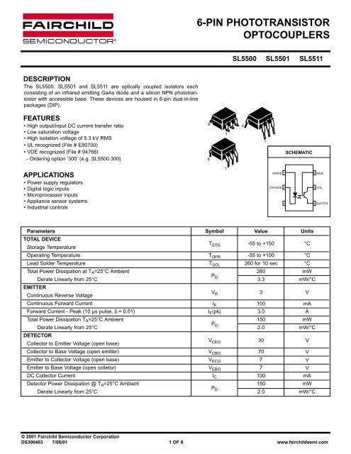
6-<strong>PIN</strong> <strong>PHOTOTRANSISTOR</strong><strong>OPTOCOUPLERS</strong>SL5500 SL5501 SL5511DESCRIPTIONThe SL5500, SL5501 and SL5511 are optically coupled isolators eachconsisting of an infrared emitting GaAs diode and a silicon NPN phototransistorwith accessible base. These devices are housed in 6-pin dual-in-linepackages (DIP).FEATURES• High output/input DC current transfer ratio• Low saturation voltage• High isolation voltage of 5.3 kV RMS• UL recognized (File # E90700)• VDE recognized (File # 94766)- Ordering option ‘300’ (e.g. SL5500.300)66161SCHEMATICAPPLICATIONS• Power supply regulators• Digital logic inputs• Microprocessor inputs• Appliance sensor systems• Industrial controls1ANODE 1CATHODE 236 BASE5 COL4 EMITTERParameters Symbol Value UnitsTOTAL DEVICEStorage TemperatureT STG -55 to +150 °COperating Temperature T OPR -55 to +100 °CLead Solder Temperature T SOL 260 for 10 sec °CTotal Power Dissipation at T A =25°C Ambient260 mWPDerate Linearly from 25°C D3.3 mW/°CEMITTERVContinuous Reverse VoltageR 3 VContinuous Forward Current I F 100 mAForward Current - Peak (10 µs pulse, δ = 0.01) I F (pk) 3.0 ATotal Power Dissipation T A =25°C Ambient150 mWPDerate Linearly from 25°C D2.0 mW/°CDETECTORVCollector to Emitter Voltage (open base)CEO 30 VCollector to Base Voltage (open emitter) V CBO 70 VEmitter to Collector Voltage (open base) V ECO 7 VEmitter to Base Voltage (open colletor) V EBO 7 VDC Collector Current I C 100 mADetector Power Dissipation @ T A =25°C Ambient150 mWPDerate Linearly from 25°C D2.0 mW/°C© 2001 Fairchild Semiconductor CorporationDS300403 7/08/01 1 OF 8 www.fairchildsemi.com
6-<strong>PIN</strong> <strong>PHOTOTRANSISTOR</strong><strong>OPTOCOUPLERS</strong>SL5500 SL5501 SL5511ELECTRICAL CHARACTERISTICS (T A = 25°C Unless otherwise specified.)INDIVIDUAL COMPONENT CHARACTERISTICSParameters Test Conditions Symbol Device Min Typ* Max UnitsEMITTERInput Forward VoltageI F = 20 mA, T A = 25 to 70°C1.23 1.3 VV FAllI F = 2 mA 1.10 1.2 VReverse Current V R = 3 V, T A = 25 to 70°C I R All 0.001 10 µADETECTOR V CE = 10 V 1 50 nALeakage Current Collector to EmitterV CE = 30 V I CEO 0.005 10 µAAllV CE = 10 V, T A = 70°C 500 nAV CB = 30 V I CBO 0.001 50 µABreakdown VoltageCollector to Emitter I C = 10 µA, I F = 0 BV CEO All 30 100 VCollector to Base I C = 10 µA, I F = 0 BV CBO All 30 120 VEmitter to Collector I E = 10 µA, I F = 0 BV ECO All 7 10 VEmitter to Base I E = 10 µA, I F = 0 BV EBO All 7 10 VISOLATION CHARACTERISTICSCharacteristic Test Conditions Symbol Min Typ* Max UnitsInput-Output Isolation Voltage (note 1) f = 60Hz, T = 1 min. V ISO 5300 V AC(RMS)Isolation Resistance V I-O = ±500 VDC R ISO 1 10 T!Isolation Capacitance f = 1 MHz, V = 0V C ISO 0.6 1.3 pF* Typical values at T A =25°C.www.fairchildsemi.com 2 OF 8 7/08/01 DS300403
6-<strong>PIN</strong> <strong>PHOTOTRANSISTOR</strong><strong>OPTOCOUPLERS</strong>SL5500 SL5501 SL5511TRANSFER CHARACTERISTICS (T A = 25°C Unless otherwise specified.)DC Characteristics Test Conditions Symbol Device Min Typ Max UnitsI F = 10 mA, V CE = 0.4 V SL5500 50 300I F = 10 mA, V CE = 0.4 V, T A = 70°C SL5500 40 300I F = 10 mA, V CE = 0. 4 V, T A = 25°C to 70°C SL5501 25 400Output/Input Current Transfer RatioI F = 2 mA, V CE = 5 VSL5500 40CTRI F = 2 mA, V CE = 5 V, T A = 70°C SL5500 30%I F = 2 mA, V CE = 5 V, T A = 25°C to 70°C SL5501 15I F = 2 mA, V CE = 5 V, T A = 25°C to 70°C SL5511 25I F = 0.5 mA, V CE = 0.4 V, T A = 25°C to 70°C SL5511 20Collector-Emitter Saturation VoltageI F = 50 mA, I C = 10 mASL5500 0.4VI CE(SAT)F = 20 mA, I C = 2 mA SL5501, SL5511 0.4VAC Characteristics Test Conditions Symbol Device Min Typ Max UnitsSaturated Switching TimesTurn-On Time R L = 1 kΩ, I F = 16 mA, V CC = 5 V t on All 20 µsTurn-Off Time See Fig. 1 and Fig. 2 t off All 50 µsNote1. Device considered a two-terminal device: pins 1, 2 and 3 shorted together and pins 4, 5 and 6 shorted together.DS300403 7/08/01 3 OF 8 www.fairchildsemi.com
NORMALIZED CTRNORMALIZED CTRV F - FORWARD VOLTAGE (V)NORMALIZED CTR6-<strong>PIN</strong> <strong>PHOTOTRANSISTOR</strong><strong>OPTOCOUPLERS</strong>SL5500 SL5501 SL5511V IV I+V CC0V OV O90%50ΩR L0t ont off10%Fig. 1 Switching CircuitFig. 2 Waveforms1.81.7Fig.3 LED Forward Voltage vs. Forward Current1.41.2Fig.4 Normalized CTR vs. Forward CurrentV CE = 5.0VT A = 25˚CNormalized toI F = 10mA1.61.01.50.81.41.31.21.1T A = - 55 o CT A = 25 o CT A = 100 o C0.60.40.21.01 10 100I F - LED FORWARD CURRENT (mA)0.00 5 10 15 20FORWARD CURRENT - I F (mA)Fig. 5 Normalized CTR vs. Ambient Temperature1.61.0Fig. 7 CTR vs. RBE (Unsaturated)1.41.2I F = 5mA0.90.80.7I F = 20mA1.0I F = 10mA0.60.5I F = 10mA0.8I F = 20mA0.6Normalized toI F = 10 mAT A = 25˚C0.4-75 -50 -25 0 25 50 75 100 125AMBIENT TEMPERATURE - T A ( o C)0.40.30.20.1I F = 5mA0.010 1000R BE - BASE RESISTANCE (kΩ)V CE = 5V, T A = 25˚CNormalized to CTR at RBE = Openwww.fairchildsemi.com 4 OF 8 7/08/01 DS300403
V CEsat - (V)I CEO - COLLECTOR -EMITTER DARK CURRENT (nA)SWITCHING SPEED - (µs)NORMALIZED CTR6-<strong>PIN</strong> <strong>PHOTOTRANSISTOR</strong><strong>OPTOCOUPLERS</strong>SL5500 SL5501 SL5511NORMALIZED t on6.05.55.04.54.03.53.02.52.01.00.90.80.70.60.50.40.3Fig. 7 CTR vs. RBE (Saturated)I F = 20mAI F = 10mAI F = 5mA0.20.1V CE = 0.3V, T A = 25˚CNormalized to CTR at RBE = Open0.010 100 1000Fig. 8 Normalized t off vs. R BE0.110 100 1000 10000R R BE- BASE RESISTANCE (k Ω)BE- BASE RESISTANCE (k Ω)Fig. 9 Normalized ton vs. R BENORMALIZED t off1.41.31.21.11.00.90.80.70.60.50.40.30.2100010010V CC = 10VI C = 2mAR Ω L = 100NORMALIZED TO:t off AT RBE = OPENFig. 10 Switching Speed vs. Load ResistorI F = 10mAV CC = 10VT A = 25 o CT offT f1.5V CC = 10V1.0I C = 2mA0.5R L = 100ΩNORMALIZED TO t on AT RBE = OPEN0.010 100 1000 10000R BE - BASE RESISTANCE (kΩ)Fig. 11 Collector Emitter Saturation Voltage vs. Collector Current100T on1T r0.10.1 1 10 100R-LOAD RESISTOR (k Ω)10100001000Fig. 12 Dark Current vs. Ambient TemperatureV CE = 10VT A = 25 o C1100I F = 2.5mA100.10.01I F = 10mA I F = 20mAI F = 5mA0.10.01T A =25 o C0.0010.0010 20 40 60 80 1000.01 0.1 1 10IT A - AMBIENT TEMPERATURE ( o C)C - (mA)DS300403 7/08/01 5 OF 8 www.fairchildsemi.com
6-<strong>PIN</strong> <strong>PHOTOTRANSISTOR</strong><strong>OPTOCOUPLERS</strong>SL5500 SL5501 SL5511Package Dimensions (Through Hole)Package Dimensions (Surface Mount)<strong>PIN</strong> 1ID.0.350 (8.89)0.330 (8.38)0.270 (6.86)0.240 (6.10)321<strong>PIN</strong> 1ID.0.270 (6.86)0.240 (6.10)SEATING PLANE0.070 (1.78)0.045 (1.14)0.350 (8.89)0.330 (8.38)4560.070 (1.78)0.045 (1.14)0.300 (7.62)TYP0.200 (5.08)0.135 (3.43)0.200 (5.08)0.165 (4.18)0.016 (0.41)0.008 (0.20)0.154 (3.90)0.100 (2.54)0.022 (0.56)0.016 (0.41)0.020 (0.51)MIN0.016 (0.40)0.008 (0.20)0° to 15°0.300 (7.62)TYP0.022 (0.56)0.016 (0.41)0.020 (0.51)MIN0.100 (2.54)TYP0.016 (0.40) MIN0.315 (8.00)MIN0.405 (10.30)MAX0.100 (2.54)TYPLead Coplanarity : 0.004 (0.10) MAXPackage Dimensions (0.4”Lead Spacing)Recommended Pad Layout forSurface Mount Leadform0.270 (6.86)0.240 (6.10)0.070 (1.78)0.060 (1.52)SEATING PLANE0.200 (5.08)0.135 (3.43)0.350 (8.89)0.330 (8.38)0.070 (1.78)0.045 (1.14)0.415 (10.54)0.295 (7.49)0.100 (2.54)0.030 (0.76)0.154 (3.90)0.100 (2.54)0.004 (0.10)MIN0.016 (0.40)0.008 (0.20)0.022 (0.56)0.016 (0.41)0.100 (2.54) TYP0.400 (10.16)TYP0° to 15°NOTEAll dimensions are in inches (millimeters)www.fairchildsemi.com 6 OF 8 7/08/01 DS300403
6-<strong>PIN</strong> <strong>PHOTOTRANSISTOR</strong><strong>OPTOCOUPLERS</strong>SL5500 SL5501 SL5511ORDERING INFORMATIONOption Order Entry Identifier DescriptionS .S Surface Mount Lead BendSD .SD Surface Mount; Tape and reelW .W 0.4” Lead Spacing300 .300 VDE 0884300W .300W VDE 0884, 0.4” Lead Spacing3S .3S VDE 0884, Surface Mount3SD .3SD VDE 0884, Surface Mount, Tape & ReelCarrier Tape Specifications (“D” Taping Orientation)4.85 ± 0.200.30 ± 0.054.0 ± 0.112.0 ± 0.14.0 ± 0.1Ø1.55 ± 0.051.75 ± 0.1013.2 ± 0.27.5 ± 0.116.0 ± 0.39.55 ± 0.200.1 MAX 10.30 ± 0.20Ø1.6 ± 0.1User Direction of FeedNOTEAll dimensions are in inches (millimeters)DS300403 7/08/01 7 OF 8 www.fairchildsemi.com
6-<strong>PIN</strong> <strong>PHOTOTRANSISTOR</strong><strong>OPTOCOUPLERS</strong>SL5500 SL5501 SL5511DISCLAIMERFAIRCHILD SEMICONDUCTOR RESERVES THE THE RIGHT TO MAKE CHANGES WITHOUT FURTHER NOTICETO ANY PRODUCTS HEREIN TO IMPROVE RELIABILITY, FUNCTION OR DESIGN. FAIRCHILD DOES NOTASSUME ANY LIABILITY ARISING OUT OF THE APPLICATION OR USE OF ANY PRODUCT OR CIRCUITDESCRIBED HEREIN; NEITHER DOES IT CONVEY ANY LICENSE UNDER ITS PATENT RIGHTS, NOR THERIGHTS OF OTHERS.LIFE SUPPORT POLICYFAIRCHILD’S PRODUCTS ARE NOT AUTHORIZED FOR USE AS CRITICAL COMPONENTS IN LIFE SUPPORTDEVICES OR SYSTEMS WITHOUT THE EXPRESS WRITTEN APPROVAL OF THE PRESIDENT OF FAIRCHILDSEMICONDUCTOR CORPORATION. As used herein:1. Life support devices or systems are devices orsystems which, (a) are intended for surgicalimplant into the body,or (b) support or sustain life,and (c) whose failure to perform when properlyused in accordance with instructions for use providedin labeling, can be reasonably expected to result in asignificant injury of the user.2. A critical component in any component of a life supportdevice or system whose failure to perform can bereasonably expected to cause the failure of the lifesupport device or system, or to affect its safety oreffectiveness.www.fairchildsemi.com 8 OF 8 7/08/01 DS300403
This datasheet has been download from:www.datasheetcatalog.com<strong>Datasheet</strong>s for electronics components.