Si4020 Universal ISM Band FSK Transmitter
Si4020 Universal ISM Band FSK Transmitter Si4020 Universal ISM Band FSK Transmitter
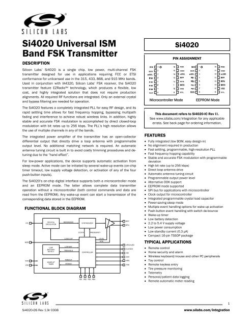
Si4020 Universal ISMBand FSK TransmitterDESCRIPTIONSilicon Labs’ Si4020 is a single chip, low power, multi-channel FSKtransmitter designed for use in applications requiring FCC or ETSIconformance for unlicensed use in the 315, 433, 868, and 915 MHz bands.Used in conjunction with IA4320, Silicon Labs’ FSK receiver, the Si4020transmitter feature EZRadio TM technology, which produces a flexible, lowcost, and highly integrated solution that does not require productionalignments. All required RF functions are integrated. Only an external crystaland bypass filtering are needed for operation.The Si4020 features a completely integrated PLL for easy RF design, and itsrapid settling time allows for fast frequency hopping, bypassing multipathfading and interference to achieve robust wireless links. In addition, highlystable and accurate FSK modulation is accomplished by direct closed-loopmodulation with bit rates up to 256 kbps. The PLL’s high resolution allowsthe use of multiple channels in any of the bands.The integrated power amplifier of the transmitter has an open-collectordifferential output that directly drive a loop antenna with programmableoutput level. No additional matching network is required. An automaticantenna tuning circuit is built in to avoid costly trimming procedures and detuningdue to the “hand effect”.For low-power applications, the device supports automatic activation fromsleep mode. Active mode can be initiated by several wake-up events (on-chiptimer timeout, low supply voltage detection, or activation of any of the fourpush-button inputs).The Si4020’s on-chip digital interface supports both a microcontroller modeand an EEPROM mode. The latter allows complete data transmitteroperation without a microcontroller (both control commands and data areread from the EEPROM). Any wake-up event can start a transmission of thecorresponding data stored in the EEPROM.FUNCTIONAL BLOCK DIAGRAMXTLMODVDDVSSCRYSTALOSCILLATORLOWBATTERYDETECTWAKE-UPTIMERREFERENCELOAD CAPLOW BATTRESHOLDTIMEOUTPERIODCLOCKPB1SYNTHESIZERCONTROLLERPB2PB3FREQUENCYPB4LEVELOOKRFPRFNnIRQ/nLBDCLK/SDOSDISCKnSELFSKMicrocontroller ModeSi4020PIN ASSIGNMENTEEPROM ModeThis document refers to Si4020-IC Rev I1.See www.silabs.com/integration for any applicableerrata. See back page for ordering information.FEATURES• Fully integrated (low BOM, easy design-in)• No alignment required in production• Fast settling, programmable, high-resolution PLL• Fast frequency hopping capability• Stable and accurate FSK modulation with programmabledeviation• High bit rate (up to 256 kbps)• Direct loop antenna drive• Automatic antenna tuning circuit• Programmable output power level• Alternative OOK support• EEPROM mode supported• SPI bus for applications with microcontroller• Clock output for microcontroller• Integrated programmable crystal load capacitor• Power-saving sleep mode• Multiple event handling options for wake-up activation• Push-button event handling with switch de-bounce• Wake-up timer• Low battery detection• 2.2 to 5.4 V supply voltage• Low power consumption• Low standby current (0.3 µA)• Compact 16-pin TSSOP packageTYPICAL APPLICATIONS• Remote control• Home security and alarm• Wireless keyboard/mouse and other PC peripherals• Toy control• Remote keyless entry• Tire pressure monitoring• Telemetry• Personal/patient data logging• Remote automatic meter readingSi4020-DS Rev 1.9r 03081www.silabs.com/integration
- Page 2 and 3: Si4020DETAILED DESCRIPTIONThe Si402
- Page 4 and 5: Si4020Typical Application, Microcon
- Page 6 and 7: Si4020Typical Application, EEPROM M
- Page 8 and 9: Si4020AC CharacteristicsSymbol Para
- Page 10 and 11: Si4020TYPICAL PERFORMANCE DATAUnmod
- Page 12 and 13: Si4020CONTROL INTERFACECommands to
- Page 14 and 15: Si40202. Power Management Commandbi
- Page 16 and 17: Si40206. Low Battery Detector Comma
- Page 18 and 19: Si40209. Wake-Up Timer Commandbit 1
- Page 20 and 21: Si402011. Status Register Read Comm
- Page 22 and 23: Si4020Push-button 1:00000080 88 72
- Page 24 and 25: RESET MODESSi4020The chip will ente
- Page 26 and 27: Si4020SIMPLIFIED INTERNAL CONTROL A
- Page 28 and 29: Si4020EXAMPLE APPLICATIONSFor Micro
- Page 30 and 31: Si4020PACKAGE INFORMATION16-pin TSS
- Page 32: Si4020RELATED PRODUCTS AND DOCUMENT
<strong>Si4020</strong> <strong>Universal</strong> <strong>ISM</strong><strong>Band</strong> <strong>FSK</strong> <strong>Transmitter</strong>DESCRIPTIONSilicon Labs’ <strong>Si4020</strong> is a single chip, low power, multi-channel <strong>FSK</strong>transmitter designed for use in applications requiring FCC or ETSIconformance for unlicensed use in the 315, 433, 868, and 915 MHz bands.Used in conjunction with IA4320, Silicon Labs’ <strong>FSK</strong> receiver, the <strong>Si4020</strong>transmitter feature EZRadio TM technology, which produces a flexible, lowcost, and highly integrated solution that does not require productionalignments. All required RF functions are integrated. Only an external crystaland bypass filtering are needed for operation.The <strong>Si4020</strong> features a completely integrated PLL for easy RF design, and itsrapid settling time allows for fast frequency hopping, bypassing multipathfading and interference to achieve robust wireless links. In addition, highlystable and accurate <strong>FSK</strong> modulation is accomplished by direct closed-loopmodulation with bit rates up to 256 kbps. The PLL’s high resolution allowsthe use of multiple channels in any of the bands.The integrated power amplifier of the transmitter has an open-collectordifferential output that directly drive a loop antenna with programmableoutput level. No additional matching network is required. An automaticantenna tuning circuit is built in to avoid costly trimming procedures and detuningdue to the “hand effect”.For low-power applications, the device supports automatic activation fromsleep mode. Active mode can be initiated by several wake-up events (on-chiptimer timeout, low supply voltage detection, or activation of any of the fourpush-button inputs).The <strong>Si4020</strong>’s on-chip digital interface supports both a microcontroller modeand an EEPROM mode. The latter allows complete data transmitteroperation without a microcontroller (both control commands and data areread from the EEPROM). Any wake-up event can start a transmission of thecorresponding data stored in the EEPROM.FUNCTIONAL BLOCK DIAGRAMXTLMODVDDVSSCRYSTALOSCILLATORLOWBATTERYDETECTWAKE-UPTIMERREFERENCELOAD CAPLOW BATTRESHOLDTIMEOUTPERIODCLOCKPB1SYNTHESIZERCONTROLLERPB2PB3FREQUENCYPB4LEVELOOKRFPRFNnIRQ/nLBDCLK/SDOSDISCKnSEL<strong>FSK</strong>Microcontroller Mode<strong>Si4020</strong>PIN ASSIGNMENTEEPROM ModeThis document refers to <strong>Si4020</strong>-IC Rev I1.See www.silabs.com/integration for any applicableerrata. See back page for ordering information.FEATURES• Fully integrated (low BOM, easy design-in)• No alignment required in production• Fast settling, programmable, high-resolution PLL• Fast frequency hopping capability• Stable and accurate <strong>FSK</strong> modulation with programmabledeviation• High bit rate (up to 256 kbps)• Direct loop antenna drive• Automatic antenna tuning circuit• Programmable output power level• Alternative OOK support• EEPROM mode supported• SPI bus for applications with microcontroller• Clock output for microcontroller• Integrated programmable crystal load capacitor• Power-saving sleep mode• Multiple event handling options for wake-up activation• Push-button event handling with switch de-bounce• Wake-up timer• Low battery detection• 2.2 to 5.4 V supply voltage• Low power consumption• Low standby current (0.3 µA)• Compact 16-pin TSSOP packageTYPICAL APPLICATIONS• Remote control• Home security and alarm• Wireless keyboard/mouse and other PC peripherals• Toy control• Remote keyless entry• Tire pressure monitoring• Telemetry• Personal/patient data logging• Remote automatic meter reading<strong>Si4020</strong>-DS Rev 1.9r 03081www.silabs.com/integration
<strong>Si4020</strong>DETAILED DESCRIPTIONThe <strong>Si4020</strong> <strong>FSK</strong> transmitter is designed to cover the unlicensedfrequency bands at 315, 433, 868, and 915 MHz. The devicefacilitates compliance with FCC and ETSI requirements.PLLThe programmable PLL synthesizer determines the operatingfrequency, while preserving accuracy based on the on-chipcrystal-controlled reference oscillator. The PLL’s high resolutionallows the usage of multiple channels in any of the bands. The<strong>FSK</strong> deviation is selectable (from 30 to 240 kHz with 30 kHzincrements) to accommodate various bandwidth, data rate andcrystal tolerance requirements, and it is also highly accurate dueto the direct closed-loop modulation of the PLL. The transmitteddigital data can be sent asynchronously through the <strong>FSK</strong> pin orover the control interface using the appropriate command.The RF VCO in the PLL performs automatic calibration, whichrequires only a few microseconds. To ensure proper operation inthe programmed frequency band, the RF VCO is automaticallycalibrated upon activation of the synthesizer. If temperature orsupply voltage change significantly or operational band haschanged, VCO recalibration is recommended.. Recalibration canbe initiated at any time by switching the synthesizer off and backon again.RF Power Amplifier (PA)The power amplifier has an open-collector differential output andcan directly drive a loop antenna with a programmable outputpower level. An automatic antenna tuning circuit is built in toavoid costly trimming procedures and the so-called “hand effect.”The transmitters can operate in On-Off Keying (OOK) mode byswitching the power amplifier on and off. When the appropriatecontrol bit is set using the Power Setting Command, the <strong>FSK</strong> pinbecomes an enable input (active high) for the power amplifier.Crystal OscillatorThe chip has a single-pin crystal oscillator circuit, which providesa 10 MHz reference signal for the PLL. To reduce external partsand simplify design, the crystal load capacitor is internal andprogrammable. Guidelines for selecting the appropriate crystalcan be found later in this datasheet.The transmitters can supply the clock signal for themicrocontroller, so accurate timing is possible without the needfor a second crystal. When the chip receives a Sleep Commandfrom the microcontroller and turns itself off, it provides severalfurther clock pulses (“clock tail”) for the microcontroller to beable to go to idle or sleep mode. The length of the clock tail isprogrammable.Low Battery Voltage DetectorThe low battery voltage detector circuit monitors the supplyvoltage and generates an interrupt if it falls below aprogrammable threshold level. The detector circuit has 50 mVhysteresis.Wake-Up TimerThe wake-up timer has very low current consumption (1.5 uAtypical) and can be programmed from 1 ms to several days withan accuracy of ±5%.It calibrates itself to the crystal oscillator at every startup. Whenthe oscillator is switched off, the calibration circuit switches onthe crystal oscillator only long enough for a quick calibration (afew milliseconds) to facilitate accurate wake-up timing.Event HandlingIn order to minimize current consumption, the device supportssleep mode. Active mode can be initiated by several wake-upevents: timeout of wake-up timer, detection of low supplyvoltage, pressing any of the four push-button inputs, or throughthe serial interface. The push-button inputs can be driven by alogic signal from a microcontroller or controlled directly bynormally open switches. Pull-up resistors are integrated.If any wake-up event occurs, the wake-up logic generates aninterrupt, which can be used to wake up the microcontroller,effectively reducing the period the microcontroller has to beactive. The cause of the interrupt can be read out from thetransmitters by the microcontroller through the nIRQ pin.InterfaceAn SPI compatible serial interface lets the user select theoperating frequency band and center frequency of thesynthesizer, polarity and deviation of <strong>FSK</strong> modulation, and outputpower level. Division ratio for the microcontroller clock, wake-uptimer period, and low battery detector threshold are alsoprogrammable. Any of these auxiliary functions can be disabledwhen not needed. All parameters are set to default after poweron;the programmed values are retained during sleep mode.EEPROM ModeIn simple applications, the on-chip digital controller provides thetransmitters with direct interface to a serial (SPI) EEPROM. In thiscase, no external microcontroller is necessary. Wake-up eventsinitiate automatic readout of the assigned command sequencefrom EEPROM memory. For every event, there is a dedicatedstarting address available in the EEPROM.Programming the EEPROM is very simple. Any control commandcan be programmed in the EEPROM sequentially (same as inmicrocontroller mode).The internal power-on reset (POR) is a dedicated event, whichcan be used to program the basic settings of the transmitters. Inthis case the chip starts to read out the preprogrammed datafrom the 00h address in EEPROM. Data can be transmitted withthe help of the Data Transmit Command, which tells thetransmitters how many bytes must be transmitted. The wholeprocess finishes with a Sleep Command.2
<strong>Si4020</strong>PACKAGE PIN DEFINITIONS, MICROCONTROLLER MODEPin type key: D=digital, A=analog, S=supply, I=input, O=output, IO=input/outputMicrocontroller Mode Pin AssignmentPin Name Type Function1 SDI DI Data input of serial control interface2 SCK DI Clock input of serial control interface3 nSEL DI Chip select input of serial control interface (active low)4 PB1 DI Push-button input #1 (active low with internal pull-up resistor)5 PB2 DI Push-button input #2 (active low with internal pull-up resistor)6 PB3 DI Push-button input #3 (active low with internal pull-up resistor)7 PB4 DI Push-button input #4 (active low with internal pull-up resistor)8 CLK DO Microcontroller clock (1 MHz-10 MHz)9 XTL AIO Crystal connection (other terminal of crystal to VSS)10 VSS S Ground reference11 MOD DI Connect to logic high (microcontroller mode)12 RFN AO Power amplifier output (open collector)13 RFP AO Power amplifier output (open collector)14 nIRQ DO Interrupt request output for microcontroller (active low) and status read output15 VDD S Positive supply voltage16 <strong>FSK</strong> DI Serial data input for <strong>FSK</strong> modulation3
<strong>Si4020</strong>Typical Application, Microcontroller ModeVDDC12.2µFC210nFC3GNDD1LEDREDR1470GP6To other GP7circuits GP8GP9GNDMICROCONTROLLERGP5GP3GP4GP2GP1GP0CLKin(EC osc. mode)OPTIONALSDISCKnSELPB1PB2PB3PB4CLK1 162 153 144 135 IA4220 126 117 108 9<strong>FSK</strong>VDDnIRQRFPRFNMODVSSXTLAntennaX110MHzS1S2S3S4GNDGNDOPTIONALGNDNote: For detailed information about the supply decoupling capacitors see page 6.4
<strong>Si4020</strong>PACKAGE PIN DEFINITIONS, EEPROM MODEPin type key: D=digital, A=analog, S=supply, I=input, O=output, IO=input/outputEEPROM Mode Pin AssignmentPin Name Type Function1 SDI DI Data input of serial control interface2 SCK DO Clock output of serial control interface3 nSEL DO Chip select output of serial control interface (active low)4 PB1 DI Push-button input #1 (active low with internal pull-up resistor)5 PB2 DI Push-button input #2 (active low with internal pull-up resistor)6 PB3 DI Push-button input #3 (active low with internal pull-up resistor)7 PB4 DI Push-button input #4 (active low with internal pull-up resistor)8 SDO DO Data output of serial control interface9 XTL AIO Crystal connection (other terminal of crystal to VSS)10 VSS S Ground reference11 MOD DI Connect to logic low (EEPROM mode)12 RFN AO Power amplifier output (open collector)13 RFP AO Power amplifier output (open collector)14 nLBD DO Low battery voltage detector output (active low)15 VDD S Positive supply voltage16 <strong>FSK</strong> DI Not used, connect to VDD or VSS5
<strong>Si4020</strong>Typical Application, EEPROM ModeVDDC12.2µFC210nFC3R1470GNDnCSSOnWPGND1 827EEPROM3625AA0804 5VCCHOLDSCKSID1LEDREDGNDOPTIONALSDISCKnSELPB1PB2PB3PB4SD01 162 153 144 135 IA4220 126 117 108 9X110MHz<strong>FSK</strong>VDDnLBDxRFPRFNMODVSSXTLAntennaS1S2S3S4GNDGNDGNDRecommended supply decoupling capacitor valuesC2 and C3 should be 0603 size ceramic capacitors to achieve the best supply decoupling. The capacitor values are valid for bothstand-alone and microcontroller mode.<strong>Band</strong> [MHz] C1 C2 C3315 2.2µF 10nF 390pF433 2.2µF 10nF 220pF868 2.2µF 10nF 47pF915 2.2µF 10nF 33pF6
<strong>Si4020</strong>GENERAL DEVICE SPECIFICATIONSAll voltages are referenced to Vss, the potential on the ground reference pin VSS.Absolute Maximum Ratings (non-operating)Symbol Parameter Min Max UnitsV dd Positive supply voltage -0.5 6.0 VV in Voltage on any pin except open collector outputs -0.5 V dd +0.5 VV oc Voltage on open collector outputs -0.5 6.0 VI in Input current into any pin except VDD and VSS -25 25 mAESD Electrostatic discharge with human body model 1000 VT st Storage temperature -55 125 ºCT ld Lead temperature (soldering, max 10 s) 260 ºCRecommended Operating RangeSymbol Parameter Min Max UnitsV dd Positive supply voltage 2.2 5.4 VV oc Voltage on open collector outputs (Max 6.0 V) V dd - 1 V dd + 1 VT op Ambient operating temperature -40 85 ºCELECTRICAL SPECIFICATION(Min/max values are valid over the whole recommended operating range, typical conditions: Top = 27 o C; Vdd = Voc = 2.7 V)DC CharacteristicsSymbol Parameter Conditions/Notes Min Typ Max UnitsI dd_TX_0I dd_TX_PMAXSupply current(TX mode, P out = 0 dBm)Supply current(TX mode, P out = P max )315 MHz band 9433 MHz band 10868 MHz band 12915 MHz band 13315 MHz band 11433 MHz band 12868 MHz band 14915 MHz band 15I pd Standby current in sleep mode All blocks disabled (Note 1) 0.3 µAI w t Wake-up timer current consumption 1.5 µAI lbLow battery detector currentconsumptionmAmA0.5 µAI x Idle current Only crystal oscillator is on 1.5 mAV lba Low battery detection accuracy 75 mVV lb Low battery detector threshold Programmable in 0.1 V steps 2.2 5.3 VV il Digital input low level 0.3*V dd VV ih Digital input high level 0.7*V dd VI il Digital input current V il = 0 V -1 1 µAI ih Digital input current V ih = V dd , V dd = 5.4 V -1 1 µAV ol Digital output low level I ol = 2 mA 0.4 VV oh Digital output high level I oh = -2 mA V dd -0.4 VNote for table above is on page 7.7
<strong>Si4020</strong>AC CharacteristicsSymbol Parameter Conditions/Notes Min Typ Max Unitsf ref PLL reference frequency Crystal operation mode is parallel (Note 2) 8 10 12 MHzf ot lockOutput frequency (programmable)PLL lock time315 MHz band, 2.5 kHz resolution 310.24 319.75433 MHz band, 2.5 kHz resolution 430.24 439.75868 MHz band, 5.0 kHz resolution 860.48 879.51915 MHz band, 7.5 kHz resolution 900.72 929.27Frequency error < 10 kHz after 10 MHzstepMHz20 µst spPLL startup timeAfter turning on from idle mode, withcrystal oscillator already stable250 µsI OUT Open collector output current (Note 3) At all bands 0.1 2.5 mAP maxLP maxHAvailable output power(315 and 433 MHz band)Available output power(868 and 915 MHz band)With optimal antenna impedance(Note 4)With optimal antenna impedance(Note 4)3 dBm1 dBmP out Typical output power Selectable in 3 dB steps (Note3) P max -21 P max dBmP spC oQ oL outSpurious emissionAt max power with loop antenna(Note 5)Output capacitance (set by the At low bands 1.5 2.3 3.1automatic antenna tuning circuit) At high bands 1.6 2.2 2.8Quality factor of the outputcapacitanceOutput phase noise16 18 22100 kHz from carrier -751 MHz from carrier -85-50 dBcBR <strong>FSK</strong> <strong>FSK</strong> bit rate 256 kbpsBR OOK OOK bit rate 512 kbpsdf fsk <strong>FSK</strong> frequency deviation Programmable in 30 kHz steps 30 240 kHzC xlt PORCrystal load capacitanceSee Crystal Selection GuidelinesInternal POR timeout(Note 6)Programmable in 0.5 pF steps, tolerance+/- 10%pFdBc/Hz8.5 16 pFAfter V dd has reached 90% of final value 100 mst sx Crystal oscillator startup time Crystal ESR < 100 Ohms (Note 7) 1 5 mst PBtWake-up timer clock accuracyCrystal oscillator must be enabled toensure proper calibration at startup(Note 7)+/-10% mst wake-up Programmable wake-up time 1 2 · 10 9 msC in, D Digital input capacitance 2 pFt r, f Digital output rise/fall time 15 pF pure capacitive load 10 nsAll notes for table above are on page 7.8
<strong>Si4020</strong>Note 1:Note 2:Note 3:Note 4:Using a CR2032 battery (225 mAh capacity), the expected battery life is greater than 2 years using a 60-second wake-up periodfor sending 100 byte packets in length at 19.2 kbps with +3 dBm output power in the 915 MHz band.Using anything but a 10 MHz crystal is allowed but not recommended because all crystal-referred timing and frequencyparameters will change accordingly.Adjustable in 8 steps.Optimal antenna admittance/impedance for the <strong>Si4020</strong>:Yantenna [S] Zantenna [Ohm] Lantenna [nH]315 MHz 9.4E-4 - j4.5E-3 43 + j214 112.00434 MHz 8.4E-4 - j6.25E-3 21 + j157 59.00868 MHz 1.15E-3 - j1.2E-2 7.9 + j83 15.30915 MHz 1.2E-3 - j1.25E-2 7.6 + j79 13.90Note 5:Note 6:Note 7:With selective resonant antennas (see: Application Notes available from http://www.silabs.com/integration).During this period, no commands are accepted by the chip. For detailed information see the Reset modes section.The crystal oscillator start-up time strongly depends on the capacitance seen by the oscillator. Using low capacitance and low ESRcrystal is recommended. When designing the PCB layout keep the trace connecting to the crystal short to minimize straycapacitance.9
<strong>Si4020</strong>TYPICAL PERFORMANCE DATAUnmodulated RF SpectrumThe output spectrum is measured at different frequencies. The output is loaded with 50 Ohms through a matching network.At 315 MHzAt 433 MHz15:37:47 Dec 15, 200315:18:59 Oct 29, 2003Ref -10 dBmSampLog10dB/Atten 5 dB1Mkr1 315.0010 MHz-22.7 dBmRef -10 dBmSampLog10dB/#Atten 5 dB1Mkr1 434.0630 MHz-23.41 dBmVAvg100W1 S2S3 FCAAVAvg100W1 S2S3 FCAACenter 315 MHzRes BW 10 kHzVBW 10 kHzSpan 2 MHzSweep 40.74 ms (2001 pts)Center 434.1 MHzRes BW 10 kHzVBW 10 kHzSpan 2 MHzSweep 40.74 ms (2001 pts)At 868 MHzAt 915 MHzRef -10 dBmSampLog10dB/15:20:49 Oct 29, 2003#Atten 5 dB1Mkr1 868.0680 MHz-23.23 dBmRef -10 dBmSampLog10dB/15:28:02 Dec 15, 2003Atten 5 dB1Mkr1 915.0000 MHz-24.63 dBmVAvg100W1 S2S3 FCAAVAvg100W1 S2S3 FCAACenter 868.1 MHzRes BW 10 kHzVBW 10 kHzSpan 2 MHzSwee p 40.74 ms (2001 pts)Center 915 MHzRes BW 10 kHzVBW 10 kHzSpan 2 MHzSweep 40.74 ms (2001 pts)10
<strong>Si4020</strong>Modulated RF SpectrumAt 433 MHz with180 kHz Deviation at 64 kbpsAt 868 MHz with180 kHz Deviation at 64 kbps15:46:09 Oct 29, 200315:43:45 Oct 29, 2003Ref -10 dBm#PeakLog10dB/Atten 5 dBRef -10 dBm#PeakLog10dB/Atten 5 dBVAvg100W1S2S3 FCAAVAvg100W1S2S3 FCAACenter 434 MHzRes BW 10 kHzVBW 100 kHzSpan 2 MHzSweep 20.07 ms (2001 pts)Center 868 MHzRes BW 10 kHzVBW 100 kHzSpan 2 MHzSweep 20.07 ms (2001 pts)Spurious RF SpectrumWith 10 MHz CLK Output Enabled at 433 MHzpRef 0 dBm#PeakLog10dB/16:29:03 Jun 17, 2003Atten 10 dB1RMkr1 ∆ 20.0 MHz-55.11 dBRef -36 dBmPeakLog1dB/Antenna Tuning Characteristics750–970 MHz16:54:54 Mar 11, 2003#Atten 0 dB1Mkr1 915.0 MHz-37.62 dBm*Marker ∆20.000000 MHz-55.11 dBMarker915.000000 MHz-37.62 dBmW1S2S3 FCAA1V1 M2S3 FCAACenter 434.8 MHz#Res BW 3 kHz#VBW 300 HzSpan 50 MHzSweep 45.47 s (401 pts)Start 700 MHz#Res BW 1 MHzVBW 1 MHzStop 1.05 GHzSweep 50 ms (401 pts)The antenna tuning characteristics was recorded in “max-hold” state of the spectrum analyzer. During the measurement, thetransmitters were forced to change frequencies by forcing an external reference signal to the XTL pin. While the carrier was changingthe antenna tuning circuit switched trough all the available states of the tuning circuit. The graph clearly demonstrates that while thecomplete output circuit had about a 40 MHz bandwidth, the tuning allows operating in a 220 MHz band. In other words the tuningcircuit can compensate for 25% variation in the resonant frequency due to any process or manufacturing spread.11
<strong>Si4020</strong>CONTROL INTERFACECommands to the transmitters are sent serially. Data bits on pin SDI are shifted into the device upon the rising edge of the clock onpin SCK whenever the chip select pin nSEL is low. When the nSEL signal is high, it initializes the serial interface. The number of bitssent is an integer multiple of 8. All commands consist of a command code, followed by a varying number of parameter or data bits.All data are sent MSB first (e.g. bit 15 for a 16-bit command). Bits having no influence (don’t care) are indicated with X. The PowerOn Reset (POR) circuit sets default values in all control and command registers.Timing SpecificationSymbol Parameter Minimum value [ns]t CH Clock high time 25t CL Clock low time 25t SS Select setup time (nSEL falling edge to SCK rising edge) 10t SH Select hold time (SCK falling edge to nSEL rising edge) 10t SHI Select high time 25t DS Data setup time (SDI transition to SCK rising edge) 5t DH Data hold time (SCK rising edge to SDI transition) 5t OD Data delay time 10t BL Push-button input low time 25Timing Diagramt SSt SHInSELt CHt CLSCKt DSt DHSDIBIT15 BIT14 BIT13BIT8t ODWK-UP nIRQt SHBIT7BIT1BIT0nIRQPOR12
<strong>Si4020</strong>Control CommandsControl Command1 Configuration Setting Command2 Power Management CommandRelated Parameters/FunctionsFrequency band, microcontroller clock output, crystal load capacitance, frequencydeviationCrystal oscillator, synthesizer, power amplifier, low battery detector, wake-up timer, clockoutput buffer3 Frequency Setting Command Carrier frequency4 Data Rate Command Bit rate (at EEPROM mode only)5 Power Setting Command Nominal output power, OOK mode6 Low Battery Detector Command Low battery threshold limit7 Sleep Command Length of the clock tail after power down8 Push-Button Command Push-button related functions9 Wake-Up Timer Command Wake-up time period10 Data Transmit Command Data transmission11 Status Register Command <strong>Transmitter</strong> status readNote: In the following tables the POR column shows the default values of the command registers after power-on.1. Configuration Setting Commandbit 15 14 13 12 11 10 9 8 7 6 5 4 3 2 1 0 POR1 0 0 b1 b0 d2 d1 d0 x3 x2 x1 x0 ms m2 m1 m0 8080hb1 b0 Frequency <strong>Band</strong> [MHz]0 0 3150 1 4331 0 8681 1 915d2 d1 d0Clock Output Frequency[MHz]0 0 0 10 0 1 1.250 1 0 1.660 1 1 21 0 0 2.51 0 1 3.331 1 0 51 1 1 10x3 x2 x1 x0 Crystal Load Capacitance [pF]0 0 0 0 8.50 0 0 1 9.00 0 1 0 9.50 0 1 1 10.0…1 1 1 0 15.51 1 1 1 16.0The resulting output frequency can be calculated as:f out= f 0– (-1) SIGN * (M + 1) * (30 kHz)where:f 0is the channel center frequency (see the next command)M is the three bit binary number SIGN = (ms) XOR (<strong>FSK</strong> input)13
<strong>Si4020</strong>2. Power Management Commandbit 15 14 13 12 11 10 9 8 7 6 5 4 3 2 1 0 POR1 1 0 0 0 0 0 0 a1 a0 ex es ea eb et dc C000hBits 5-0, enable the corresponding block of the transmitters, i.e. the crystal oscillator is enabled by the ex bit, the synthesizer by es, thepower amplifier by ea and the low battery detector by eb, while the wake-up timer by et. The bit dc disables the clock output buffer.When receiving the Data Transmit Command, the chip supports automatic on/off control over the crystal oscillator, the PLL and the PA.If bit a1 is set, the crystal oscillator and the synthesizer are controlled automatically. Data Transmit Command starts up the crystal oscillatorand as soon as a stable reference frequency is available the synthesizer starts. After a subsequent delay to allow locking of the PLL, if a0 isset the power amplifier is turned on as well.Note:• To enable the automatic internal control of the crystal oscillator, the synthesizer and the power amplifier, the corresponding bits(ex, es, ea) must be zero in the Power Management Command.• In microcontroller mode, the ex bit should be set in the Power Management Command for the correct control of es and ea. Theoscillator can be switched off by clearing the ex bit after the transmission.• In EEPROM operation mode after an identified Data Transmit Command the internal logic switches on the synthesizer and PA. Atthe end of Data Transmit Command header if necessary the current clock cycle is automatically extended to ensure the PLLstabilization and RF power ramp-up.• In EEPROM operation mode the internal logic switches off the PA when the given number of bytes is transmitted. (See: DataTransmit Command in EEPROM operation.)• When the chip is controlled by a microcontroller, the Sleep Command can be used to indicate the end of the data transmissionprocess, because in microcontroller mode the Data Transmit Command does not contain the length of the TX data.• For processing the events caused by the peripheral blocks (POR, LBD, wake-up timer, push-buttons) the chip requires operation ofthe crystal oscillator. This operation is fully controlled internally, independently from the status of the ex bit, but if the dc bit is zero,the oscillator remains active until Sleep Command is issued. (This command can be considered as an event controller reset.)Oscillator control logic14
<strong>Si4020</strong>3. Frequency Setting Commandbit 15 14 13 12 11 10 9 8 7 6 5 4 3 2 1 0 POR1 0 1 0 f11 f10 f9 f8 f7 f6 f5 f4 f3 f2 f1 f0 A7D0hThe 12-bit parameter of the Frequency Setting Command has the value F. The value F should be in the rangeof 96 and 3903. When F is out of range, the previous value iskept. The synthesizer center frequency f 0can be calculated as:f 0= 10 MHz * C1 * (C2 + F/4000)The constants C1 and C2 are determined bythe selected band as:<strong>Band</strong> [MHz] C1 C2315 1 31433 1 43868 2 43915 3 30Note:• For correct operation of the frequency synthesizer, the frequency and band of operation need to be programmed before thesynthesizer is started. Directly after activation of the synthesizer, the RF VCO is calibrated to ensure proper operation in theprogrammed frequency band.• When coding for the <strong>Si4020</strong>, it is suggested that recalibration routines be added to compensate for significant changes intemperature and supply voltages.4. Data Rate Commandbit 15 14 13 12 11 10 9 8 7 6 5 4 3 2 1 0 POR1 1 0 0 1 0 0 0 r7 r6 r5 r4 r3 r2 r1 r0 C800hIn EEPROM mode the transmitted bit rate is determined by the 8-bit value R (bits ) as:BR = 10 MHz / 29 / (R+1)Apart from setting custom values, the standard bit rates from 2.4 to 115.2 kbps can be approximated with minimal error.The commands are read out with a different fixed bit rate:Fsck = 10 MHz / 29 / 3 [~115.2 kHz]5. Power Setting Commandbit 7 6 5 4 3 2 1 0 POR1 0 1 1 ook p2 p1 p0 B0hThe bit ook enables the OOK mode for the PA, in this case the data to be transmitted are received through the <strong>FSK</strong> pin.p2 p1 p0 Relative Output Power [dB]0 0 0 00 0 1 -30 1 0 -60 1 1 -91 0 0 -121 0 1 -151 1 0 -181 1 1 -21The output power is given in the table as relative to themaximum available power, which depends on the actualantenna impedance. (See: Antenna Application Noteavailable from www.silabs.com/integration).15
<strong>Si4020</strong>6. Low Battery Detector Commandbit 15 14 13 12 11 10 9 8 7 6 5 4 3 2 1 0 POR1 1 0 0 0 0 1 0 0 0 0 t4 t3 t2 t1 t0 C200hThe 5-bit value T of determines the threshold voltage Vlb of the detector:V lb= 2.25 V + T * 0.1 V7. Sleep Commandbit 15 14 13 12 11 10 9 8 7 6 5 4 3 2 1 0 POR1 1 0 0 0 1 0 0 s7 s6 s5 s4 s3 s2 s1 s0 C400hThe effect of this command depends on the Power Management Command. It immediately disables the power amplifier (if a0=1 andea=0) and the synthesizer (if a1=1 and es=0). Stops the crystal oscillator after S periods of the microcontroller clock (if a1=1 andex=0) to enable the microcontroller to execute all necessary commands before entering sleep mode itself. The 8-bit value S isdetermined by bits .8. Push-Button Commandbit 15 14 13 12 11 10 9 8 7 6 5 4 3 2 1 0 POR1 1 0 0 1 0 1 0 p4 d1 d0 b4 b3 b2 b1 bc CA00hIf the corresponding bit was set (b1-b4) the event remains active while the button is pressed. In EEPROM mode, the chip is continuouslyperforming the routine assigned to the push-button while it is pressed. In microcontroller mode, the chip continuously generates interruptson nIRQ until the push-button is released. Weak pull-up currents are switched off when bc is high.The d0, d1 bits set the de-bouncing time period:d1 d0 De-bouncing Time [ms]0 0 1600 1 401 0 101 1 0 (Bypassed)Note:• Until the de-bouncing time has expired, the crystal oscillator remains switched on, independent of the status of the ex bit in thePower Management Command. (Because the circuit uses the crystal oscillator signal for timing.)If the p4 bit is set, the controller performs the routine assigned to the fourth button when PB1 and PB2 are pressed downsimultaneously. With the addition of this feature, there is a way to build a device that uses 3 buttons, but performs 4 functions.It is possible to detect multiple pressed push-buttons in both modes. In EEPROM mode the controller executes sequentially all theroutines belonging to the pressed buttons.16
<strong>Si4020</strong>Simultaneously Pressed Push-Button Detect by MicrocontrollerMicrocontroller modeVddPOR(internal)Push buttoninput 1Push buttoninput 2nIRQPOR PB1 PB1 PB2 PB1 PB2 PB1PB_nIRQdly*SPIStatus rdStatus rd Status rd Status rd Status rd Status rd Status rdNote:*PB_nIRQdly is equal with thedebounce timeSimplified Block Diagram of Push-Button 1–4 InputsVDDVDDPOR, LBD, WAKE UP TIMER,P. BUTTONS EVENT FLAGSNotice:Only one EVENT isserviced simultaneouslythe others are pending.WEAK PULL-UPENABLE/DISABLEbcDQEVENT FLAGPush-button1,2,3CLKDigital glitchfilterCLRCLR for P.B1,2SLEEP Command *STAT. REG. READ Command **Internalblocker signaltoPush-button1andPush-button2COUNT/SINGLEb1, b2, b3p4Push-button4Push-button1Push-button2With internal weak pull-upTo Digital glitch filter forPush-button4Note:* In EEprom mode** In uC controlled mode17
<strong>Si4020</strong>9. Wake-Up Timer Commandbit 15 14 13 12 11 10 9 8 7 6 5 4 3 2 1 0 POR1 1 1 r4 r3 r2 r1 r0 m7 m6 m5 m4 m3 m2 m1 m0 E000hThe wake-up time period can be calculated as:Twake-up = M * 2R [ms] ,where M is defined by the digital value and R is defined by the digital value.The value of R should be in the range of 0 and 23. The maximum achievable wake-up time period can be up to 24 days.Note:• For continual operation the et bit should be cleared and set at the end of every cycle.Software reset: Sending FF00h command to the chip triggers software reset. For more details see the Reset modes section.10. Data Transmit CommandThis command is not needed if the transmitters’ power management bits (ex, es, ea) are fully controlled by the microcontroller andTX data comes through the <strong>FSK</strong> pin.In EEPROM operation mode:bit 15 14 13 12 11 10 9 8 7 6 5 4 3 2 1 0 POR1 1 0 0 0 1 1 0 n7 n6 n5 n4 n3 n2 n1 n0 - -In microcontroller slave mode:bit 7 6 5 4 3 2 1 0 POR1 1 0 0 0 1 1 0 - -This command indicates that the following bitstream coming in via the serial interface is to be transmitted. In EEPROM mode, the 8-bit value N of bits contains the number of data bytes to follow.Note:• If the crystal oscillator was formerly switched off (ex=0), the internal oscillator needs t sxtime, to switch on. The actual valuedepends on the type of quartz crystal used.• If the synthesizer was formerly switched off (es=0), the internal PLL needs t spstartup time. Valid data can be transmitted only whenthe internal locking process is finished.• In EEPROM mode, before issuing the Data Transmit Command, the power amplifier must be enabled, with the ea or a0 bit in thePower Management Command.• In EEPROM mode, when N bytes have been read and transmitted the controller continues reading the EEPROM and processing thedata as control commands. This process stops after Sleep Command has been read from the EEPROM.18
<strong>Si4020</strong>Data Transmit Sequence Through the <strong>FSK</strong> PinnSELP o w e r M a n a g e m e n t C o m m a n dC 0 h3 8 hSCKinstructionSDItsx *Internal operationsa0, a1 = 0ex, es, ea = 1Xtal osc staustsp *xtal osc. stablesynthesizer / PLL /PA statussynthesizer on, PLL locked, PA ready to transmit<strong>FSK</strong>d o n ' t c a r eT X D A T ANOTE:* See page 6 for the timing valuesData Transmit Sequence Through the SDI PinNote:• Do not send CLK pulses with the TX data bits; otherwise they will be interpreted as commands.• This mode is not SPI compatible, therefore it is not recommended in microcontroller mode.• If the crystal oscillator and the PLL are running, the tsx+tsp delay is not needed.19
<strong>Si4020</strong>11. Status Register Read Commandbit 15 14 13 12 11 10 9 8 7 6 5 4 3 2 1 0 POR1 1 0 0 1 1 0 0 0 0 0 0 0 0 0 0 - -With this command, it is possible to read the chip’s status register through the nIRQ pin. This command clears the last servicedinterrupt and processing the next pending one will start (if there is any).Status Register Read SequencenSELSCK01 2 3 4 5 6 7 8 9 10 11 12 13 14 15instructionSDIstatus outnIRQPOR PB1 PB2 PB3 PB4 LBD WK-UP nIRQ20
<strong>Si4020</strong>EEPROM MODEIn this mode, the transmitters can operate with a standard at least 1 kbyte serial EEPROM with an SPI interface, and nomicrocontroller is necessary. The following events cause wake-up of the device:Event Number N EEPROM entry point Description0 0000h power-on1 0080h low level on input PB12 0100h low level on input PB23 0180h low level on input PB34 0200h low level on input PB45 0280h low supply voltage level6 0300h wake-up timer timeoutAfter any of these events, the crystal oscillator turns on and the device starts to read bytes from the EEPROM continuously (blockread) starting from address N * 128 (decimal) and executes them as commands as described in the previous section.Note: Zero bytes can be put in the EEPROM for timing purposes. Never put more than 31 consecutive zero bytes into the EEPROM’sactive region (between the actual entry point and the closing Sleep Command).Example EEPROM Hex ContentPower-On Reset:00000000 C0 C4 CA 1E C8 23 C4 00 00 00 00 00 00 00 00 0000000010 00 00 00 00 00 00 00 00 00 00 00 00 00 00 00 0000000020 00 00 00 00 00 00 00 00 00 00 00 00 00 00 00 0000000030 00 00 00 00 00 00 00 00 00 00 00 00 00 00 00 0000000040 00 00 00 00 00 00 00 00 00 00 00 00 00 00 00 0000000050 00 00 00 00 00 00 00 00 00 00 00 00 00 00 00 0000000060 00 00 00 00 00 00 00 00 00 00 00 00 00 00 00 0000000070 00 00 00 00 00 00 00 00 00 00 00 00 00 00 00 00Short Explanation:Data in Address, Command, and Parameter fields are hexadecimal values.For the detailed description of the control command bits, see previous section.Address Command Parameter Related Control Command Remarks00–01 C0 C4 Power ManagementCrystal – Synthesizer – Power Amplifier autoon/off mode enable02–03 CA 1E Push Button Continuous execution for all push buttons04–05 C8 23 Bit Rate BR = 10M / 29 / ( 35+1 ) ~ 9600 bps06-07 C4 00 Sleep Power down21
<strong>Si4020</strong>Push-button 1:00000080 88 72 A6 10 C6 60 55 55 55 55 55 55 55 55 55 5500000090 55 55 55 55 55 55 55 55 55 55 55 55 55 55 55 55000000A0 55 55 55 55 55 55 55 55 55 55 55 55 55 55 55 55000000B0 55 55 55 55 55 55 55 55 55 55 55 55 55 55 55 55000000C0 55 55 55 55 55 55 55 55 55 55 55 55 55 55 55 55000000D0 55 55 55 55 55 55 55 55 55 55 55 55 55 55 55 55000000E0 55 55 55 55 55 55 C4 00 00 00 00 00 00 00 00 00000000F0 00 00 00 00 00 00 00 00 00 00 00 00 00 00 00 00Short Explanation:Address Command Parameter Related Control Command Remarks80–81 8 872 Configuration Control 433MHz band, Xtal C L =12pF f dev =90kHz82–83 A 610 Frequency f c =(43+1552/4000)*10MHz84–85 C6 60 Data Transmit Transmit the next 96 bytes86–E5 60x55 DataE6–E7 C4 00 Sleep Power down, go to address 80 (see note)Note:• This routine is repeatedly executed while PB1 is pressed, because continuous execution was selected at POR (CA1E code issued in thepower-on reset section before).RX-TX ALIGNMENT PROCEDURESRX-TX frequency offset can be caused only by the differences in the actual reference frequency. To minimize these errors it issuggested to use the same crystal type and the same PCB layout for the crystal placement on the RX and TX PCBs.To verify the possible RX-TX offset it is suggested to measure the CLK output of both chips with a high level of accuracy. Do notmeasure the output at the XTL pin since the measurement process itself will change the reference frequency. Since the carrierfrequencies are derived from the reference frequency, having identical reference frequencies and nominal frequency settings at theTX and RX side there should be no offset if the CLK signals have identical frequencies.It is possible to monitor the actual RX-TX offset using the AFC status report included in the status byte of the receiver. By reading outthe status byte from the receiver, the actual measured offset frequency will be reported. In order to get accurate values the AFC hasto be disabled during the read by clearing the "en" bit in the AFC Control Command (bit 0).22
<strong>Si4020</strong>CRYSTAL SELECTION GUIDELINESThe crystal oscillator of the <strong>Si4020</strong> requires a 10 MHz parallel mode crystal. The circuit contains an integrated load capacitor inorder to minimize the external component count. The internal load capacitance value is programmable from 8.5 pF to 16 pF in 0.5pF steps. With appropriate PCB layout, the total load capacitance value can be 10 pF to 20 pF so a variety of crystal types can beused.When the total load capacitance is not more than 20 pF and a worst case 7 pF shunt capacitance (C0) value is expected for thecrystal, the oscillator is able to start up with any crystal having less than 300 ohms ESR (equivalent series loss resistance). However,lower C0 and ESR values guarantee faster oscillator startup.The crystal frequency is used as the reference of the PLL, which generates the RF carrier frequency (fc). Therefore, fc is directlyproportional to the crystal frequency. The accuracy requirements for production tolerance, temperature drift and aging can thus bedetermined from the maximum allowable carrier frequency error.Maximum XTAL Tolerances Including Temperature and Aging [ppm]Bit Rate: 2.4kbps<strong>Transmitter</strong> Deviation [+/- kHz]30 60 90 120 150 180 210315 MHz 30 75 100 100 100 100 100433 MHz 20 50 75 100 100 100 100868 MHz 10 25 40 60 75 100 100915 MHz 10 25 40 50 75 75 100Bit Rate: 9.6kbps<strong>Transmitter</strong> Deviation [+/- kHz]30 60 90 120 150 180 210315 MHz 25 70 100 100 100 100 100433 MHz 15 50 75 100 100 100 100868 MHz 8 25 40 60 75 75 100915 MHz 8 25 40 50 70 75 100Bit Rate: 38.3kbps<strong>Transmitter</strong> Deviation [+/- kHz]30 60 90 120 150 180 210315 MHz don’t use 30 75 100 100 100 100433 MHz don't use 20 50 75 100 100 100868 MHz don't use 10 30 40 60 75 100915 MHz don't use 10 25 40 60 75 75Whenever a low frequency error is essential for the application, it is possible to “pull” the crystal to the accurate frequency bychanging the load capacitor value. The widest pulling range can be achieved if the nominal required load capacitance of the crystal isin the “midrange”, for example 16 pF. The “pull-ability” of the crystal is defined by its motional capacitance and C 0.Note: There may be other requirements for the TX carrier accuracy with regards to the requirements as defined by standards and/or channelseparations.23
RESET MODES<strong>Si4020</strong>The chip will enter into reset mode if any of the following conditions are met:• Power-on reset: During a power up sequence until the Vdd has reached the correct level and stabilized• Power glitch reset: Transients present on the Vdd line• Software reset: Special control command received by the chipPower-on resetAfter power up the supply voltage starts to rise from 0V. The reset block has an internal ramping voltage reference (reset-rampsignal), which is rising at 100mV/ms (typical) rate. The chip remains in reset state while the voltage difference between the actualVdd and the internal reset-ramp signal is higher than the reset threshold voltage, which is 600 mV (typical). As long as the Vdd voltageis less than 1.6V (typical) the chip stays in reset mode regardless the voltage difference between the Vdd and the internal rampsignal.The reset event can last up to 150ms supposing that the Vdd reaches 90% its final value within 1ms. During this period the chip doesnot accept control commands via the serial control interface.Power-on reset example:Power glitch resetThe internal reset block has two basic mode of operation: normal and sensitive reset. The default mode is sensitive, which can bechanged by the appropriate control command (see Related control commands at the end of this section). In normal mode the powerglitch detection circuit is disabled.There can be spikes or glitches on the Vdd line if the supply filtering is not satisfactory or the internal resistance of the power supply istoo high. In such cases if the sensitive reset is enabled an (unwanted) reset will be generated if the positive going edge of the Vdd hasa rising rate greater than 100mV/ms and the voltage difference between the internal ramp signal and the Vdd reaches the resetthreshold voltage (600 mV). Typical case when the battery is weak and due to its increased internal resistance a sudden decrease ofthe current consumption (for example turning off the power amplifier) might lead to an increase in supply voltage. If for some reasonthe sensitive reset cannot be disabled step-by-step decrease of the current consumption (by turning off the different stages one byone) can help to avoid this problem.Any negative change in the supply voltage will not cause reset event unless the Vdd level reaches the reset threshold voltage (250mVin normal mode, 1.6V in sensitive reset mode).If the sensitive mode is disabled and the power supply turned off the Vdd must drop below 250mV in order to trigger a power-on resetevent when the supply voltage is turned back on. If the decoupling capacitors keep their charges for a long time it could happen thatno reset will be generated upon power-up because the power glitch detector circuit is disabled.Note that the reset event reinitializes the internal registers, so the sensitive mode will be enabled again.24
<strong>Si4020</strong>Sensitive Reset Enabled, Ripple on Vdd:VddReset threshold voltage(600mV)1.6VReset ramp line(100mV/ms)timenResoutputHLSensitive reset disabled:VddReset threshold voltage(600mV)Reset ramp line(100mV/ms)250mVtimenResoutputHLSoftware resetSoftware reset can be issued by sending the appropriate control command (described at the end of the section) to the chip. Theresult of the command is the same as if power-on reset was occurred.Vdd line filteringDuring the reset event (caused by power-on, fast positive spike on the supply line or software reset command) it is very important tokeep the Vdd line as smooth as possible. Noise or periodic disturbing signal superimposed the supply voltage may prevent the partgetting out from reset state. To avoid this phenomenon use adequate filtering on the power supply line to keep the level of thedisturbing signal below 10mVp-p in the DC – 50kHz range for 200ms from Vdd ramp start.. Typical example when a switch-moderegulator is used to supply the radio, switching noise may be present on the Vdd line. Follow the manufacturer’s recommendationshow to decrease the ripple of the regulator IC and/or how to shift the switching frequency.Related control commands“Low Battery Detector Command”Setting bit to high will change the reset mode to normal from the default sensitive.“SW Reset Command”Issuing FF00h command will trigger software reset. See the Wake-up Timer Command.25
<strong>Si4020</strong>SIMPLIFIED INTERNAL CONTROL AND TIMINGThe internal controller uses the clock generated by the crystal oscillator to sequentially process the various events and to de-bouncethe push-button (PB) inputs. If the oscillator is not running, internal logic automatically turns it on temporarily and then off again.Such events are: any wake-up event (POR, PB press, wake-up timer timeout, and low supply voltage detection), PB release andstatus read request by the microcontroller.If two wake-up events occur in succession, the crystal oscillator stays on until the next status read (acknowledgment of the firstevent).Simplified Internal Control and Timing DiagramsMicrocontroller mode (ec=0, ex=0)VddPOR(inte rna l)Push-buttoninpu t xDebouncing Time + Tsx*Osc_On(In terna l)SPIStatus rd cmdStatus rd cmdnIRQStat. b itsStat. b its(PO R)Tsx*(PB x)Tsx*Microcontroller modewith multiple event read (ec=0, ex=0)VddPOR(inte rna l)Push-buttoninpu t xOsc_On(In terna l)SPIStatus rd cmdStatus rd cmdnIRQStat. b itsStat. b its(PO R)1us(PB x)Tsx*Microcontroller mode (ec=1, ex=0)VddPOR(inte rna l)Push-buttoninpu t xOsc_On(In terna l)SPIStatus rdSlee p cmdStatus rdSlee p cmdTclk_tail**Tclk_tail**Note:* Tsx : Crystal oscillator st artup t ime** Length of Tclk_tail is determined by the parameter in the Sleep comm a nd26
<strong>Si4020</strong>MATCHING NETWORK FOR A 50 OHM SINGLE ENDED OUTPUTMatching Network Schematic<strong>Si4020</strong> L1 [nH] L2 [nH] L3 [nH] C1 [pF] C2 [pF] C3 [pF]315 MHz 72 110 390 3.9 2.2 56..100433 MHz 43 82 390 2.7 1.5 56..100868 MHz 10 27 100 1.8 1 27..56915 MHz 10 27 100 1.8 1 27..5627
<strong>Si4020</strong>EXAMPLE APPLICATIONSFor Microcontroller ModeSchematicPCB Layout of Keyboard <strong>Transmitter</strong> Demo Circuit Using Microcontroller Mode (operating in the 915 MHz band)Top LayerBottom Layer28
<strong>Si4020</strong>For EEPROM ModeSchematicPCB Layout of Push-Button <strong>Transmitter</strong> Demo Circuit Using EEPROM Mode (operating in the 434 MHz band)Top LayerBottom Layer29
<strong>Si4020</strong>PACKAGE INFORMATION16-pin TSSOPSee Detail “A”Section B-BGauge Plane0.25Detail “A”SymbolDimensions in mmDimensions in InchesMin. Nom. Max. Min. Nom. Max.A1,200,047A10,050,15 0,0020,006A2 0,80 0,90 1,05 0,031 0,035 0,041b0,190,30 0,0070,012b1 0,19 0,22 0,25 0,007 0,009 0,010c0,090,20 0,0040,008c10,090,16 0,0040,006D 4,90 5,00 5,10 0,193 0,197 0,201eEE1 4,30 4,40 4,50 0,169 0,173 0,177L 0,50 0,60 0,75 0,020 0,024 0,030L1R0,091.00 REF.0,0040.39 REF.R10,090,00412300.65 BSC.6.40 BSC.12 REF.12 REF.800.026 BSC.0.252 BSC.12 REF.12 REF.830
<strong>Si4020</strong>This page has been intentionally left blank.31
<strong>Si4020</strong>RELATED PRODUCTS AND DOCUMENTS<strong>Si4020</strong> <strong>Universal</strong> <strong>ISM</strong> <strong>Band</strong> <strong>FSK</strong> <strong>Transmitter</strong>DESCRIPTIONORDERING NUMBER<strong>Si4020</strong> 16-pin TSSOP <strong>Si4020</strong>-IC CC16 Rev I1diesee Silicon LabsDemo Boards and Development KitsDESCRIPTIONDevelopment KitRemote Temperature Monitoring StationORDERING NUMBERIA <strong>ISM</strong> – DKIA <strong>ISM</strong> – DATDRelated ResourcesDESCRIPTIONAntenna Selection GuideAntenna Development GuideIA4320 <strong>Universal</strong> <strong>ISM</strong> <strong>Band</strong> <strong>FSK</strong> ReceiverORDERING NUMBERIA <strong>ISM</strong> – AN1IA <strong>ISM</strong> – AN2See www.silabs.com/integration for detailsNote: Volume orders must include chip revision to be accepted.Silicon Labs, Inc.400 West Cesar ChavezAustin, Texas 78701Tel: 512.416.8500Fax: 512.416.9669Toll Free: 877.444.3032www.silabs.com/integrationwireless@silabs.comThe specifications and descriptions in this document are based oninformation available at the time of publication and are subject to changewithout notice. Silicon Laboratories assumes no responsibility for errors oromissions, and disclaims responsibility for any consequences resulting fromthe use of information included herein. Additionally, Silicon Laboratoriesassumes no responsibility for the functioning of undescribed features orparameters. Silicon Laboratories reserves the right to make changes to theproduct and its documentation at any time. Silicon Laboratories makes norepresentations, warranties, or guarantees regarding the suitability of itsproducts for any particular purpose and does not assume any liability arisingout of the application or use of any product or circuit, and specificallydisclaims any and all liability for consequential or incidental damages arisingout of use or failure of the product. Nothing in this document shall operateas an express or implied license or indemnity under the intellectual propertyrights of Silicon Laboratories or third parties. The products described in thisdocument are not intended for use in implantation or other direct life supportapplications where malfunction may result in the direct physical harm orinjury to persons. NO WARRANTIES OF ANY KIND, INCLUDING BUT NOTLIMITED TO, THE IMPLIED WARRANTIES OF MERCHANTABILITY ORFITNESS FOR A PARTICULAR PURPOSE, ARE OFFERED IN THISDOCUMENT.©2008 Silicon Laboratories, Inc. All rights reserved. Silicon Laboratories is a trademark of SiliconLaboratories, Inc. All other trademarks belong to their respective owners.32


