TDA8358J Full bridge vertical deflection output circuit in ... - Laro
TDA8358J Full bridge vertical deflection output circuit in ... - Laro
TDA8358J Full bridge vertical deflection output circuit in ... - Laro
- No tags were found...
You also want an ePaper? Increase the reach of your titles
YUMPU automatically turns print PDFs into web optimized ePapers that Google loves.
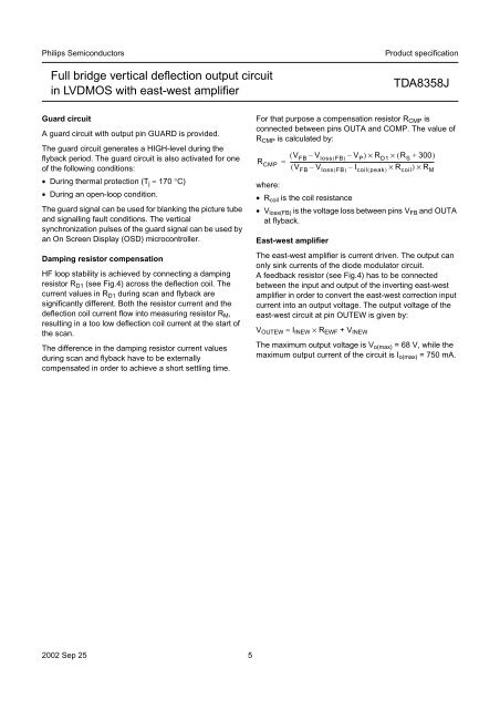
Philips Semiconductors<strong>Full</strong> <strong>bridge</strong> <strong>vertical</strong> <strong>deflection</strong> <strong>output</strong> <strong>circuit</strong><strong>in</strong> LVDMOS with east-west amplifierProduct specification<strong>TDA8358J</strong>Guard <strong>circuit</strong>A guard <strong>circuit</strong> with <strong>output</strong> p<strong>in</strong> GUARD is provided.The guard <strong>circuit</strong> generates a HIGH-level dur<strong>in</strong>g theflyback period. The guard <strong>circuit</strong> is also activated for oneof the follow<strong>in</strong>g conditions:• Dur<strong>in</strong>g thermal protection (T j ≈ 170 °C)• Dur<strong>in</strong>g an open-loop condition.The guard signal can be used for blank<strong>in</strong>g the picture tubeand signall<strong>in</strong>g fault conditions. The <strong>vertical</strong>synchronization pulses of the guard signal can be used byan On Screen Display (OSD) microcontroller.Damp<strong>in</strong>g resistor compensationHF loop stability is achieved by connect<strong>in</strong>g a damp<strong>in</strong>gresistor R D1 (see Fig.4) across the <strong>deflection</strong> coil. Thecurrent values <strong>in</strong> R D1 dur<strong>in</strong>g scan and flyback aresignificantly different. Both the resistor current and the<strong>deflection</strong> coil current flow <strong>in</strong>to measur<strong>in</strong>g resistor R M ,result<strong>in</strong>g <strong>in</strong> a too low <strong>deflection</strong> coil current at the start ofthe scan.The difference <strong>in</strong> the damp<strong>in</strong>g resistor current valuesdur<strong>in</strong>g scan and flyback have to be externallycompensated <strong>in</strong> order to achieve a short settl<strong>in</strong>g time.For that purpose a compensation resistor R CMP isconnected between p<strong>in</strong>s OUTA and COMP. The value ofR CMP is calculated by:( VR FB – V loss( FB)– V P ) × R D1 ×( R S + 300)CMP = -------------------------------------------------------------------------------------------------------------( V FB– V loss( FB)– I coil( peak)× R coil) × R Mwhere:• R coil is the coil resistance• V loss(FB) is the voltage loss between p<strong>in</strong>s V FB and OUTAat flyback.East-west amplifierThe east-west amplifier is current driven. The <strong>output</strong> canonly s<strong>in</strong>k currents of the diode modulator <strong>circuit</strong>.A feedback resistor (see Fig.4) has to be connectedbetween the <strong>in</strong>put and <strong>output</strong> of the <strong>in</strong>vert<strong>in</strong>g east-westamplifier <strong>in</strong> order to convert the east-west correction <strong>in</strong>putcurrent <strong>in</strong>to an <strong>output</strong> voltage. The <strong>output</strong> voltage of theeast-west <strong>circuit</strong> at p<strong>in</strong> OUTEW is given by:V OUTEW ≈ I INEW × R EWF +V INEWThe maximum <strong>output</strong> voltage is V o(max) = 68 V, while themaximum <strong>output</strong> current of the <strong>circuit</strong> is I o(max) = 750 mA.2002 Sep 25 5


