SJ-EN Instruction Manual - Hitachi America, Ltd.
SJ-EN Instruction Manual - Hitachi America, Ltd. SJ-EN Instruction Manual - Hitachi America, Ltd.
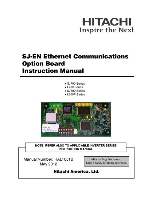
SJ-EN Ethernet CommunicationsOption BoardInstruction ManualSJ700 SeriesL700 SeriesSJ300 SeriesL300P SeriesNOTE: REFER ALSO TO APPLICABLE INVERTER SERIESINSTRUCTION MANUALManual Number: HAL1051BMay 2012After reading this manual,keep it handy for future reference.Hitachi America, Ltd.
- Page 2 and 3: NOTES:
- Page 4 and 5: Table of ContentsNOTES:Page 4 of 46
- Page 6 and 7: Chapter 1SAFETY PRECAUTIONSHIGH VOL
- Page 8 and 9: Chapter 1NOTES:Page 8 of 46
- Page 10 and 11: Chapter 2Installing the Option Boar
- Page 12 and 13: Chapter 2NOTES:Page 12 of 46
- Page 14 and 15: Chapter 3Figure 3-1 NetEdit3 Initia
- Page 16 and 17: Chapter 3Figure 3-2 NetEdit3 Screen
- Page 18 and 19: Chapter 4Chapter 4 - OperationSetti
- Page 20 and 21: Chapter 5Chapter 5 - Troubleshootin
- Page 22 and 23: AppendixAppendix - Parameter ListNo
- Page 24 and 25: AppendixF - Main Profile FunctionsF
- Page 26 and 27: AppendixA057 113 114 DC braking for
- Page 28 and 29: AppendixB006 1011 1012 Phase loss d
- Page 30 and 31: AppendixB113 1225 1226 Free V/F con
- Page 32 and 33: AppendixC123 2245 2246 [O2] input z
- Page 34 and 35: AppendixP - Expansion Card Function
- Page 36 and 37: AppendixPARAMETER LISTS FOR SJ700/L
- Page 38 and 39: AppendixA094 0187 0188 Selection of
- Page 40 and 41: AppendixC053 2105 2106 PID FBV func
- Page 42 and 43: AppendixP033 6065 6066 Torque sourc
- Page 44 and 45: IndexRR - Reference Codes · 36Regi
- Page 46: Hitachi America, Ltd.Tarrytown, NY
<strong>SJ</strong>-<strong>EN</strong> Ethernet CommunicationsOption Board<strong>Instruction</strong> <strong>Manual</strong><strong>SJ</strong>700 SeriesL700 Series<strong>SJ</strong>300 SeriesL300P SeriesNOTE: REFER ALSO TO APPLICABLE INVERTER SERIESINSTRUCTION MANUAL<strong>Manual</strong> Number: HAL1051BMay 2012After reading this manual,keep it handy for future reference.<strong>Hitachi</strong> <strong>America</strong>, <strong>Ltd</strong>.
NOTES:
Table of ContentsTable of ContentsTable of Contents ................................................................................................................... 3Chapter 1 – General Description .......................................................................................... 5Chapter 2 – Installation and Wiring ...................................................................................... 9Chapter 3 – Configuration................................................................................................... 13Chapter 4 – Operation ......................................................................................................... 18Chapter 5 – Troubleshooting .............................................................................................. 20Appendix – Parameter List ................................................................................................. 21Index ..................................................................................................................................... 43Page 3 of 46
Table of ContentsNOTES:Page 4 of 46
Chapter 1Chapter 1 – General DescriptionThe <strong>SJ</strong>-<strong>EN</strong> option board is an Ethernet communication interface for <strong>Hitachi</strong> <strong>SJ</strong>700, L700, <strong>SJ</strong>300 and L300Pseries AC variable frequency inverters. The board can be installed in either of the two available option slots inthe applicable inverter.The <strong>SJ</strong>-<strong>EN</strong> uses the open MODBUS/TCP communication protocol. It utilizes a 10Base-T physical interfacewith a 10 Mbps data transfer rate. Even though the board uses the MODBUS/TCP, this does not mean that allMODBUS services and functions are supported. Detailed description of the available functionality is providedin Chapter 4 of this manual. The board will act as a MODBUS/TCP slave that can be read from and written toover the Ethernet network from a MODBUS/TCP master device. It will not initiate communication with otherdevices on the network. It will only respond to requests from a master device. The <strong>SJ</strong>-<strong>EN</strong> will allow a user tocontrol the operation of the inverter, monitor its operation, and modify parameters.Before using this product, please read this manual and the relevant inverter manual, and be sure to follow allsafety precautions noted therein. After unpacking the <strong>SJ</strong>-<strong>EN</strong> board, carefully inspect it for any defect or damage,and be sure all parts are present.Carton Contents(1) <strong>SJ</strong>-<strong>EN</strong> Ethernet Communication Interface Board(2) Screws to secure board to inverter case (M3 x 8mm)(1) CD-ROM containing this manual (pdf) and NetEdit3 softwareWARRANTYThe warranty period under normal installation and handling conditions shall be eighteen (18) monthsfrom the date of purchase, or twelve (12) months from the date of installation, whichever occurs first.The warranty shall cover repair or replacement, at <strong>Hitachi</strong>’s sole discretion, of the <strong>SJ</strong>-<strong>EN</strong> Option board.Service in the following cases, even within the warranty period, shall be to the customers account:1. Malfunction or damage caused by misuse, modification or unauthorized repair.2. Malfunction or damage caused by mishandling, dropping, etc., after delivery.3. Malfunction or damage caused by fire, earthquake, flood, lightning, abnormal input voltage,contamination, or other natural disasters.If service is required for the product at your worksite, all expenses associated with field repair are thepurchaser’s responsibility. This warranty only covers service at <strong>Hitachi</strong> designated service facilities.If making a warranty claims in reference to the above, please contact the distributor from whom youpurchased the <strong>SJ</strong>-<strong>EN</strong>, and provide the model number, purchase date, installation date, and description ofdamage or missing components.Page 5 of 46
Chapter 1SAFETY PRECAUTIONSHIGH VOLTAGE: This symbol indicates high voltage. It calls your attention to items or operationsthat could be dangerous to you and other persons operating this equipment. Read the message andfollow the instructions carefully.WARNING: Indicates a potentially hazardous situation that, if not avoided, can result in seriousinjury or death.CAUTION: Indicates a potentially hazardous situation that, if not avoided, can result in minor tomoderate injury, or serious damage to the product. The situation described in the CAUTION may, ifnot avoided, lead to serious results. Important safety measures are described in CAUTION (as well asWARNING), so be sure to observe them.HIGH VOLTAGE: Motor control equipment and electronic controllers are connected to hazardousline voltages. When servicing drives and electronic controllers, there may be exposed componentswith housings or protrusions at or above line potential. Extreme care should be taken to protectagainst shock. Stand on an insulating pad and make it a habit to use only one hand when checkingcomponents. Always work with another person in case an emergency occurs. Disconnect powerbefore checking controllers or performing maintenance. Be sure equipment is properly grounded.Wear safety glasses whenever working on electronic controllers or rotating machinery.WARNING: This equipment should be installed, adjusted, and serviced by qualified electricalmaintenance personnel familiar with the construction and operation of the equipment and the hazardsinvolved. Failure to observe this precaution could result in bodily injury.WARNING: HAZARD OF ELECTRICAL SHOCK. DISCONNECT INCOMING POWERBEFORE WORKING ON THIS CONTROL.WARNING: Wait at least five (5) minutes after turning OFF the input power supply beforeperforming maintenance or an inspection. Otherwise, there is the danger of electric shock.WARNING: Do not install or remove the <strong>SJ</strong>-<strong>EN</strong> Ethernet option board while the inverter isenergized. Otherwise there is the danger of electric shock and/or fire.WARNING: Never modify the unit. Otherwise, there is a danger of electric shock and/or injury.CAUTION: Be sure to secure the <strong>SJ</strong>-<strong>EN</strong> option board with the supplied mounting screws. Make sureall connections are made securely; otherwise there is danger of a loose connection and unpredictableoperation.CAUTION: Alarm connection may contain hazardous live voltage even when inverter isdisconnected. When removing the front cover for maintenance or inspection, confirm that incomingpower for alarm connection is completely disconnected.Page 6 of 46
Chapter 1CAUTION: Be sure not to touch the surface or terminals of the <strong>SJ</strong>-<strong>EN</strong> Ethernet option board whilethe inverter is energized; otherwise there is the danger of electric shock.CAUTION: The software lock modes described in the <strong>SJ</strong>300 inverter manual are NOT supported viathe <strong>SJ</strong>-<strong>EN</strong> option board. This means that network commands can bypass any software lock settingsconfigured via the inverter keypad. It is incumbent on the user to make sure no safety lockouts areviolated through network commands.CAUTION: When configuring parameters with the standard keypad, the inverter checks for andinhibits invalid parameter combinations when the STR key is pressed. The <strong>SJ</strong>-<strong>EN</strong> bypasses this check,so it is incumbent on the user to make sure invalid configuration parameters or combinations are notsent through network commands. Otherwise undesirable inverter behavior may occur.CAUTION: Certain parameter data ranges vary depending on model and capacity. The <strong>SJ</strong>-<strong>EN</strong> doesNOT check to make sure these data are within range. It is incumbent on the user to make sure data forthese parameters is within range for the specific model and rating. These parameters are noted in theparameter tables in the Appendix. Otherwise undesirable inverter behavior may occur.INVERTER COMPATIBILITYThe <strong>SJ</strong>-<strong>EN</strong> Ethernet Interface option board is compatible only with <strong>SJ</strong>700, L700, <strong>SJ</strong>300 and L300P seriesinverters. However, the parameters that can be accessed are different for the 700 and 300 series inverters. Thetables at the end of this manual show which parameters are accessible for each.Page 7 of 46
Chapter 1NOTES:Page 8 of 46
Chapter 2Chapter 2 – Installation and WiringOrientation to Product FeaturesFigure 2-1 below shows the physical layout of the <strong>SJ</strong>-<strong>EN</strong> Ethernet option board. In particular, note the locationof status LEDs and DIP-switches.STATUS LEDsSTATUSLINKACTIVITYERRORRJ45JackConnector toconnect to<strong>SJ</strong>300 or L300P(rear of board)7 6 5 4 3 2 1 0 ONRXD LED<strong>SJ</strong>-<strong>EN</strong>DIP SwitchesOFFTXD LEDFigure 2-1<strong>SJ</strong>-<strong>EN</strong> LayoutThe pinout for the RJ45 connector is as follows:1. TX Data +2. TX Data –3. RX Data +4. NC5. NC6. RX Data –7. NC8. NC8 7 6 5 4 3 2 1Figure 2-2<strong>SJ</strong>-<strong>EN</strong> RJ45 PinoutsPage 9 of 46
Chapter 2Installing the Option BoardPower down the inverter and wait at least five minutes before moving to the next step. Open and remove thelower terminal cover. Confirm that the red CHARGE LED is extinguished and that the DC bus is fullydischarged before proceeding further, otherwise there is the danger of electric shock. Then remove keypad fromthe inverter. You can now remove the upper front cover to expose the two option ports inside.Figure 2-3 below shows how to install the option board to option port 1 or 2 of the inverter. There are four holeson the corners of the option board. Align the board with the port connector in the proper orientation (to the left,when facing the inverter as show). Then align the top two holes with the two screw holes, and the bottom twoholes with the two guide posts. Insert the board fully into the connector. Secure the board with the two M3screws supplied.Option boardGuide posts foroption board positioningOption port 1Option port 2Screw holes for securing the option board(M3 screws x 2)Figure 2-3Installation of <strong>SJ</strong>-<strong>EN</strong>Page 10 of 46
Chapter 2User InterfaceThe <strong>SJ</strong>-<strong>EN</strong> has six LEDs to convey module status and activity.Four LEDs next to the RJ45 connector:STATUS (GRE<strong>EN</strong>) – This LED will be ON whenever the <strong>SJ</strong>-<strong>EN</strong> is receiving proper power from theinverter and the self diagnostics have shown the board to be functioning normally.LINK (GRE<strong>EN</strong>) – This LED is ON when the <strong>SJ</strong>-<strong>EN</strong> is receiving valid Ethernet pulses.ACTIVITY (GRE<strong>EN</strong>) – This LED is ON whenever there is Ethernet traffic in the cable.ERROR (RED) – This LED will be ON if the <strong>SJ</strong>-<strong>EN</strong> has failed due to a hardware watchdog timeout, orthe Ethernet communications has been absent for the software watchdog timeout period.Two LEDs near the right edge of the board:TXD – This LED indicates communication from the <strong>SJ</strong>-<strong>EN</strong> to the inverter through the option port.RXD – This LED indicates communication to the <strong>SJ</strong>-<strong>EN</strong> from the inverter through the option port.(These two LEDs may appear blinking or may appear steady ON due to the high blink rate.)Page 11 of 46
Chapter 2NOTES:Page 12 of 46
Chapter 3Chapter 3 – ConfigurationInstall NetEdit3 SoftwareNetEdit3 Software is provided on the CD-R enclosed with the <strong>SJ</strong>-<strong>EN</strong> option board. It can also be downloaded atno cost from <strong>Hitachi</strong> <strong>America</strong>’s web site (www.hitachi-america.us/inverters). This software is required toconfigure the board. It can also be used to update the <strong>SJ</strong>-<strong>EN</strong> firmware in the event of a future update. NetEdit3is compatible with Microsoft Windows 98, Windows ME, Windows 2000, Windows XP, and Windows NT4.In Windows, run the program “SetupNE3.exe” on the CD-R to install the program. Follow the on-screeninstructions to complete the installation.Configuration of the <strong>SJ</strong>-<strong>EN</strong> BoardEnsure that the <strong>SJ</strong>-<strong>EN</strong> is properly installed as described in Chapter 2. Attach a standard Ethernet Crossover cableto the RJ45 connector on the <strong>SJ</strong>-<strong>EN</strong>. Connect the other end to the RJ45 port of a Windows PC with an Ethernetadapter installed. If connecting the <strong>SJ</strong>-<strong>EN</strong> to a hub, switch or router, use a patch (straight-through) cable instead.For best results, use Category 5, commercial quality cables rated for 10BaseT applications.There are 8 DIP-switches on the <strong>SJ</strong>-<strong>EN</strong> board (see Figure 2-1). Switches 6 and 7 are not used. Switches 0 to 5may be used to set a 6-bit binary number representing 000001 to 111111 binary or 1 to 63 in decimal, for adevice (module) ID. However, for normal Modbus/TCP use, switches 0-5 should all be set to ZERO (off). Whenconfigured that way, the device ID is obtained from board’s FLASH memory. The value will be programmedinto the <strong>SJ</strong>-<strong>EN</strong> flash memory by means of the NetEdit3 software; this ID can be any 32-bit binary value (i.e. 0 to4,294,967,295 decimal).Make sure that all wiring is secure in the inverter, and that the power connections are free and clear. Be sure toseparate power wiring from control wiring. If they have to be crossed, be sure that they cross at a right angle.Connect the inverter to the PC Ethernet port, and that the PC is started and running Windows. Power up theinverter, and observe the LEDs on the <strong>SJ</strong>-<strong>EN</strong> board. The STATUS LED should be illuminated, and the LINK,ACTIVITY, RXD and TXD LEDs should be blinking (may appear as though ON continuously, due to high blinkrate). The red ERROR LED should NOT be illuminated. See Chapter 4 for detailed description of LEDfunctions. If the LED conditions are not correct, proceed to Chapter 5 for Troubleshooting. If you power up theinverter before powering up the PC, an error code may appear. After powering up the PC and properlyconnecting the cable, you should be able to clear the error with the STOP/RESET key on the inverter keypad.If the LEDs are correct, power down the inverter again. After the inverter CHARGE LED has extinguished,replace the covers on the inverter and reinstall the keypad. Then you can power up the inverter and continuewith the configuration.Set Up the <strong>SJ</strong>-<strong>EN</strong> with NetEdit3With the inverter powered up and the Ethernet cable connected from the <strong>SJ</strong>-<strong>EN</strong> to your PC, launch the NetEdit3program. Figure 3-1 shows the initial screen on program start-up. Should an error code appear on the inverterdisplay at power-up, simply press the STOP/RESET key on the keypad to clear it.Page 13 of 46
Chapter 3Figure 3-1 NetEdit3 Initial ScreenThe NetEdit3 software should find and list any <strong>SJ</strong>-<strong>EN</strong> attached to the network. If not, just click on “ScanPage 14 of 46
Chapter 3Network”. An entry will appear in the Device List (grid area), with the board details as shown in Figure 3-2. Ifmore than one board is connected in a common network, you will see a line entry for each of them. The“Module Info” and “General Settings” tabs will now also appear next to the “General Help” tab, below theDevice List. You can then click on the line for the board you wish to configure, and click on the “GeneralSettings” tab and then the “General” button to bring up the General Settings dialog box containing the devicedetails, or you can simply double-click on the device in the Device List. In the General Settings dialog box(Figure 3-3), you can enter the Module ID for the device, provided the DIP Switches on the board are all set tozero. Otherwise, the Module ID will reflect the DIP switch setting, and will be grayed out, indicating it cannotbe modified with NetEdit3. You can also input a Name for the device, and a Description. The default Name willbe “<strong>Hitachi</strong> Drive”, and the default Description will be “<strong>SJ</strong>300/L300P <strong>Hitachi</strong> Drive”.The device’s IP Address will also be shown. Change this to the desired IP address for your Modbus/TCPnetwork. Your master device will need this address to communicate with this node. Note that all <strong>SJ</strong>-<strong>EN</strong> boardsship with the default IP address of “255.255.255.255”. When you change the IP address, the NetEdit3 softwaremay no longer be able to see it in TCP/IP mode if the PC’s IP address is not on the same sub-network. You cancommunicate to the <strong>SJ</strong>-<strong>EN</strong> despite this using the IPX mode, however you will have to make sure IPX support isinstalled in Windows on that PC.Once you have made the necessary changes, you can exit NetEdit3, and disconnect the cable from your PC tothe <strong>SJ</strong>-<strong>EN</strong> board. You may now connect the <strong>SJ</strong>-<strong>EN</strong> to your network to begin normal operation.Page 15 of 46
Chapter 3Figure 3-2 NetEdit3 Screen after Scan of NetworkFigure 3-3 NetEdit3 General SettingsDialog BoxPage 16 of 46
Chapter 3NOTES:Page 17 of 46
Chapter 4Chapter 4 – OperationSetting Up the Inverter for Ethernet Network OperationOnce the <strong>SJ</strong>-<strong>EN</strong> board has been properly configured and connected to a network as described in Chapter 3, it iscapable of reading data from and writing data to the inverter. However if it is desired to have either the RUNcommand and/or the speed reference come from the Ethernet master, you must change two inverter parametersas shown in the following table.FunctionCodeNameDescriptionRunModeEditLo Hi–FE(EU)Defaults–FU(US)–FR(Jpn)Setting for Ethernet ControlA001FrequencySourceSettingSix options; select codes:00 Keypad potentiometer01Control terminal02 Function F001 setting03 RS485 serial command04 Expansion board 105 Expansion board 2 01 01 02 02A002Runcommandsource settingFive options; select codes:01 Input terminal [FW] or [RV](assignable)02 Run key on keypad, ordigital operator03 RS485 serial command04 Start/Stop, expansion card #105 Start/Stop, expansion card #2 01 01 02 02Supported MODBUS FunctionsThe <strong>SJ</strong>-<strong>EN</strong> is implemented with the MODBUS/TCP communication protocol. It supports the followingMODBUS functions:READ MULTIPLE REGISTERS (03) – This function reads the contents of a contiguous blockof holding registers in the inverter.READ INPUT REGISTERS (04) – This function reads from 1 to up to around 125 contiguousinput registers in the inverter.WRITE SINGLE REGISTER (06) – This function will write to a single holding register in theinverter.WRITE MULTIPLE REGISTERS (16) – This function will write to a block of contiguousregisters in the inverter.Additional MODBUS/TCP protocol details, including specifications, application information, implementationguides, and other resources are available from the web site www.modbus.org.Page 18 of 46
Chapter 4NOTES:Page 19 of 46
Chapter 5Chapter 5 – TroubleshootingIn general, the first step to troubleshooting should be to inspect the status LEDs on the <strong>SJ</strong>-<strong>EN</strong> board, in additionto the inverter operator/keypad display. These will give valuable clues to the nature of the problem.In addition, the inverter operator/keypad will provide diagnostic information for certain types of errors. Errorcodes for the option boards will have the format of: for a board installed in option slot 1, or for a board installed in option slot 2. The numberto the right of the decimal point indicates the drive status at the time of trip, as follows:At reset At stop At constant speed At startingDuringdecelerationDuringacceleration f0 StopDuring DCinjectionbrakingDuring overloadrestrictionThe digit immediately to the left of the decimal point has the following meaning:Code Trip Name Cause Check RemedyEthernet CommunicationErrorInternal CommunicationError (between <strong>SJ</strong>-<strong>EN</strong> andinverter)Inverter Mismatch(blinking display asshown)DefectiveconnectionPC not powered upor not connected toinverterNetworkconfiguration errorOption board ajar orlooseBoard lockupPage 20 of 46Connectors (plugs& jacks), cableThat PC is poweredon and connectedVerify properEthernet setup of<strong>SJ</strong>-<strong>EN</strong> and masterdeviceVerify board isproperly seated inconnectorCheck status LEDsReplace or repair;press STOP/RESETon inverter keypadPress STOP/RESETon inverter keypadReconfigureincorrect settings.Remove and reseatboardPress STOP/RESETkey on inverter orcycle powerBoard defective Check status LEDs Replace <strong>SJ</strong>-<strong>EN</strong>Inverter firmwareversion notcompatible with<strong>SJ</strong>-<strong>EN</strong> option boardInverterManufacturingNumber for version(see Page 7)Replace Inverterwith later version
AppendixNOTES:Page 21 of 46
AppendixAppendix – Parameter ListNote: Parameters in BOLDFACE can be edited while inverter is in the RUN mode. “RO” means theparameter is Read Only, and “R/W” means the value can be read or written.InverterParameterModbusStartAddressModbusEndAddressParameter NameMagnitudeRead/WriteData RangeD – Monitoring FunctionsD001 3001 3002 Output frequency monitor X1000 RO 0 – 400000D002 3003 3004 Output current monitor X10 RO 0 – 10000D003 3005 3006 Rotation direction monitor X1 RO 0 – 2D004 3007 3008Process Variable (PV) PIDfeedback monitorX100 RO 0 – 999900D005 3009 3010 Intelligent input terminal status X1 RO 0 – 65535D006 3011 3012 Intelligent output terminal status X1 RO 0 – 65535D007 3013 3014 Scaled output frequency monitor X1000 RO 0 – 39960000D012 3023 3024 Output torque monitor X1 RO –300 – 300D013 3025 3026 Output voltage monitor X10 RO 0 – 10000D014 3027 3028 Input electric power monitor X10 RO 0 – 10000D016 3031 3032 Cumulative RUN time monitor X1 ROD017 3033 3034 Cumulative power–on time X1 RO0 –42948362250 –4294836225D078 ‡ 3155 3156 Last trip pointer X1 RO 0 – 5D080 ‡ 3159 3160 Trip counter X1 RO 0 – 65535D081 3161 3162 Error Code of Trip 1 X1 RO 0 – 255D355 ‡ 3709 3710 Frequency at Trip 1 X100 RO 0 – 40000D356 ‡ 3711 3712 Output current at Trip 1 X10 RO 0 – 10000D357 ‡ 3713 3714 PN voltage (DC voltage) at Trip 1 X10 RO 0 – 10000D358 ‡ 3715 3716 Cumulative RUN time at Trip 2 X1 ROD359 ‡ 3717 3718 Cumulative power–on time at Trip 2 X1 RO0 –42948362250 –4294836225D082 3163 3164 Error Code of Trip2 X1 RO 0 – 255D361 ‡ 3721 3722 Frequency at Trip 2 X100 RO 0 – 40000D362 ‡ 3723 3724 Output current of Trip 2 X10 RO 0 – 10000D363 ‡ 3725 3726 PN voltage (DC voltage) at Trip2 X10 RO 0 – 10000D364 ‡ 3727 3728 Cumulative RUN time at Trip 2 X1 ROD365 ‡ 3729 3730 Cumulative power–on time at Trip 2 X1 RO0 –42948362250 –4294836225D083 3165 3166 Error Code of Trip 3 X1 RO 0 – 255Page 22 of 46
AppendixD367 ‡ 3733 3734 Frequency at Trip 3 X100 RO 0 – 40000D368 ‡ 3735 3736 Output current at Trip3 X10 RO 0 – 10000D369 ‡ 3737 3738 PN voltage (DC voltage) at Trip 3 X10 RO 0 – 10000D370 ‡ 3739 3740 Cumulative RUN time at Trip 3 X1 ROD371 ‡ 3741 3742 Cumulative power–on time at Trip 3 X1 RO0 –42948362250 –4294836225D084 3167 3168 Error Code of Trip 4 X1 RO 0 – 255D373 ‡ 3745 3746 Frequency at Trip 4 X100 RO 0 – 40000D374 ‡ 3747 3748 Output current at Trip 4 X10 RO 0 – 10000D375 ‡ 3749 3750 PN voltage (DC voltage) at Trip 4 X10 RO 0 – 10000D376 ‡ 3751 3752 Cumulative RUN time at Trip 4 X1 ROD377 ‡ 3753 3754 Cumulative power–on time at Trip 4 X1 RO0 –42948362250 –4294836225D085 3169 3170 Error Code of Trip 5 X1 RO 0 – 255D379 ‡ 3757 3758 Frequency at Trip 5 X100 RO 0 – 40000D380 ‡ 3759 3760 Output current at Trip 5 X10 RO 0 – 10000D381 ‡ 3761 3762 PN voltage (DC voltage) at Trip 5 X10 RO 0 – 10000D382 ‡ 3763 3764 Cumulative RUN time at Trip 5 X1 ROD383 ‡ 3765 3766 Cumulative power–on time at Trip 5 X1 RO0 –42948362250 –4294836225D086 3171 3172 Error Code of Trip 6 X1 RO 0 – 255D385 ‡ 3769 3770 Frequency at Trip 6 X100 RO 0 – 40000D386 ‡ 3771 3772 Output current at Trip 6 X10 RO 0 – 10000D387 ‡ 3773 3774 PN voltage (DC voltage) at Trip 6 X10 RO 0 – 10000D388 ‡ 3775 3776 Cumulative RUN time at Trip 6 X1 ROD389 ‡ 3777 3778 Cumulative power–on time at Trip 6 X1 RO0 –42948362250 –4294836225D101 ‡ 3201 3202 Output Frequency Monitor X1000 RO 0 – 400000D102 ‡ 3203 3204 DC Bus Voltage X10 RO 1 – 10000D103 ‡ 3205 3206 Accumulated BRD ON time X10 RO 1 – 1000D104 ‡ 3207 3208 E-Thermal Monitor X10 RO 1 – 1000D106 ‡ 3211 3212 MCU Version X1 RO 0 – 65535Page 23 of 46
AppendixF – Main Profile FunctionsF001 4001 4002Output frequency setting(Hz) /PID Setpoint (%)X1000 RO 0 – 400000F002 4003 4004 Acceleration time 1 X100 R/W 1 – 360000F202 4403 4404 Acceleration time 1, 2 nd motor X100 R/W 1 – 360000F302 4603 4604 Acceleration time 1, 3 rd motor X100 R/W 1 – 360000F003 4005 4006 Deceleration time 1 X100 R/W 1 – 360000F203 4405 4406 Deceleration time 1, 2 nd motor X100 R/W 1 – 360000F303 4605 4606 Deceleration time 1, 3 rd motor X100 R/W 1 – 360000F004 4007 4008 Keypad RUN key routing X1 R/W 0 – 1A – Standard FunctionsA001 1 2 Frequency source setting X1 R/W 0 – 5A002 3 4 Run command source setting X1 R/W 1 – 5A003 5 6 Base frequency setting X1 R/W 30 – 400A203 405 406 Base frequency setting, 2 nd motor X1 R/W 30 – 400A303 605 606 Base frequency setting, 3 rd motor X1 R/W 30 – 400A004 7 8 Maximum frequency setting X1 R/W 30 – 400A204 407 408A304 607 608Maximum frequency setting, 2 ndmotorMaximum frequency setting, 3 rdmotorX1 R/W 30 – 400X1 R/W 30 – 400A005 9 10 [AT] selection X1 R/W 0 – 1A006 11 12 [O2] selection X1 R/W 0 – 3A011 21 22A012 23 24A013 25 26A014 27 28[O]–[L] input active range startfrequency[O]–[L] input active range endfrequency[O]–[L] input active range startvoltage[O]–[L] input active range endvoltageX100 R/W 0 – 40000X100 R/W 0 – 40000X1 R/W 0 – 100X1 R/W 0 – 100A015 29 30 [O]–[L] input start frequency select X1 R/W 0 – 1A016 31 32 Analog input filter time constant X1 R/W 1 – 30A019 37 38 Multi–speed operation selection X1 R/W 0 – 1A020 39 40 Multi–speed frequency 0 X100 R/W 0 – 40000A220 439 440A320 639 640Multi–speed frequency 0, 2 ndmotorMulti–speed frequency 0, 3 rdmotorX100 R/W 0 – 40000X100 R/W 0 – 40000A021 41 42 Multi–speed frequency 1 X100 R/W 0 – 40000Page 24 of 46
AppendixA022 43 44 Multi–speed frequency 2 X100 R/W 0 – 40000A023 45 46 Multi–speed frequency 3 X100 R/W 0 – 40000A024 47 48 Multi–speed frequency 4 X100 R/W 0 – 40000A025 49 50 Multi–speed frequency 5 X100 R/W 0 – 40000A026 51 52 Multi–speed frequency 6 X100 R/W 0 – 40000A027 53 54 Multi–speed frequency 7 X100 R/W 0 – 40000A028 55 56 Multi–speed frequency 8 X100 R/W 0 – 40000A029 57 58 Multi–speed frequency 9 X100 R/W 0 – 40000A030 59 60 Multi–speed frequency 10 X100 R/W 0 – 40000A031 61 62 Multi–speed frequency 11 X100 R/W 0 – 40000A032 63 64 Multi–speed frequency 12 X100 R/W 0 – 40000A033 65 66 Multi–speed frequency 13 X100 R/W 0 – 40000A034 67 68 Multi–speed frequency 14 X100 R/W 0 – 40000A035 69 70 Multi–speed frequency 15 X100 R/W 0 – 40000A038 75 76 Jog frequency setting X100 R/W 0 – 999A039 77 78 Jog stop mode X1 R/W 0 – 5A041 81 82 Torque boost method selection X1 R/W 0 – 1A241 481 482 Torque boost method, 2 nd motor X1 R/W 0 – 1A042 83 84 <strong>Manual</strong> torque boost value X10 R/W 0 – 200A242 483 484A342 683 684A043 85 86A243 485 486A343 685 686A044 87 88A244 487 488A344 687 688<strong>Manual</strong> torque boost value, 2 ndmotor<strong>Manual</strong> torque boost value 3 rdmotor<strong>Manual</strong> torque boost frequencyadjustment<strong>Manual</strong> torque boost frequencyadjustment, 2 nd motor<strong>Manual</strong> torque boost frequency,3 rd motorV/f characteristic curve selection,1 st motorV/f characteristic curve selection,2 nd motorV/f characteristic curve selection,3 rd motorX10 R/W 0 – 200X10 R/W 0 – 200X10 R/W 0 – 500X10 R/W 0 – 500X10 R/W 0 – 500X1 R/W 0 – 5 *X1 R/W 0 – 4 *X1 R/W 0 – 1A045 89 90 V/f gain setting X1 R/W 20 – 100A051 101 102 DC braking enable X1 R/W 0 – 1A052 103 104 DC braking frequency setting X100 R/W 0 – 6000A053 105 106 DC braking wait time X10 R/W 0 – 50A054 107 108DC braking force duringdecelerationX1 R/W 0 – 100 *A055 109 110 DC braking time for deceleration X10 R/W 0 – 600A056 111 112Selection of edge/level action of DCbraking input [DB]X1 R/W 0 – 1Page 25 of 46
AppendixA057 113 114 DC braking force for starting X1 R/W 0 – 100 *A058 115 116 DC braking time for starting X10 R/W 0 – 600A059 117 118 DC braking carrier frequency X10 R/W 5 – 150 *A061 121 122 Frequency upper limit setting X100 R/W 0 – 40000A261 521 522Frequency upper limit setting, 2 ndmotorPage 26 of 46X100 R/W 0 – 40000A062 123 124 Frequency lower limit setting X100 R/W 0 – 40000A262 523 524Frequency lower limit setting, 2 ndmotorX100 R/W 0 – 40000A063 125 126 Jump frequency 1 X100 R/W 0 – 40000A064 127 128 Width of jump frequency 1 X100 R/W 0 – 1000A065 129 130 Jump frequency 2 X100 R/W 0 – 40000A066 131 132 Width of jump frequency 2 X100 R/W 0 – 1000A067 133 134 Jump frequency 3 X100 R/W 0 – 40000A068 135 136 Width of jump frequency 3 X100 R/W 0 – 1000A069 137 138Acceleration pause frequencysettingX100 R/W 0 – 40000A070 139 140 Acceleration pause time setting X10 R/W 0 – 600A071 141 142 PID Enable X1 R/W 0 – 1A072 143 144 PID Proportional(P) gain X10 R/W 2 – 50A073 145 146 PID Integral (I) time constant X10 R/W 0 – 36000A074 147 148 PID Derivative (D) time constant X100 R/W 0 – 10000A075 149 150 PID PV Scale conversion X100 R/W 1 – 9999A076 151 152 PID PV source setting X1 R/W 0 – 1A081 161 162 AVR function select X1 R/W 0 – 2A082 163 164 AVR voltage select X1 R/W0 = 200 V *1 = 215 V2 = 220 V3 = 230 V4 = 240 V5 = 380 V6 = 400 V7 = 415 V8 = 440 V9 = 460 V10 = 480 VA085 169 170 Operation mode selection X1 R/W 0 – 2 *A086 171 172 Energy saving mode tuning X10 R/W 0 – 1000A092 183 184 Acceleration time (2) X100 R/W 1 – 360000A292 583 584 Acceleration time (2), 2 nd motor X100 R/W 1 – 360000A392 783 784 Acceleration time (2), 3 rd motor X100 R/W 1 – 360000A093 185 186 Deceleration time (2) X100 R/W 1 – 360000A293 585 586 Deceleration time (2), 2 nd motor X100 R/W 1 – 360000A393 785 786 Deceleration time (2), 3 rd motor X100 R/W 1 – 360000
AppendixA094 187 188A294 587 588A095 189 190A295 589 590A096 191 192A296 591 592Select method to switch toacc2/dec2 profileSelect method to switch toacc2/dec2 profile, 2 nd motorAcc1 to Acc2 frequency transitionpointAcc1 to Acc2 frequency transitionpoint, 2 nd motorDec1 to Dec2 frequency transitionpointDec1 to Dec2 frequency transitionpoint, 2 nd motorX1 R/W 0 – 1X1 R/W 0 – 1X100 R/W 0 – 40000X100 R/W 0 – 40000X100 R/W 0 – 40000X100 R/W 0 – 40000A097 193 194 Acceleration curve selection X1 R/W 0 – 3A098 195 196 Deceleration curve selection X1 R/W 0 – 3A101 201 202A102 203 204A103 205 206A104 207 208A105 209 210A111 221 222A112 223 224A113 225 226A114 227 228[OI]–[L] input active range startfrequency[OI]–[L] input active range endfrequency[OI]–[L] input active range startcurrent[OI]–[L] input active range endcurrent[OI]–[L] input start frequencyenable[O2]–[L] input active range startfrequency[O2]–[L] input active range endfrequency[O2]–[L] input active range startvoltage[O2]–[L] input active range endvoltageX100 R/W 0 – 40000X100 R/W 0 – 40000X1 R/W 0 – 100X1 R/W 0 – 100X1 R/W 0 – 1X100X100R/WR/W–40000 –40000–40000 –40000X1 R/W –100 – 100X1 R/W –100 – 100A131 261 262 Acceleration curve constant X1 R/W 1 – 10A132 263 264 Deceleration curve constant X1 R/W 1 – 10B – Fine–Tuning FunctionsB001 1001 1002 Selection of automatic restart mode X1 R/W 0 – 3B002 1003 1004Allowable under–voltage powerfailure timeX10 R/W 3 – 250B003 1005 1006 Retry wait time before motor restart X10 R/W 3 – 1000B004 1007 1008B005 1009 1010Instantaneous powerfailure/under–voltage trip alarmenableNumber of restarts on powerfailure/under–voltage eventsX1 R/W 0 – 2X1 R/W 0 – 1Page 27 of 46
AppendixB006 1011 1012 Phase loss detection enable X1 R/W 0 – 1B007 1013 1014 Restart frequency threshold X100 R/W 0 – 40000B012 1023 1024B212 1423 1424B312 1623 1624B013 1025 1026B213 1425 1426B313 1625 1626B015 1029 1030B016 1031 1032B017 1033 1034B018 1035 1036B019 1037 1038B020 1039 1040B021 1041 1042Level of electronic thermal setting,1 st motorLevel of electronic thermal setting,2 nd motorLevel of electronic thermal setting,3 rd motorElectronic thermal characteristic, 1 stmotorElectronic thermal characteristic,2 nd motorElectronic thermal characteristic,3 rd motorFree setting electronic thermalfrequency 1Free setting electronic thermalcurrent 1Free setting electronic thermalfrequency 2Free setting electronic thermalcurrent 2Free setting electronic thermalfrequency 3Free setting electronic thermalcurrent 3Overload restriction operationmodePage 28 of 46X10 R/W 200 – 1200X10 R/W 200 – 1200X10 R/W 200 – 1200X1 R/W 0 – 2X1 R/W 0 – 2X1 R/W 0 – 2X1 R/W 0 – 400X10 R/W 0 – 10000X1 R/W 0 – 400X10 R/W 0 – 10000X1 R/W 0 – 400X10 R/W 0 – 10000X1 R/W 0 – 3B022 1043 1044 Overload restriction setting X10 R/W 500 – 2000 *B023 1045 1046B024 1047 1048Deceleration rate at overloadrestrictionSelection of method of overloadrestriction 2X100 R/W 10 – 3000X1 R/W 0 – 3B025 1049 1050 Overload restriction setting 2 X10 R/W 500 – 2000 *B026 1051 1052Deceleration rate at overloadrestriction 2X100 R/W 10 – 3000B031 1061 1062 Software lock mode selection X1 R/W 0 – 10B034 1067 1068 Run/power – on warning time X1 R/W 0 – 65535B035 1069 1070 Rotational direction restriction X1 R/W 0 – 2B036 1071 1072 Reduced voltage start selection X1 R/W 0 – 6B037 1073 1074 Function code display restriction X1 R/W 0 – 2B040 1079 1080 Torque limit selection X1 R/W 0 – 4B041 1081 1082 Torque limit (I) forward driving X1 R/W 0 – 200 *B042 1083 1084 Torque limit (II) reverse regen. X1 R/W 0 – 200 *B043 1085 1086 Torque limit (III) reverse driving X1 R/W 0 – 200 *B044 1087 1088 Torque limit (IV) forward regen. X1 R/W 0 – 200 *
AppendixB045 1089 1090 Torque limit LADSTOP enable X1 R/W 0 – 1B046 1091 1092 Reverse run protection enable X1 R/W 0 – 1B050 1099 1100B051 1101 1102B052 1103 1104B053 1105 1106B054 1107 1108B080 1159 1160B081 1161 1162Controlled deceleration and stop onpower lossDC bus voltage trigger level duringpower lossOver–voltage threshold duringpower lossDeceleration time setting duringpower lossInitial output frequency decreaseduring power loss[AM] terminal analog meteradjustment[FM] terminal analog meteradjustmentX1 R/W 0 – 1X10 R/W 0 – 10000X10 R/W 0 – 10000X100 R/W 1 – 360000X100 R/W 0 – 1000X1 R/W 0 – 255X1 R/W 0 – 255B082 1163 1164 Start frequency adjustment X100 R/W 10 – 999B083 1165 1166 Carrier frequency setting X10 R/W 5 – 150 *B084 1167 1168 Initialization mode X1 R/W 0 – 2B085 1169 1170 Country code for initialization X1 R/W 0 – 2B086 1171 1172 Frequency scaling factor X10 R/W 1 – 999B087 1173 1174 STOP key enable X1 R/W 0 – 1B088 1175 1176 Restart mode after FRS X1 R/W 0 – 1B090 1179 1180 Dynamic braking usage ratio X10 R/W 0 – 1000B091 1181 1182 Stop mode selection X1 R/W 0 – 1B092 1183 1184 Cooling fan control X1 R/W 0 – 1B095 1189 1190 Dynamic braking control X1 R/W 0 – 2B096 1191 1192 Dynamic braking activation level X1 R/W 330 – 760 *B098 1195 1196 Thermistor function X1 R/W 0 – 2B099 1197 1198 Thermistor protection level setting X1 R/W 0 – 9999B100 1199 1200 Free V/F control frequency 1 X1 R/W 0 – 400B101 1201 1202 Free V/F control voltage 1 X10 R/W 0 – 8000B102 1203 1204 Free V/F control frequency 2 X1 R/W 0 – 400B103 1205 1206 Free V/F control voltage 2 X10 R/W 0 – 8000B104 1207 1208 Free V/F control frequency 3 X1 R/W 0 – 400B105 1209 1210 Free V/F control voltage 3 X10 R/W 0 – 8000B106 1211 1212 Free V/F control frequency 4 X1 R/W 0 – 400B107 1213 1214 Free V/F control voltage 4 X10 R/W 0 – 8000B108 1215 1216 Free V/F control frequency 5 X1 R/W 0 – 400B109 1217 1218 Free V/F control voltage 5 X10 R/W 0 – 8000B110 1219 1220 Free V/F control frequency 6 X1 R/W 0 – 400B111 1221 1222 Free V/F control voltage 6 X10 R/W 0 – 8000B112 1223 1224 Free V/F control frequency 7 X1 R/W 0 – 400Page 29 of 46
AppendixB113 1225 1226 Free V/F control voltage 7 X10 R/W 0 – 8000B120 1239 1240 Brake control enable X1 R/W 0 – 1B121 1241 1242 Brake wait time for release X100 R/W 0 – 500B122 1243 1244 Brake wait time for acceleration X100 R/W 0 – 500B123 1245 1246 Brake wait time for stopping X100 R/W 0 – 500B124 1247 1248 Brake wait time for confirmation X100 R/W 0 – 500B125 1249 1250 Brake release frequency setting X100 R/W 0 – 40000B126 1251 1252 Brake release current setting X10 R/W 0 – 2000C – Intelligent Terminal FunctionsC001 2001 2002 Intelligent input 1 function X1 R/W 1 – 255 *C002 2003 2004 Intelligent input 2 function X1 R/W 1 – 255 *C003 2005 2006 Intelligent input 3 function X1 R/W 1 – 255 *C004 2007 2008 Intelligent input 4 function X1 R/W 1 – 255 *C005 2009 2010 Intelligent input 5 function X1 R/W 1 – 255 *C006 2011 2012 Intelligent input 6 function X1 R/W 1 – 255 *C007 2013 2014 Intelligent input 7 function X1 R/W 1 – 255 *C008 2015 2016 Intelligent input 8 function X1 R/W 1 – 255 *C011 2021 2022 Intelligent input 1 active state X1 R/W 0 – 1C012 2023 2024 Intelligent input 2 active state X1 R/W 0 – 1C013 2025 2026 Intelligent input 3 active state X1 R/W 0 – 1C014 2027 2028 Intelligent input 4 active state X1 R/W 0 – 1C015 2029 2030 Intelligent input 5 active state X1 R/W 0 – 1C016 2031 2032 Intelligent input 6 active state X1 R/W 0 – 1C017 2033 2034 Intelligent input 7 active state X1 R/W 0 – 1C018 2035 2036 Intelligent input 8 active state X1 R/W 0 – 1C019 2037 2038 FW input active state X1 R/W 0 – 1C021 2041 2042 Intelligent output 11 function X1 R/W 0 – 26 *C022 2043 2044 Intelligent output 12 function X1 R/W 0 – 26 *C023 2045 2046 Intelligent output 13 function X1 R/W 0 – 26 *C024 2047 2048 Intelligent output 14 function X1 R/W 0 – 26 *C025 2049 2050 Intelligent output 15 function X1 R/W 0 – 26 *C026 2051 2052 Alarm relay output function X1 R/W 0 – 26 *C027 2053 2054 [FM] signal function X1 R/W 0 – 7C028 2055 2056 [AM] signal function X1 R/W 0 – 7C029 2057 2058 [AMI] signal function X1 R/W 0 – 7C031 2061 2062 Intelligent output 11 active state X1 R/W 0 – 1C032 2063 2064 Intelligent output 12 active state X1 R/W 0 – 1C033 2065 2066 Intelligent output 13 active state X1 R/W 0 – 1Page 30 of 46
AppendixC034 2067 2068 Intelligent output 14 active state X1 R/W 0 – 1C035 2069 2070 Intelligent output 15 active state X1 R/W 0 – 1C036 2071 2072 Alarm relay output active state X1 R/W 0 – 1C040 2079 2080 Overload signal output mode X1 R/W 0 – 1C041 2081 2082 Overload level setting X10 R/W 0 – 2000C042 2083 2084C043 2085 2086Frequency arrival setting foraccelerationArrival frequency setting fordecelerationX100 R/W 0 – 40000X100 R/W 0 – 40000C044 2087 2088 PID deviation level setting X10 R/W 0 – 1000C045 2089 2090C046 2091 2092Frequency arrival setting foracceleration (2)Arrival frequency setting fordeceleration (2)X100 R/W 0 – 40000X100 R/W 0 – 40000C055 2109 2110 Over torque level – quadrant I X1 R/W 0 – 200 *C056 2111 2112 Over torque level – quadrant II X1 R/W 0 – 200 *C057 2113 2114 Over torque level – quadrant III X1 R/W 0 – 200 *C058 2115 2116 Over torque level – quadrant IV X1 R/W 0 – 200 *C061 2121 2122 Electronic thermal warning level X1 R/W 0 – 100C062 2123 2124 Alarm code output X1 R/W 0 – 2C063 2125 2126 Zero speed detection level X100 R/W 0 – 10000C070 2139 2140 Data command method X1 R/W 2 – 5C071 2141 2142 Communication speed selection X1 R/W 2 – 6C072 2143 2144 Node allocation X1 R/W 1 – 32C073 2145 2146 Communication data length X1 R/W 7 – 8C074 2147 2148 Communication parity selection X1 R/W 0 – 2C075 2149 2150 Communication stop bit selection X1 R/W 1 – 2C078 2155 2156 Communication wait time X1 R/W 0 – 1000C081 2161 2162 [O] input span calibration X1 R/W 0 – 65535C082 2163 2164 [OI] input span calibration X1 R/W 0 – 65535C083 2165 2166 [O2] input span calibration X1 R/W 0 – 65535C085 2169 2170 Thermistor input tuning X10 R/W 0 – 10000C086 2171 2172 [AM] output offset X10 R/W 0 – 100C087 2173 2174 [AMI] output span X1 R/W 0 – 255C088 2175 2176 [AMI] output offset X10 R/W 0 – 200C091 2181 2182 Debug mode enable X1 R/W 0 – 1C101 2201 2202 UP/DOWN memory mode X1 R/W 0 – 1C102 2203 2204 RESET mode selection X1 R/W 0 – 2C103 2205 2206 Restart mode after RESET X1 R/W 0 – 1C111 2221 2222 Overload setting (2) X10 R/W 0 – 2000C121 2241 2242 [O] input zero calibration X1 R/W 0 – 65535C122 2243 2244 [OI] input zero calibration X1 R/W 0 – 65535Page 31 of 46
AppendixC123 2245 2246 [O2] input zero calibration X1 R/W 0 – 65535C195 2389 2390 Region code selection X1 RO 0 – 2C196 2391 2392 Capacity code selection X1 RO 1 – 15 *C197 2393 2394 Voltage code selection X1 RO 0 – 1C198 2395 2396 Inverter model series code X1 RO 0 – 1H – Motor Constants and FunctionsH001 5001 5002 Auto–tuning setting X1 R/W 0 – 2H002 5003 5004 Motor data selection, 1 st motor X1 R/W 0 – 2H202 5403 5404 Motor data selection, 2 nd motor X1 R/W 0 – 2H003 5005 5006 Motor capacity, 1 st motor X1 R/W 0 – 21 *H203 5405 5406 Motor capacity, 2 nd motor X1 R/W 0 – 21 *H004 5007 5008 Motor poles, 1 st motor X1 R/W 0 – 3H204 5407 5408 Motor poles, 2 nd motor X1 R/W 0 – 3H005 5009 5010 Motor speed constant, 1 st motor X1000 R/W 1 – 65535H205 5409 5410 Motor speed constant, 2 nd motor X1000 R/W 1 – 65535H006 5011 5012H206 5411 5412H306 5611 5612Motor stabilization constant, 1 stmotorMotor stabilization constant, 2 ndmotorMotor stabilization constant, 3 rdmotorX1 R/W 0 – 255X1 R/W 0 – 255X1 R/W 0 – 255H020 5039 5040 Motor constant R1, 1 st motor X1000 R/W 0 – 65535H220 5439 5440 Motor constant R1, 2 nd motor X1000 R/W 0 – 65535H021 5041 5042 Motor constant R2, 1 st motor X1000 R/W 0 – 65535H221 5441 5442 Motor constant R2, 2 nd motor X1000 R/W 0 – 65535H022 5043 5044 Inductance L, 1 st motor X100 R/W 0 – 65535H222 5443 5444 Inductance L, 2 nd motor X100 R/W 0 – 65535H023 5045 5046 Io, 1 st motor X100 R/W 0 – 65535H223 5445 5446 Io, 2 nd motor X100 R/W 0 – 65535H024 5047 5048 Inertia J, 1 st motor X1000 R/W 1 – 9999000H224 5447 5448 Inertia J, 2 nd motor X1000 R/W 1 – 9999000H030 5059 5060 Motor constant R1, 1 st motor (Auto) X1000 R/W 0 – 65535H230 5459 5460 Motor constant R1, 2 nd motor (Auto) X1000 R/W 0 – 65535H031 5061 5062 Motor constant R2, 1 st motor (Auto) X1000 R/W 0 – 65535H231 5461 5462 Motor constant R2, 2 nd motor (Auto) X1000 R/W 0 – 65535H032 5063 5064 Inductance L, 1 st motor (Auto) X100 R/W 0 – 65535H232 5463 5464 Inductance L, 2 nd motor (Auto) X100 R/W 0 – 65535H033 5065 5066 Io, 1 st motor (Auto) X100 R/W 0 – 65535H233 5465 5466 Io, 2 nd motor (Auto) X100 R/W 0 – 65535Page 32 of 46
AppendixH034 5067 5068 Inertia J, 1 st motor (Auto) X1000 R/W 1 – 9999000H234 5467 5468 Inertia J, 1 st motor (Auto) X1000 R/W 1 – 9999000H050 5099 5100 PI proportional gain, 1 st motor X10 R/W 0 – 10000H250 5499 5500 PI proportional gain, 2 nd motor X10 R/W 0 – 10000H051 5101 5102 PI integral gain, 1 st motor X10 R/W 0 – 10000H251 5501 5502 PI integral gain, 2 nd motor X10 R/W 0 – 10000H052 5103 5104 P Proportional gain, 1 st motor X100 R/W 1 – 1000H252 5503 5504 P Proportional gain, 2 nd motor X100 R/W 1 – 1000H060 5119 5120 0Hz SLV limit, 1 st motor X10 R/W 0 – 1000H260 5519 5520 0Hz SLV limit, 2 nd motor X10 R/W 0 – 1000H070 5139 5140H071 5141 5142H072 5143 5144Terminal selection PI proportiongain settingTerminal selection PI integralgain settingTerminal selection P proportiongain settingX10 R/W 0 – 10000X10 R/W 0 – 10000X100 R/W 1 – 1000O – Other Functions ‡O001 8001 8002Run Mode [0=Stop, 1=Forward,2=Reverse]Page 33 of 46X1 R/W 0 – 2O002 8003 8004 TRIP Counter X1 RO 0 – 0O003 8005 8006 TRIP History 1 Time X1 RO 0 – 0O004 8007 8008 TRIP History 1 Cause X1 RO 0 – 0O005 8009 8010 TRIP History 1 Freq X1 RO 0 – 0O006 8011 8012 TRIP History 1 Current X1 RO 0 – 0O007 8013 8014 TRIP History 1 Voltage X1 RO 0 – 0O008 8015 8016 TRIP History 2 Time X1 RO 0 – 0O009 8017 8018 TRIP History 2 Cause X1 RO 0 – 0O010 8019 8020 TRIP History 2 Freq X1 RO 0 – 0O011 8021 8022 TRIP History 2 Current X1 RO 0 – 0O012 8023 8024 TRIP History 2 Voltage X1 RO 0 – 0O013 8025 8026 TRIP History 3 Time X1 RO 0 – 0O014 8027 8028 TRIP History 3 Cause X1 RO 0 – 0O015 8029 8030 TRIP History 3 Freq X1 RO 0 – 0O016 8031 8032 TRIP History 3 Current X1 RO 0 – 0O017 8033 8034 TRIP History 3 Voltage X1 RO 0 – 0O018 8035 8036 Voltage Class X1 RO 0 – 0O019 8037 8038Inverter Type [1=L100, 2=<strong>SJ</strong>100,3=J300, 4=<strong>SJ</strong>300, 5=L300P]X1 RO 0 – 0O020 8039 8040 EEPROM Store flag X1 R/W 0 – 1O022 8043 8044 Reset Trip X1 R/W 0 – 1
AppendixP – Expansion Card FunctionsP001 6001 6002 Selection of action at option1 error X1 R/W 0 – 1P002 6003 6004 Selection of action at option2 error X1 R/W 0 – 1P010 6019 6020 Feedback option enable X1 R/W 0 – 1P011 6021 6022 Encoder PPR setting X1 R/W 128 – 65000P012 6023 6024 Control pulse setting X1 R/W 0 – 1P013 6025 6026 Pulse input mode setting X1 R/W 0 – 3P014 6027 6028 Home search stop position setting X1 R/W 0 – 4095P015 6029 6030 Home search speed setting X100 R/W 0 – 12000P016 6031 6032 Home search direction setting X1 R/W 0 – 1P017 6033 6034P018 6035 6036P019 6037 6038Home search completion rangesettingHome search completion delaysettingElectronic gear set positionselectionX1 R/W 0 – 10000X100 R/W 0 – 999X1 R/W 0 – 1P020 6039 6040 Electronic gear ratio numerator X1 R/W 0 – 9999P021 6041 6042 Electronic gear denominator X1 R/W 0 – 9999P022 6043 6044Feed forward gain of positioncontrolX100 R/W 0 – 65535P023 6045 6046 Loop gain of position control X100 R/W 0 – 10000P025 6049 6050Temperature compensationthermistor enableX1 R/W 0 – 1P026 6051 6052 Over – speed error detection level X10 R/W 0 – 1500P027 6053 6054Speed deviation error detectionlevel settingX100 R/W 0 – 12000P031 6061 6062 Acc/Dec time input selection X1 R/W 0 – 2P032 6063 6064 Positioning command input setting X1 R/W 0 – 2Page 34 of 46
AppendixR – Reference Codes ‡R001 7001 7002 Status of Inverter X1 RO 0 – 360000R002 7003 7004 Set Frequency X1 RO 0 – 360000R004 7007 7008 Output Frequency X1 RO 0 – 360000R005 7009 7010 Commanded direction of rotation X1 R/W 0 – 2R006 7011 7012 Direction of output rotation X1 RO 0 – 360000R007 7013 7014 Output terminals data X1 RO 0 – 360000R008 7015 7016 Upper data of input terminals X1 RO 0 – 360000R010 7019 7020 Lower data of input terminal X1 RO 0 – 360000R011 7021 7022 Rated output current X1 RO 0 – 360000* Data Range depends on Model and/or Rating. Verify that data you are writing is valid for theinverter model and rating you are writing to.‡ These special parameters are NOT accessible via the standard keypads. They can only beaccessed by the <strong>SJ</strong>-<strong>EN</strong> board.Page 35 of 46
AppendixPARAMETER LISTS FOR <strong>SJ</strong>700/L700D-Monitoring functions:D001 3001 3002 Output frequency X1000 RO Addr:0x0400 Sz: 4 Range:[0-400000]D002 3003 3004 Output current X10 RO Addr:0x042C Sz: 2 Range:[0-10000]D003 3005 3006 Direction of present running X1 RO Addr:0x044A Sz: 1 Range:[0-2]D004 3007 3008 Feedback data of PID control X100 RO Addr:0x0404 Sz: 4 Range:[0-999900]D005 3009 3010 Status of Input terminal X1 RO Addr:0x042E Sz: 2 Range:[0-65535]D006 3011 3012 Status of output terminal X1 RO Addr:0x0446 Sz: 2 Range:[0-65535]D007 3013 3014 Value of conversion of frequency X1000 RO Addr:0x0408 Sz: 4 Range:[0-39960000]D008 3015 3016 Encoder detected frequency monitor (V2 mode only) X100 RO Addr:0x4100 Sz: 4 Range:[-40000-40000]D009 3017 3018 Torque set monitor X1 RO Addr:0x410E Sz: 2 Range:[0-200]D010 3019 3020 Torque bias monitor X1 RO Addr:0x4110 Sz: 2 Range:[-150-150]D012 3023 3024 Output Torque X1 RO Addr:0x0430 Sz: 2 Range:[-300-300]D013 3025 3026 Output voltage X10 RO Addr:0x0448 Sz: 2 Range:[0-10000]D014 3027 3028 Input electric power X10 RO Addr:0x0432 Sz: 2 Range:[0-10000]D015 3029 3030 Cumulative power monitor X1 RO Addr:0x40FC Sz: 4 Range:[0-9999999]D016 3031 3032 Accumulated time during running X1 RO Addr:0x0344 Sz: 4 Range:[0-4294836225]D017 3033 3034 Accumulated time during Power ON X1 RO Addr:0x0348 Sz: 4 Range:[0-4294836225]D018 3035 3036 Fin temperature monitor X10 RO Addr:0x4112 Sz: 2 Range:[-200-2000]D019 3037 3038 Motor temperature monitor (External thermistor) X10 RO Addr:0x4114 Sz: 2 Range:[-200-2000]D022 3043 3044 Life expectancy warning monitor X1 RO Addr:0x411D Sz: 1 Range:[0-3]D023 3045 3046 Program counter (EZ-sequence program) X1 RO Addr:0x4116 Sz: 2 Range:[0-1023]D024 3047 3048 Program number (EZ-sequence program) X1 RO Addr:0x4118 Sz: 2 Range:[0-9999]D025 3049 3050 User monitor 1(EZ-sequence function) X1 RO Addr:0x4120 Sz: 4 Range:[-2147483647-2147483647]D026 3051 3052 User monitor 2(EZ-sequence function) X1 RO Addr:0x4124 Sz: 4 Range:[-2147483647-2147483647]D027 3053 3054 User monitor 3(EZ-sequence function) X1 RO Addr:0x4128 Sz: 4 Range:[-2147483647-2147483647]D028 3055 3056 Pulse counter(input function) X1 RO Addr:0x412C Sz: 4 Range:[0-2147483647]D029 3057 3058 Position set monitor X1 RO Addr:0x4130 Sz: 4 Range:[-1073741820-1073741820]D030 3059 3060 Position monitor X1 RO Addr:0x4134 Sz: 4 Range:[-1073741820-1073741820]D078 3155 3156 Pointer of history of last trip(error) X1 RO Addr:0x0363 Sz: 1 Range:[0-5]D080 3159 3160 Accumulated number of Trip(error) X1 RO Addr:0x0360 Sz: 2 Range:[0-65535]D081 3161 3162 Factor and Status of Trip1 X1 RO Addr:0x0364 Sz: 4 Range:[0-255]D355 3709 3710 Frequency of Trip1 X100 RO Addr:0x0368 Sz: 4 Range:[0-40000]D356 3711 3712 Output current of Trip1 X10 RO Addr:0x036C Sz: 2 Range:[0-10000]D357 3713 3714 PN voltage (DC voltage) of Trip1 X10 RO Addr:0x036E Sz: 2 Range:[0-10000]D358 3715 3716 Accumulated time during running of Trip1 X1 RO Addr:0x0370 Sz: 4 Range:[0-4294836225]D359 3717 3718 Accumulated time during power ON of Trip1 X1 RO Addr:0x0374 Sz: 4 Range:[0-4294836225]D082 3163 3164 Factor and Status of Trip2 X1 RO Addr:0x0378 Sz: 4 Range:[0-255]D361 3721 3722 Frequency of Trip2 X100 RO Addr:0x037C Sz: 4 Range:[0-40000]D362 3723 3724 Output current of Trip2 X10 RO Addr:0x0380 Sz: 2 Range:[0-10000]D363 3725 3726 PN voltage (DC voltage) of Trip2 X10 RO Addr:0x0382 Sz: 2 Range:[0-10000]D364 3727 3728 Accumulated time during running of Trip2 X1 RO Addr:0x0384 Sz: 4 Range:[0-4294836225]D365 3729 3730 Accumulated time during power ON of Trip2 X1 RO Addr:0x0388 Sz: 4 Range:[0-4294836225]D083 3165 3166 Factor and Status of Trip3 X1 RO Addr:0x038C Sz: 4 Range:[0-255]D367 3733 3734 Frequency of Trip3 X100 RO Addr:0x0390 Sz: 4 Range:[0-40000]D368 3735 3736 Output current of Trip3 X10 RO Addr:0x0394 Sz: 2 Range:[0-10000]D369 3737 3738 PN voltage (DC voltage) of Trip3 X10 RO Addr:0x0396 Sz: 2 Range:[0-10000]D370 3739 3740 Accumulated time during running of Trip3 X1 RO Addr:0x0398 Sz: 4 Range:[0-4294836225]D371 3741 3742 Accumulated time during power ON of Trip3 X1 RO Addr:0x039C Sz: 4 Range:[0-4294836225]D084 3167 3168 Factor and Status of Trip4 X1 RO Addr:0x03A0 Sz: 4 Range:[0-255]D373 3745 3746 Frequency of Trip4 X100 RO Addr:0x03A4 Sz: 4 Range:[0-40000]D374 3747 3748 Output current of Trip4 X10 RO Addr:0x03A8 Sz: 2 Range:[0-10000]D375 3749 3750 PN voltage (DC voltage) of Trip4 X10 RO Addr:0x03AA Sz: 2 Range:[0-10000]D376 3751 3752 Accumulated time during running of Trip4 X1 RO Addr:0x03AC Sz: 4 Range:[0-4294836225]D377 3753 3754 Accumulated time during power ON of Trip4 X1 RO Addr:0x03B0 Sz: 4 Range:[0-4294836225]D085 3169 3170 Factor and Status of Trip5 X1 RO Addr:0x03B4 Sz: 4 Range:[0-255]D379 3757 3758 Frequency of Trip5 X100 RO Addr:0x03B8 Sz: 4 Range:[0-40000]D380 3759 3760 Output current of Trip5 X10 RO Addr:0x03BC Sz: 2 Range:[0-10000]D381 3761 3762 PN voltage (DC voltage) of Trip5 X10 RO Addr:0x03BE Sz: 2 Range:[0-10000]D382 3763 3764 Accumulated time during running of Trip5 X1 RO Addr:0x03C0 Sz: 4 Range:[0-4294836225]D383 3765 3766 Accumulated time during power ON of Trip5 X1 RO Addr:0x03C4 Sz: 4 Range:[0-4294836225]D086 3171 3172 Factor and Status of Trip6 X1 RO Addr:0x03C8 Sz: 4 Range:[0-255]D385 3769 3770 Frequency of Trip6 X100 RO Addr:0x03CC Sz: 4 Range:[0-40000]D386 3771 3772 Output current of Trip6 X10 RO Addr:0x03D0 Sz: 2 Range:[0-10000]D387 3773 3774 PN voltage (DC voltage) of Trip6 X10 RO Addr:0x03D2 Sz: 2 Range:[0-10000]D388 3775 3776 Accumulated time during running of Trip6 X1 RO Addr:0x03D4 Sz: 4 Range:[0-4294836225]D389 3777 3778 Accumulated time during power ON of Trip6 X1 RO Addr:0x03D8 Sz: 4 Range:[0-4294836225]D101 3201 3202 Output frequency after Vector control X1000 RO Addr:0x040C Sz: 4 Range:[0-400000]D102 3203 3204 DC Voltage , X10 RO Addr:0x043C Sz: 2 Range:[0-10000]D103 3205 3206 On time of BRD running X10 RO Addr:0x043E Sz: 2 Range:[0-1000]D104 3207 3208 Used rate of electronics thermal protection X10 RO Addr:0x0440 Sz: 2 Range:[0-1000]D106 3211 3212 MCU Version X1 RO Addr:0x0438 Sz: 2 Range:[0-65535]D109 3217 3218 Maximum DC bus voltage monitor X10 RO Addr:0x410C Sz: 2 Range:[0-9999]D110 3219 3220 Temperature monitor (on board thermistor) X10 RO Addr:0x4138 Sz: 2 Range:[-200-2000]D111 3221 3222 Maximum temperature monitor (on board thermistor) X10 RO Addr:0x413A Sz: 2 Range:[-200-2000]F-Basic profile functions:F001 4001 4002 Set frequency(Hz) / PID Setpoint (%) X1000 RO Addr:0x0420 Sz: 4 Range:[0-400000]F002 4003 4004 1st Acceleration time 1 X100 RME R/W Addr:0x0058 Sz: 4 Range:[1-360000]F202 4403 4404 2nd Acceleration time 1 X100 RME R/W Addr:0x005C Sz: 4 Range:[1-360000]F302 4603 4604 3rd Acceleration time 1 X100 RME R/W Addr:0x0060 Sz: 4 Range:[1-360000]F003 4005 4006 1st Deceleration time 1 X100 RME R/W Addr:0x0064 Sz: 4 Range:[1-360000]F203 4405 4406 2nd Deceleration time 1 X100 RME R/W Addr:0x0068 Sz: 4 Range:[1-360000]F303 4605 4606 3rd Deceleration time 1 X100 RME R/W Addr:0x006C Sz: 4 Range:[1-360000]F004 4007 4008 Selection of running direction for DIG-OPE X1 R/W Addr:0x023E Sz: 1 Range:[0-1]A-Standard functions:A001 0001 0002 Selection of frequency command destination X1 R/W Addr:0x023F Sz: 1 Range:[0-5]A002 0003 0004 Selection of running command destination X1 R/W Addr:0x0240 Sz: 1 Range:[1-5]A003 0005 0006 1st Base frequency X1 R/W Addr:0x00F0 Sz: 2 Range:[30-400]Page 36 of 46
AppendixA203 0405 0406 2nd Base frequency X1 R/W Addr:0x00F2 Sz: 2 Range:[30-400]A303 0605 0606 3rd Base frequency X1 R/W Addr:0x00F4 Sz: 2 Range:[30-400]A004 0007 0008 1st Maximum frequency X1 R/W Addr:0x00F8 Sz: 2 Range:[30-400]A204 0407 0408 2nd Maximum frequency X1 R/W Addr:0x00FA Sz: 2 Range:[30-400]A304 0607 0608 3rd Maximum frequency X1 R/W Addr:0x00FC Sz: 2 Range:[30-400]A005 0009 0010 Selection of AT function X1 R/W Addr:0x0241 Sz: 1 Range:[0-4]A006 0011 0012 Selection of O2 terminal function X1 R/W Addr:0x0242 Sz: 1 Range:[0-3]A011 0021 0022 Start frequency of .O. terminal X100 R/W Addr:0x008C Sz: 4 Range:[0-40000]A012 0023 0024 End frequency of .O. terminal X100 R/W Addr:0x0090 Sz: 4 Range:[0-40000]A013 0025 0026 Starting rate of O terminal X1 R/W Addr:0x0243 Sz: 1 Range:[0-100]A014 0027 0028 End rate of O terminal X1 R/W Addr:0x0244 Sz: 1 Range:[0-100]A015 0029 0030 Selection of starting function of O terminal X1 R/W Addr:0x0245 Sz: 1 Range:[0-1]A016 0031 0032 Sampling number of fetching data from .O. X1 R/W Addr:0x0246 Sz: 1 Range:[1-31]A017 0033 0034 Eazy-sequence function enable X1 R/W Addr:0xA308 Sz: 1 Range:[0-1]A019 0037 0038 Selection of Multispeed method X1 R/W Addr:0x024F Sz: 1 Range:[0-1]A020 0039 0040 1st setting Multispeed frequency 0 X100 RME R/W Addr:0x0000 Sz: 4 Range:[0-40000]A220 0439 0440 2nd setting Multispeed frequency 0 X100 RME R/W Addr:0x0004 Sz: 4 Range:[0-40000]A320 0639 0640 3rd setting Multispeed frequency 0 X100 RME R/W Addr:0x0008 Sz: 4 Range:[0-40000]A021 0041 0042 Multispeed frequency 1 X100 RME R/W Addr:0x000C Sz: 4 Range:[0-40000]A022 0043 0044 Multispeed frequency 2 X100 RME R/W Addr:0x0010 Sz: 4 Range:[0-40000]A023 0045 0046 Multispeed frequency 3 X100 RME R/W Addr:0x0014 Sz: 4 Range:[0-40000]A024 0047 0048 Multispeed frequency 4 X100 RME R/W Addr:0x0018 Sz: 4 Range:[0-40000]A025 0049 0050 Multispeed frequency 5 X100 RME R/W Addr:0x001C Sz: 4 Range:[0-40000]A026 0051 0052 Multispeed frequency 6 X100 RME R/W Addr:0x0020 Sz: 4 Range:[0-40000]A027 0053 0054 Multispeed frequency 7 X100 RME R/W Addr:0x0024 Sz: 4 Range:[0-40000]A028 0055 0056 Multispeed frequency 8 X100 RME R/W Addr:0x0028 Sz: 4 Range:[0-40000]A029 0057 0058 Multispeed frequency 9 X100 RME R/W Addr:0x002C Sz: 4 Range:[0-40000]A030 0059 0060 Multispeed frequency 10 X100 RME R/W Addr:0x0030 Sz: 4 Range:[0-40000]A031 0061 0062 Multispeed frequency 11 X100 RME R/W Addr:0x0034 Sz: 4 Range:[0-40000]A032 0063 0064 Multispeed frequency 12 X100 RME R/W Addr:0x0038 Sz: 4 Range:[0-40000]A033 0065 0066 Multispeed frequency 13 X100 RME R/W Addr:0x003C Sz: 4 Range:[0-40000]A034 0067 0068 Multispeed frequency 14 X100 RME R/W Addr:0x0040 Sz: 4 Range:[0-40000]A035 0069 0070 Multispeed frequency 15 X100 RME R/W Addr:0x0044 Sz: 4 Range:[0-40000]A038 0075 0076 Jogging frequency X100 RME R/W Addr:0x00F6 Sz: 2 Range:[0-999]A039 0077 0078 Selection of Jogging method X1 R/W Addr:0x0250 Sz: 1 Range:[0-5]A041 0081 0082 Selection of 1st Torque boost Method X1 R/W Addr:0x0251 Sz: 1 Range:[0-1]A241 0481 0482 Selection of 2nd Torque boost Method X1 R/W Addr:0x0252 Sz: 1 Range:[0-1]A042 0083 0084 Value of 1st <strong>Manual</strong> torque boost X10 RME R/W Addr:0x0253 Sz: 1 Range:[0-200]A242 0483 0484 Value of 2nd <strong>Manual</strong> torque boost X10 RME R/W Addr:0x0254 Sz: 1 Range:[0-200]A342 0683 0684 Value of 3rd <strong>Manual</strong> torque boost X10 RME R/W Addr:0x0255 Sz: 1 Range:[0-200]A043 0085 0086 1st Break point of manual torque boost X10 RME R/W Addr:0x0150 Sz: 2 Range:[0-500]A243 0485 0486 2nd Break point of manual torque boost X10 RME R/W Addr:0x0152 Sz: 2 Range:[0-500]A343 0685 0686 3rd Break point of manual torque boost X10 RME R/W Addr:0x0154 Sz: 2 Range:[0-500]A044 0087 0088 Selection of 1st Control method X1 R/W Addr:0x0256 Sz: 1 Range:[0-5]A244 0487 0488 Selection of 2nd Control method X1 R/W Addr:0x0257 Sz: 1 Range:[0-4]A344 0687 0688 Selection of 3rd Control method X1 R/W Addr:0x0258 Sz: 1 Range:[0-1]A045 0089 0090 Gain of output voltage X1 RME R/W Addr:0x0259 Sz: 1 Range:[20-100]A046 0091 0092 Automatic torque boost voltage gain X1 RME R/W Addr:0xA300 Sz: 2 Range:[0-255]A246 0491 0492 Automatic torque boost voltage gain, 2nd motor X1 RME R/W Addr:0xA302 Sz: 2 Range:[0-255]A047 0093 0094 Automatic torque boost slip gain X1 RME R/W Addr:0xA304 Sz: 2 Range:[0-255]A247 0493 0494 Automatic torque boost slip gain, 2nd motor X1 RME R/W Addr:0xA306 Sz: 2 Range:[0-255]A051 0101 0102 Selection of DC braking method X1 R/W Addr:0x025A Sz: 1 Range:[0-1]A052 0103 0104 Frequency of DC braking start X100 R/W Addr:0x0156 Sz: 2 Range:[0-6000]A053 0105 0106 Delay time of DC braking start , X10 R/W Addr:0x025B Sz: 1 Range:[0-50]A054 0107 0108 Power of DC braking(end of running) X1 R/W Addr:0x025C Sz: 1 Range:[0-100]A055 0109 0110 Time of DC braking working X10 R/W Addr:0x0158 Sz: 2 Range:[0-600]A056 0111 0112 Selection of edge/level action of DC braking trigg X1 R/W Addr:0x025D Sz: 1 Range:[0-1]A057 0113 0114 Power of DC braking (start of running) X1 R/W Addr:0x025E Sz: 1 Range:[0-100]A058 0115 0116 Time of DC braking working for beginning of invert X10 R/W Addr:0x015A Sz: 2 Range:[0-600]A059 0117 0118 Carrier frequency of DC braking X10 R/W Addr:0x025F Sz: 1 Range:[5-150]A061 0121 0122 1st Upper limiter frequency X100 R/W Addr:0x0048 Sz: 4 Range:[0-40000]A261 0521 0522 2nd Upper limiter frequency X100 R/W Addr:0x004C Sz: 4 Range:[0-40000]A062 0123 0124 1st Lower limiter frequency X100 R/W Addr:0x0050 Sz: 4 Range:[0-40000]A262 0523 0524 2nd Lower limiter frequency X100 R/W Addr:0x0054 Sz: 4 Range:[0-40000]A063 0125 0126 Jumping frequency 1 X100 R/W Addr:0x00AC Sz: 4 Range:[0-40000]A064 0127 0128 Width of jumping frequency 1 X100 R/W Addr:0x015C Sz: 2 Range:[0-1000]A065 0129 0130 Jumping frequency 2 X100 R/W Addr:0x00B0 Sz: 4 Range:[0-40000]A066 0131 0132 Width of jumping frequency 2 X100 R/W Addr:0x015E Sz: 2 Range:[0-1000]A067 0133 0134 Jumping frequency 3 X100 R/W Addr:0x00B4 Sz: 4 Range:[0-40000]A068 0135 0136 Width of jumping frequency 3 X100 R/W Addr:0x0160 Sz: 2 Range:[0-1000]A069 0137 0138 Frequency of stopping acceleration X100 R/W Addr:0x00B8 Sz: 4 Range:[0-40000]A070 0139 0140 Time of stopping to accelerate X10 R/W Addr:0x0162 Sz: 2 Range:[0-600]A071 0141 0142 Selection of PID control presence X1 R/W Addr:0x0260 Sz: 1 Range:[0-1]A072 0143 0144 Proportional(P) gain of PID control X10 RME R/W Addr:0x0261 Sz: 1 Range:[2-50]A073 0145 0146 Integrate (I) gain of PID control X10 RME R/W Addr:0x0164 Sz: 2 Range:[0-36000]A074 0147 0148 Differential (D) gain of PID control X100 RME R/W Addr:0x0166 Sz: 2 Range:[0-10000]A075 0149 0150 Scale of PID control X100 R/W Addr:0x0168 Sz: 2 Range:[1-9999]A076 0151 0152 Selection of feedback destination for PID control X1 R/W Addr:0x0262 Sz: 1 Range:[0-1]A077 0153 0154 Reverse PID action X1 R/W Addr:0xA309 Sz: 1 Range:[0-1]A078 0155 0156 PID output limit X10 R/W Addr:0xA30A Sz: 2 Range:[0-1000]A079 0157 0158 PID feed-forward source setting X1 R/W Addr:0xA3FD Sz: 1 Range:[0-3]A081 0161 0162 Selection of AVR function X1 R/W Addr:0x0263 Sz: 1 Range:[0-2]A082 0163 0164 Selection of Motor voltage X1 R/W Addr:0x0264 Sz: 1 Range:[0-10]A085 0169 0170 Selection of operation mode X1 R/W Addr:0x0265 Sz: 1 Range:[0-2]A086 0171 0172 Response time of Energy saving function X10 RME R/W Addr:0x016A Sz: 2 Range:[0-1000]A092 0183 0184 1st Acceleration time 2 X100 RME R/W Addr:0x0074 Sz: 4 Range:[1-360000]A292 0583 0584 2nd Acceleration time 2 X100 RME R/W Addr:0x0078 Sz: 4 Range:[1-360000]A392 0783 0784 3rd Acceleration time 2 X100 RME R/W Addr:0x007C Sz: 4 Range:[1-360000]A093 0185 0186 1st Deceleration time 2 X100 RME R/W Addr:0x0080 Sz: 4 Range:[1-360000]A293 0585 0586 2nd Deceleration time 2 X100 RME R/W Addr:0x0084 Sz: 4 Range:[1-360000]A393 0785 0786 3rd Deceleration time 2 X100 RME R/W Addr:0x0088 Sz: 4 Range:[1-360000]Page 37 of 46
AppendixA094 0187 0188 Selection of 1st 2-stage accel/decel Method X1 R/W Addr:0x0266 Sz: 1 Range:[0-1]A294 0587 0588 Selection of 2nd 2-stage accel/decel Method X1 R/W Addr:0x0267 Sz: 1 Range:[0-1]A095 0189 0190 1st Frequency of 2-stage acceleration X100 R/W Addr:0x00BC Sz: 4 Range:[0-40000]A295 0589 0590 2nd Frequency of 2-stage acceleration X100 R/W Addr:0x00C0 Sz: 4 Range:[0-40000]A096 0191 0192 1st Frequency of 2-stage deceleration X100 R/W Addr:0x00C4 Sz: 4 Range:[0-40000]A296 0591 0592 2nd Frequency of 2-stage deceleration X100 R/W Addr:0x00C8 Sz: 4 Range:[0-40000]A097 0193 0194 Selection of acceleration pattern X1 R/W Addr:0x0268 Sz: 1 Range:[0-3]A098 0195 0196 Selection of deceleration pattern X1 R/W Addr:0x0269 Sz: 1 Range:[0-3]A101 0201 0202 Start frequency of .OI. terminal X100 R/W Addr:0x009C Sz: 4 Range:[0-40000]A102 0203 0204 +6 X100 R/W Addr:0x00A0 Sz: 4 Range:[0-40000]A103 0205 0206 Starting rate of OI terminal X1 R/W Addr:0x0249 Sz: 1 Range:[0-100]A104 0207 0208 End rate of OI terminal X1 R/W Addr:0x024A Sz: 1 Range:[0-100]A105 0209 0210 Selection of starting function of OI terminal X1 R/W Addr:0x024B Sz: 1 Range:[0-1]A111 0221 0222 Start frequency of .O2. terminal X100 R/W Addr:0x0094 Sz: 4 Range:[-40000-40000]A112 0223 0224 End frequency of .O2. terminal X100 R/W Addr:0x0098 Sz: 4 Range:[-40000-40000]A113 0225 0226 Starting rate of O2 terminal X1 R/W Addr:0x0247 Sz: 1 Range:[-100-100]A114 0227 0228 End rate of O2 terminal X1 R/W Addr:0x0248 Sz: 1 Range:[-100-100]A131 0261 0262 Curve constant of acceleration , X1 R/W Addr:0x026A Sz: 1 Range:[1-10]A132 0263 0264 Curve constant of deceleration , X1 R/W Addr:0x026B Sz: 1 Range:[1-10]A141 0281 0282 Input1 selection for calculate function X1 R/W Addr:0xA31C Sz: 1 Range:[0-7]A142 0283 0284 Input2 selection for calculate function X1 R/W Addr:0xA31D Sz: 1 Range:[0-7]A143 0285 0286 Calculation symbol X1 R/W Addr:0xA31E Sz: 1 Range:[0-2]A145 0289 0290 ADD frequency X100 R/W Addr:0xA318 Sz: 4 Range:[0-40000]A146 0291 0292 ADD direction select X1 R/W Addr:0xA317 Sz: 1 Range:[0-1]A150 0299 0300 Acceleration elevator-curve ratio 1 setting X1 R/W Addr:0xA31F Sz: 1 Range:[0-50]A151 0301 0302 Acceleration elevator-curve ratio 2 setting X1 R/W Addr:0xA320 Sz: 1 Range:[0-50]A152 0303 0304 Deceleration elevator-curve ratio 1 setting X1 R/W Addr:0xA321 Sz: 1 Range:[0-50]A153 0305 0306 Deceleration elevator-curve ratio 2 setting X1 R/W Addr:0xA322 Sz: 1 Range:[0-50]B-Fine tuning functions:B001 1001 1002 Selection of retry method X1 R/W Addr:0x0270 Sz: 1 Range:[0-4]B002 1003 1004 Acceptable time for Instantaneous power failure X10 R/W Addr:0x0271 Sz: 1 Range:[3-250]B003 1005 1006 Waiting time of retry X10 R/W Addr:0x016E Sz: 2 Range:[3-1000]B004 1007 1008 Selection of method(action) at instantaneous power X1 R/W Addr:0x0272 Sz: 1 Range:[0-2]B005 1009 1010 Retry number of instantaneous power and under volt X1 R/W Addr:0x0273 Sz: 1 Range:[0-1]B006 1011 1012 Selection of fail phase function X1 R/W Addr:0x0274 Sz: 1 Range:[0-1]B007 1013 1014 Frequency of frequency matching X100 R/W Addr:0x00CC Sz: 4 Range:[0-40000]B008 1015 1016 Selection of automatic restart mode on over-curr/o X1 R/W Addr:0xA323 Sz: 1 Range:[0-4]B009 1017 1018 Number of restarts on under-voltage trip events X1 R/W Addr:0xA324 Sz: 1 Range:[0-1]B010 1019 1020 Retry wait time before motor restart on over-curr/ X1 R/W Addr:0xA325 Sz: 1 Range:[1-3]B011 1021 1022 Retry wait time before motor restart on over-curr/ X10 R/W Addr:0xA3B6 Sz: 2 Range:[3-1000]B012 1023 1024 Level of 1st Electronic thermal protection X10 R/W Addr:0x0170 Sz: 2 Range:[200-1000]B212 1423 1424 Level of 2nd Electronic thermal protection X10 R/W Addr:0x0172 Sz: 2 Range:[200-1000]B312 1623 1624 Level of 3rd Electronic thermal protection X10 R/W Addr:0x0174 Sz: 2 Range:[200-1000]B013 1025 1026 Selection of characteristic of 1st electronic ther X1 R/W Addr:0x0275 Sz: 1 Range:[0-2]B213 1425 1426 Selection of characteristic of 2nd electronic ther X1 R/W Addr:0x0276 Sz: 1 Range:[0-2]B313 1625 1626 Selection of characteristic of 3rd electronic ther X1 R/W Addr:0x0277 Sz: 1 Range:[0-2]B015 1029 1030 Free electronic thermal frequency 1 X1 R/W Addr:0x0176 Sz: 2 Range:[0-400]B016 1031 1032 Free electronic thermal current 1 X10 R/W Addr:0x0178 Sz: 2 Range:[0-20000]B017 1033 1034 Free electronic thermal frequency 2 X1 R/W Addr:0x017A Sz: 2 Range:[0-400]B018 1035 1036 Free electronic thermal current 2 X10 R/W Addr:0x017C Sz: 2 Range:[0-20000]B019 1037 1038 Free electronic thermal frequency 3 X1 R/W Addr:0x017E Sz: 2 Range:[0-400]B020 1039 1040 Free electronic thermal current 3 X10 R/W Addr:0x0180 Sz: 2 Range:[0-20000]B021 1041 1042 Selection of method of overload restriction1 X1 R/W Addr:0x0279 Sz: 1 Range:[0-3]B022 1043 1044 Level of Overload restriction 1 X10 R/W Addr:0x019E Sz: 2 Range:[200-2000]B023 1045 1046 Constant value of Overload restriction 1 X100 R/W Addr:0x01A0 Sz: 2 Range:[10-3000]B024 1047 1048 Selection of method of overload restriction 2 X1 R/W Addr:0x027A Sz: 1 Range:[0-3]B025 1049 1050 Level of Overload restriction 2 X10 R/W Addr:0x01A2 Sz: 2 Range:[200-2000]B026 1051 1052 Constant value of Overload restriction 2 X100 R/W Addr:0x01A4 Sz: 2 Range:[10-3000]B027 1053 1054 Over-current trip suppression X1 R/W Addr:0xA327 Sz: 1 Range:[0-1]B028 1055 1056 Active frequency matching scan current level X10 R/W Addr:0xA3AC Sz: 2 Range:[200-2000]B029 1057 1058 Active frequency matching scan-time constant X100 R/W Addr:0xA3AE Sz: 2 Range:[10-3000]B030 1059 1060 Active frequency matching scan start freqency sele X1 R/W Addr:0xA326 Sz: 1 Range:[0-2]B031 1061 1062 Selection of method of Software lock X1 R/W Addr:0x027B Sz: 1 Range:[0-10]B034 1067 1068 Display time of warning X1 R/W Addr:0x01A6 Sz: 2 Range:[0-65535]B035 1069 1070 Selection of running direction limitation X1 R/W Addr:0x0286 Sz: 1 Range:[0-2]B036 1071 1072 Selection of method of reducing voltage start X1 R/W Addr:0x0288 Sz: 1 Range:[0-255]B037 1073 1074 Selection of Display X1 R/W Addr:0x027C Sz: 1 Range:[0-4]B038 1075 1076 Initial displey code selection X1 R/W Addr:0xA328 Sz: 1 Range:[0-5]B039 1077 1078 User-selected function data auto setting function X1 R/W Addr:0xA329 Sz: 1 Range:[0-1]B040 1079 1080 Selection of method of Torque limiter X1 R/W Addr:0x0280 Sz: 1 Range:[0-4]B041 1081 1082 Level of torque limiter in forward and drive (1st X1 R/W Addr:0x0281 Sz: 1 Range:[0-200]B042 1083 1084 Level of torque limiter in reverse and regenerativ X1 R/W Addr:0x0282 Sz: 1 Range:[0-200]B043 1085 1086 Level of torque limiter in reverse and drive (3rd X1 R/W Addr:0x0283 Sz: 1 Range:[0-200]B044 1087 1088 Level of torque limiter in forward and regenerativ X1 R/W Addr:0x0284 Sz: 1 Range:[0-200]B045 1089 1090 Selection of LAD stop by torque X1 R/W Addr:0x0285 Sz: 1 Range:[0-1]B046 1091 1092 Selection of preventive of reverse running X1 R/W Addr:0x0287 Sz: 1 Range:[0-1]B050 1099 1100 Selection of Non stop operation at instantaneous p X1 R/W Addr:0x028A Sz: 1 Range:[0-1]B051 1101 1102 Starting voltage of Nonstop operation for Instanta X10 R/W Addr:0x01A8 Sz: 2 Range:[0-10000]B052 1103 1104 Starting voltage of OV-LAD stop at Nonstop operati X10 R/W Addr:0x01AA Sz: 2 Range:[0-10000]B053 1105 1106 Deceleration time of Non-stop operation at Instant X100 R/W Addr:0x00D0 Sz: 4 Range:[1-360000]B054 1107 1108 Frequency width of starting deceleration at Nonsto X100 R/W Addr:0x01AC Sz: 2 Range:[0-1000]B060 1119 1120 WCO upeer level setting X1 RME R/W Addr:0xA3ED Sz: 1 Range:[0-100]B061 1121 1122 WCO lower level setting X1 RME R/W Addr:0xA3EE Sz: 1 Range:[0-100]B062 1123 1124 WCO hysteresis width setting X1 RME R/W Addr:0xA3EF Sz: 1 Range:[0-10]B063 1125 1126 WCOI upeer level setting X1 RME R/W Addr:0xA3F0 Sz: 1 Range:[0-100]B064 1127 1128 WCOI lower level setting X1 RME R/W Addr:0xA3F1 Sz: 1 Range:[0-100]B065 1129 1130 WCOI hysteresis width setting X1 RME R/W Addr:0xA3F2 Sz: 1 Range:[0-10]B066 1131 1132 WCO2 upeer level setting X1 RME R/W Addr:0xA3F3 Sz: 1 Range:[-100-100]B067 1133 1134 WCO2 lower level setting X1 RME R/W Addr:0xA3F4 Sz: 1 Range:[-100-100]B068 1135 1136 WCO2 hysteresis width setting X1 RME R/W Addr:0xA3F5 Sz: 1 Range:[0-10]Page 38 of 46
AppendixB070 1139 1140 Exchanged value setting during WCO ON X1 R/W Addr:0xA40A Sz: 1 Range:[0-255]B071 1141 1142 Exchanged value setting during WCOI ON X1 R/W Addr:0xA40B Sz: 1 Range:[0-255]B072 1143 1144 Exchanged value setting during WCO2 ON X1 R/W Addr:0xA40C Sz: 1 Range:[-100-127]B079 1157 1158 Display gain setting for accumurate power X1 RME R/W Addr:0xA32A Sz: 2 Range:[1-1000]B080 1159 1160 Adjustment of AM(analog monitor) X1 RME R/W Addr:0x028B Sz: 1 Range:[0-255]B081 1161 1162 Adjustment of FM(digital monitor) X1 RME R/W Addr:0x028C Sz: 1 Range:[0-255]B082 1163 1164 Minimum frequency X100 R/W Addr:0x01AE Sz: 2 Range:[10-999]B083 1165 1166 Carrier frequency(PWM frequency X10 R/W Addr:0x028D Sz: 1 Range:[5-150]B084 1167 1168 Selection of Initialization X1 R/W Addr:0x028E Sz: 1 Range:[0-2]B085 1169 1170 Selection of initialized data X1 R/W Addr:0x028F Sz: 1 Range:[0-2]B086 1171 1172 Coefficient of converting frequency X10 RME R/W Addr:0x01B0 Sz: 2 Range:[1-999]B087 1173 1174 Selection of .STOP. key function X1 R/W Addr:0x0290 Sz: 1 Range:[0-2]B088 1175 1176 Selection free run function X1 R/W Addr:0x0291 Sz: 1 Range:[0-2]B089 1177 1178 Automatic carrier reducing function enable X1 R/W Addr:0xA3EC Sz: 1 Range:[0-1]B090 1179 1180 Usage rate of BRD X10 R/W Addr:0x01B2 Sz: 2 Range:[0-1000]B091 1181 1182 Selection of action at stop X1 R/W Addr:0x0292 Sz: 1 Range:[0-1]B092 1183 1184 Selection of action of cooling fan X1 R/W Addr:0x0294 Sz: 1 Range:[0-1]B095 1189 1190 Selection of BRD function X1 R/W Addr:0x0295 Sz: 1 Range:[0-2]B096 1191 1192 On level of BRD X1 R/W Addr:0x01B4 Sz: 2 Range:[330-760]B098 1195 1196 Selection of Thermister function X1 R/W Addr:0x0296 Sz: 1 Range:[0-2]B099 1197 1198 Level of Thermister error X1 R/W Addr:0x01B6 Sz: 2 Range:[0-9999]B100 1199 1200 Free V/F control frequency 1 X1 R/W Addr:0x0182 Sz: 2 Range:[0-400]B101 1201 1202 Free V/F control voltage 1 X10 R/W Addr:0x0184 Sz: 2 Range:[0-8000]B102 1203 1204 Free V/F control frequency 2 X1 R/W Addr:0x0186 Sz: 2 Range:[0-400]B103 1205 1206 Free V/F control voltage 2 X10 R/W Addr:0x0188 Sz: 2 Range:[0-8000]B104 1207 1208 Free V/F control frequency 3 X1 R/W Addr:0x018A Sz: 2 Range:[0-400]B105 1209 1210 Free V/F control voltage 3 X10 R/W Addr:0x018C Sz: 2 Range:[0-8000]B106 1211 1212 Free V/F control frequency 4 X1 R/W Addr:0x018E Sz: 2 Range:[0-400]B107 1213 1214 Free V/F control voltage 4 X10 R/W Addr:0x0190 Sz: 2 Range:[0-8000]B108 1215 1216 Free V/F control frequency 5 X1 R/W Addr:0x0192 Sz: 2 Range:[0-400]B109 1217 1218 Free V/F control voltage 5 X10 R/W Addr:0x0194 Sz: 2 Range:[0-8000]B110 1219 1220 Free V/F control frequency 6 X1 R/W Addr:0x0196 Sz: 2 Range:[0-400]B111 1221 1222 Free V/F control voltage 6 X10 R/W Addr:0x0198 Sz: 2 Range:[0-8000]B112 1223 1224 Free V/F control frequency 7 X1 R/W Addr:0x019A Sz: 2 Range:[0-400]B113 1225 1226 Free V/F control voltage 7 X10 R/W Addr:0x019C Sz: 2 Range:[0-8000]B120 1239 1240 Selection of external braking function X1 R/W Addr:0x0297 Sz: 1 Range:[0-1]B121 1241 1242 Waiting time for establishing external braking con X100 R/W Addr:0x01B8 Sz: 2 Range:[0-500]B122 1243 1244 Waiting time for acceleration at external braking X100 R/W Addr:0x01BA Sz: 2 Range:[0-500]B123 1245 1246 Waiting time for stop at external braking X100 R/W Addr:0x01BC Sz: 2 Range:[0-500]B124 1247 1248 Waiting time for confirmation signal at external b X100 R/W Addr:0x01BE Sz: 2 Range:[0-500]B125 1249 1250 Release frequency of external braking X100 R/W Addr:0x01C0 Sz: 2 Range:[0-40000]B126 1251 1252 Release current of external braking X10 R/W Addr:0x01C2 Sz: 2 Range:[0-2000]B127 1253 1254 Brake frequency setting X100 R/W Addr:0x01C4 Sz: 2 Range:[0-40000]B130 1259 1260 Over-voltage suppression mode selection X1 R/W Addr:0xA32D Sz: 1 Range:[0-2]B131 1261 1262 Over-voltage suppression voltage setting X1 R/W Addr:0xA32E Sz: 2 Range:[330-780]B132 1263 1264 Acceleration late at over-voltage suppression X100 R/W Addr:0xA330 Sz: 2 Range:[10-3000]C-Intelligent terminal functions:C001 2001 2002 Selection of function in Intelligent input 1 X1 R/W Addr:0x0299 Sz: 1 Range:[1-255]C002 2003 2004 Selection of function in Intelligent input 2 X1 R/W Addr:0x029A Sz: 1 Range:[1-255]C003 2005 2006 Selection of function in Intelligent input 3 X1 R/W Addr:0x029B Sz: 1 Range:[1-255]C004 2007 2008 Selection of function in Intelligent input 4 X1 R/W Addr:0x029C Sz: 1 Range:[1-255]C005 2009 2010 Selection of function in Intelligent input 5 X1 R/W Addr:0x029D Sz: 1 Range:[1-255]C006 2011 2012 Selection of function in Intelligent input 6 X1 R/W Addr:0x029E Sz: 1 Range:[1-255]C007 2013 2014 Selection of function in Intelligent input 7 X1 R/W Addr:0x029F Sz: 1 Range:[1-255]C008 2015 2016 Selection of function in Intelligent input 8 X1 R/W Addr:0x02A0 Sz: 1 Range:[1-255]C011 2021 2022 Selection of a(NO) or b(NC) contact in Intelligent X1 R/W Addr:0x02A1 Sz: 1 Range:[0-1]C012 2023 2024 Selection of a(NO) or b(NC) contact in Intelligent X1 R/W Addr:0x02A2 Sz: 1 Range:[0-1]C013 2025 2026 Selection of a(NO) or b(NC) contact in Intelligent X1 R/W Addr:0x02A3 Sz: 1 Range:[0-1]C014 2027 2028 Selection of a(NO) or b(NC) contact in Intelligent X1 R/W Addr:0x02A4 Sz: 1 Range:[0-1]C015 2029 2030 Selection of a(NO) or b(NC) contact in Intelligent X1 R/W Addr:0x02A5 Sz: 1 Range:[0-1]C016 2031 2032 Selection of a(NO) or b(NC) contact in Intelligent X1 R/W Addr:0x02A6 Sz: 1 Range:[0-1]C017 2033 2034 Selection of a(NO) or b(NC) contact in Intelligent X1 R/W Addr:0x02A7 Sz: 1 Range:[0-1]C018 2035 2036 Selection of a(NO) or b(NC) contact in Intelligent X1 R/W Addr:0x02A8 Sz: 1 Range:[0-1]C019 2037 2038 Selection of a(NO) or b(NC) contact in FW input X1 R/W Addr:0x02A9 Sz: 1 Range:[0-1]C021 2041 2042 Selection of function in Intelligent output 11 X1 R/W Addr:0x02AD Sz: 1 Range:[0-56]C022 2043 2044 Selection of function in Intelligent output 12 X1 R/W Addr:0x02AE Sz: 1 Range:[0-56]C023 2045 2046 Selection of function in Intelligent output 13 X1 R/W Addr:0x02AF Sz: 1 Range:[0-56]C024 2047 2048 Selection of function in Intelligent output 14 X1 R/W Addr:0x02B0 Sz: 1 Range:[0-56]C025 2049 2050 Selection of function in Intelligent output 15 X1 R/W Addr:0x02B1 Sz: 1 Range:[0-56]C026 2051 2052 Selection of function in Alarm relay output X1 R/W Addr:0x02B2 Sz: 1 Range:[0-56]C027 2053 2054 Selection of FM function X1 R/W Addr:0x02B3 Sz: 1 Range:[0-12]C028 2055 2056 Selection of AM function X1 R/W Addr:0x02B4 Sz: 1 Range:[0-13]C029 2057 2058 Selection of AMI function X1 R/W Addr:0x01F9 Sz: 1 Range:[0-14]C030 2059 2060 Standard value setting for digital current monitor X10 RME R/W Addr:0xA332 Sz: 2 Range:[200-2000]C031 2061 2062 Selection of a(NO) or b(NC) contact in Intelligent X1 R/W Addr:0x02B6 Sz: 1 Range:[0-1]C032 2063 2064 Selection of a(NO) or b(NC) contact in Intelligent X1 R/W Addr:0x02B7 Sz: 1 Range:[0-1]C033 2065 2066 Selection of a(NO) or b(NC) contact in Intelligent X1 R/W Addr:0x02B8 Sz: 1 Range:[0-1]C034 2067 2068 Selection of a(NO) or b(NC) contact in Intelligent X1 R/W Addr:0x02B9 Sz: 1 Range:[0-1]C035 2069 2070 Selection of a(NO) or b(NC) contact in Intelligent X1 R/W Addr:0x02BA Sz: 1 Range:[0-1]C036 2071 2072 Selection of a(NO) or b(NC) contact in Alarm relay X1 R/W Addr:0x02BB Sz: 1 Range:[0-1]C038 2075 2076 Low current warning output mode selection X1 R/W Addr:0xA336 Sz: 1 Range:[0-1]C039 2077 2078 Low current warning output level setting X10 RME R/W Addr:0xA334 Sz: 2 Range:[0-2000]C040 2079 2080 Selection of output mode of overload warning signa X1 R/W Addr:0x02BC Sz: 1 Range:[0-1]C041 2081 2082 Level1 of overload restriction warning X10 R/W Addr:0x0202 Sz: 2 Range:[0-2000]C042 2083 2084 Arrival frequency at acceleration1 X100 R/W Addr:0x00D4 Sz: 4 Range:[0-40000]C043 2085 2086 Arrival frequency at deceleration1 X100 R/W Addr:0x00D8 Sz: 4 Range:[0-40000]C044 2087 2088 Level over acceptable deviation of PID control X10 R/W Addr:0x0206 Sz: 2 Range:[0-1000]C045 2089 2090 Arrival frequency at acceleration2 X100 R/W Addr:0x00DC Sz: 4 Range:[0-40000]C046 2091 2092 Arrival frequency at deceleration2 X100 R/W Addr:0x00E0 Sz: 4 Range:[0-40000]C052 2103 2104 PID FBV function high limit X10 R/W Addr:0xA338 Sz: 2 Range:[0-1000]Page 39 of 46
AppendixC053 2105 2106 PID FBV function low limit X10 R/W Addr:0xA33A Sz: 2 Range:[0-1000]C055 2109 2110 Level of over torque in forward and drive (1st qua X1 R/W Addr:0x02BD Sz: 1 Range:[0-200]C056 2111 2112 Level of over torque in reverse and regenerative ( X1 R/W Addr:0x02BE Sz: 1 Range:[0-200]C057 2113 2114 Level of over torque in reverse and drive (3rd qua X1 R/W Addr:0x02BF Sz: 1 Range:[0-200]C058 2115 2116 Level of over torque in forward and regenerative ( X1 R/W Addr:0x02C0 Sz: 1 Range:[0-200]C061 2121 2122 Warning Level of electronic thermal protection X1 R/W Addr:0x020C Sz: 2 Range:[0-100]C062 2123 2124 Selection of Alarm code X1 R/W Addr:0x02C2 Sz: 1 Range:[0-2]C063 2125 2126 Level f detecting Zero speed X100 R/W Addr:0x0208 Sz: 2 Range:[0-10000]C064 2127 2128 Cooling fin over-heat warning output level setting X1 R/W Addr:0xA337 Sz: 1 Range:[0-200]C070 2139 2140 Selection of Data command X1 R/W Addr:0x02C3 Sz: 1 Range:[2-5]C071 2141 2142 Selection of communication speed for RS485 X1 R/W Addr:0x02C4 Sz: 1 Range:[2-6]C072 2143 2144 Selection of Inverter address for RS 485 X1 R/W Addr:0x02C5 Sz: 1 Range:[1-32]C073 2145 2146 Selection of bit length of data for RS485 X1 R/W Addr:0x02C6 Sz: 1 Range:[7-8]C074 2147 2148 Selection of parity (odd or even) for RS485 X1 R/W Addr:0x02C7 Sz: 1 Range:[0-2]C075 2149 2150 Selection of stop bit for RS485 X1 R/W Addr:0x02C8 Sz: 1 Range:[1-2]C076 2151 2152 Communication error select X1 R/W Addr:0xA33E Sz: 1 Range:[0-4]C077 2153 2154 Communication error time-out X100 R/W Addr:0xA33C Sz: 2 Range:[0-9999]C078 2155 2156 Waiting time of communication start X1 R/W Addr:0x020E Sz: 2 Range:[0-1000]C079 2157 2158 Communication protocl select X1 R/W Addr:0xA33F Sz: 1 Range:[0-1]C081 2161 2162 Adjustment of .O. terminal X1 RME R/W Addr:0x0350 Sz: 2 Range:[0-65535]C082 2163 2164 Adjustment of .OI. terminal X1 RME R/W Addr:0x0354 Sz: 2 Range:[0-65535]C083 2165 2166 Adjustment of .O2. terminal X1 RME R/W Addr:0x0352 Sz: 2 Range:[0-65535]C085 2169 2170 Adjusting value of Thermister X10 RME R/W Addr:0x034E Sz: 2 Range:[0-10000]C086 2171 2172 Adjustment of offset of AM X10 RME R/W Addr:0x02B5 Sz: 1 Range:[0-100]C087 2173 2174 Adjustment of AMI output X1 RME R/W Addr:0x01FA Sz: 1 Range:[0-255]C088 2175 2176 Adjustment of Offset of AMI output X10 RME R/W Addr:0x01FB Sz: 1 Range:[0-200]C089 2177 2178 Thermistor (on board) input tuning X10 RME R/W Addr:0xA554 Sz: 2 Range:[0-10000]C090 2179 2180 Thermistor (on fin) input tuning X10 RME R/W Addr:0xA556 Sz: 2 Range:[0-10000]C091 2181 2182 Selection of Debug mode method X1 R/W Addr:0x01FD Sz: 1 Range:[0-2]C101 2201 2202 Selection of UP/DOWN function X1 R/W Addr:0x02AA Sz: 1 Range:[0-1]C102 2203 2204 Selection of RESET function X1 R/W Addr:0x02AB Sz: 1 Range:[0-2]C103 2205 2206 Selection of frequency matching function at RESET X1 R/W Addr:0x02AC Sz: 1 Range:[0-1]C105 2209 2210 FM output gain X1 RME R/W Addr:0xA340 Sz: 2 Range:[50-200]C106 2211 2212 AM output gain X1 RME R/W Addr:0xA342 Sz: 2 Range:[50-200]C107 2213 2214 AMI output gain X1 RME R/W Addr:0xA344 Sz: 2 Range:[50-200]C109 2217 2218 AM output bias X1 RME R/W Addr:0xA347 Sz: 1 Range:[0-100]C110 2219 2220 AMI output bias X1 RME R/W Addr:0xA348 Sz: 1 Range:[0-100]C111 2221 2222 Level2 of overload restriction warning X10 R/W Addr:0x0204 Sz: 2 Range:[0-2000]C121 2241 2242 Adjustment of Zero of .O. terminal X1 RME R/W Addr:0x0358 Sz: 2 Range:[0-65535]C122 2243 2244 Adjustment of Zero of .OI. terminal X1 RME R/W Addr:0x035C Sz: 2 Range:[0-65535]C123 2245 2246 Adjustment of Zero of .O2. terminal X1 RME R/W Addr:0x035A Sz: 2 Range:[0-65535]C130 2259 2260 Terminal11 ON delay X10 R/W Addr:0xA35C Sz: 2 Range:[0-1000]C131 2261 2262 Terminal11 OFF delay X10 R/W Addr:0xA35E Sz: 2 Range:[0-1000]C132 2263 2264 Terminal12 ON delay X10 R/W Addr:0xA360 Sz: 2 Range:[0-1000]C133 2265 2266 Terminal12 OFF delay X10 R/W Addr:0xA362 Sz: 2 Range:[0-1000]C134 2267 2268 Terminal13 ON delay X10 R/W Addr:0xA364 Sz: 2 Range:[0-1000]C135 2269 2270 Terminal13 OFF delay X10 R/W Addr:0xA366 Sz: 2 Range:[0-1000]C136 2271 2272 Terminal14 ON delay X10 R/W Addr:0xA368 Sz: 2 Range:[0-1000]C137 2273 2274 Terminal14 OFF delay X10 R/W Addr:0xA36A Sz: 2 Range:[0-1000]C138 2275 2276 Terminal15 ON delay X10 R/W Addr:0xA36C Sz: 2 Range:[0-1000]C139 2277 2278 Terminal15 OFF delay X10 R/W Addr:0xA36E Sz: 2 Range:[0-1000]C140 2279 2280 Output relay ON delay X10 R/W Addr:0xA370 Sz: 2 Range:[0-1000]C141 2281 2282 Output relay OFF delay X10 R/W Addr:0xA372 Sz: 2 Range:[0-1000]C142 2283 2284 Input1 select for logic output1 X1 R/W Addr:0xA349 Sz: 1 Range:[0-56]C143 2285 2286 Input2 select for logic output1 X1 R/W Addr:0xA34A Sz: 1 Range:[0-56]C144 2287 2288 Logic function1 select X1 R/W Addr:0xA34B Sz: 1 Range:[0-2]C145 2289 2290 Input1 select for logic output2 X1 R/W Addr:0xA34C Sz: 1 Range:[0-56]C146 2291 2292 Input2 select for logic output2 X1 R/W Addr:0xA34D Sz: 1 Range:[0-56]C147 2293 2294 Logic function2 select X1 R/W Addr:0xA34E Sz: 1 Range:[0-2]C148 2295 2296 Input1 select for logic output3 X1 R/W Addr:0xA34F Sz: 1 Range:[0-56]C149 2297 2298 Input2 select for logic output3 X1 R/W Addr:0xA350 Sz: 1 Range:[0-56]C150 2299 2300 Logic function3 select X1 R/W Addr:0xA351 Sz: 1 Range:[0-2]C151 2301 2302 Input1 select for logic output4 X1 R/W Addr:0xA352 Sz: 1 Range:[0-56]C152 2303 2304 Input2 select for logic output4 X1 R/W Addr:0xA353 Sz: 1 Range:[0-56]C153 2305 2306 Logic function4 select X1 R/W Addr:0xA354 Sz: 1 Range:[0-2]C154 2307 2308 Input1 select for logic output5 X1 R/W Addr:0xA355 Sz: 1 Range:[0-56]C155 2309 2310 Input2 select for logic output5 X1 R/W Addr:0xA356 Sz: 1 Range:[0-56]C156 2311 2312 Logic function5 select X1 R/W Addr:0xA357 Sz: 1 Range:[0-2]C157 2313 2314 Input1 select for logic output6 X1 R/W Addr:0xA358 Sz: 1 Range:[0-56]C158 2315 2316 Input2 select for logic output6 X1 R/W Addr:0xA359 Sz: 1 Range:[0-56]C159 2317 2318 Logic function6 select X1 R/W Addr:0xA35A Sz: 1 Range:[0-2]C160 2319 2320 Terminal 1 sampling times setting X1 R/W Addr:0xA400 Sz: 1 Range:[0-200]C161 2321 2322 Terminal 2 sampling times setting X1 R/W Addr:0xA401 Sz: 1 Range:[0-200]C162 2323 2324 Terminal 3 sampling times setting X1 R/W Addr:0xA402 Sz: 1 Range:[0-200]C163 2325 2326 Terminal 4 sampling times setting X1 R/W Addr:0xA403 Sz: 1 Range:[0-200]C164 2327 2328 Terminal 5 sampling times setting X1 R/W Addr:0xA404 Sz: 1 Range:[0-200]C165 2329 2330 Terminal 6 sampling times setting X1 R/W Addr:0xA405 Sz: 1 Range:[0-200]C166 2331 2332 Terminal 7 sampling times setting X1 R/W Addr:0xA406 Sz: 1 Range:[0-200]C167 2333 2334 Terminal 8 sampling times setting X1 R/W Addr:0xA407 Sz: 1 Range:[0-200]C168 2335 2336 Terminal FW sampling times setting X1 R/W Addr:0xA408 Sz: 1 Range:[0-200]C169 2337 2338 Binary input (CF1~ 4 , CP 1~ CP 3) latch time sett X1 R/W Addr:0xA409 Sz: 1 Range:[0-200]C195 2389 2390 Selection of Area code of inverter X1 RO Addr:0x03F1 Sz: 1 Range:[0-2]C196 2391 2392 Selection of Capacity code of inverter X1 RO Addr:0x03F2 Sz: 1 Range:[0-20]C197 2393 2394 Selection of Voltage of inverter X1 RO Addr:0x03F3 Sz: 1 Range:[0-2]C198 2395 2396 Selection of Changeover of inverter mode X1 RO Addr:0x03F4 Sz: 1 Range:[0-0]H-Sensorless vector functions:H001 5001 5002 Selection of Auto-tuning presence X1 R/W Addr:0x02CB Sz: 1 Range:[0-2]H002 5003 5004 Selection of Motor constant for 1st motor X1 R/W Addr:0x02CC Sz: 1 Range:[0-2]H202 5403 5404 Selection of Motor constant for 2nd motor X1 R/W Addr:0x02CD Sz: 1 Range:[0-2]H003 5005 5006 Selection of Motor capacity for 1st motor X1 R/W Addr:0x02CE Sz: 1 Range:[0-25]Page 40 of 46
AppendixH203 5405 5406 Selection of Motor capacity for 2nd motor X1 R/W Addr:0x02CF Sz: 1 Range:[0-25]H004 5007 5008 Selection of Motor poles for 1st motor X1 R/W Addr:0x02D0 Sz: 1 Range:[0-4]H204 5407 5408 Selection of Motor poles for 2nd motor X1 R/W Addr:0x02D1 Sz: 1 Range:[0-4]H005 5009 5010 Motor speed constant, 1st motor X1000 RME R/W Addr:0xA374 Sz: 4 Range:[1-80000]H205 5409 5410 Motor speed constant, 2nd motor X1000 RME R/W Addr:0xA378 Sz: 4 Range:[1-80000]H006 5011 5012 1st Stability gain X1 RME R/W Addr:0x01D6 Sz: 2 Range:[0-255]H206 5411 5412 2nd Stability gain X1 RME R/W Addr:0x01D8 Sz: 2 Range:[0-255]H306 5611 5612 3rd Stability gain X1 RME R/W Addr:0x01DA Sz: 2 Range:[0-255]H020 5039 5040 1st Primary resistor R1 of motor X1000 R/W Addr:0x0100 Sz: 4 Range:[0-65535]H220 5439 5440 2nd Primary resistor R1 of motor X1000 R/W Addr:0x0104 Sz: 4 Range:[0-65535]H021 5041 5042 1st Secondary resistor R2 of motor X1000 R/W Addr:0x0108 Sz: 4 Range:[0-65535]H221 5441 5442 2nd Secondary resistor R2 of motor X1000 R/W Addr:0x010C Sz: 4 Range:[0-65535]H022 5043 5044 1st Inductance L of motor X100 R/W Addr:0x0110 Sz: 4 Range:[0-65535]H222 5443 5444 2nd Inductance L of motor X100 R/W Addr:0x0114 Sz: 4 Range:[0-65535]H023 5045 5046 1st No load current Io of motor X100 R/W Addr:0x0118 Sz: 4 Range:[0-65535]H223 5445 5446 2nd No load current Io of motor X100 R/W Addr:0x011C Sz: 4 Range:[0-65535]H024 5047 5048 1st Inertia J of motor X1000 R/W Addr:0x0120 Sz: 4 Range:[1-9999000]H224 5447 5448 2nd Inertia J of motor X1000 R/W Addr:0x0124 Sz: 4 Range:[1-9999000]H030 5059 5060 1st Primary resistor R1 of motor (Auto) X1000 R/W Addr:0x0128 Sz: 4 Range:[0-65535]H230 5459 5460 2nd Primary resistor R1 of motor (Auto) X1000 R/W Addr:0x012C Sz: 4 Range:[0-65535]H031 5061 5062 1st Secondary resistor R2 of motor (Auto) X1000 R/W Addr:0x0130 Sz: 4 Range:[0-65535]H231 5461 5462 2nd Secondary resistor R2 of motor (Auto) X1000 R/W Addr:0x0134 Sz: 4 Range:[0-65535]H032 5063 5064 1st Inductance L of motor (Auto) X100 R/W Addr:0x0138 Sz: 4 Range:[0-65535]H232 5463 5464 2nd Inductance L of motor (Auto) X100 R/W Addr:0x013C Sz: 4 Range:[0-65535]H033 5065 5066 1st No load current Io of motor (Auto) X100 R/W Addr:0x0140 Sz: 4 Range:[0-65535]H233 5465 5466 2nd No load current Io of motor (Auto) X100 R/W Addr:0x0144 Sz: 4 Range:[0-65535]H034 5067 5068 1st Inertia J of motor (Auto) X1000 R/W Addr:0x0148 Sz: 4 Range:[1-9999000]H234 5467 5468 2nd Inertia J of motor (Auto) X1000 R/W Addr:0x014C Sz: 4 Range:[1-9999000]H050 5099 5100 1st Proportional gain of speed control(PI control) X10 RME R/W Addr:0x01DC Sz: 2 Range:[0-10000]H250 5499 5500 2nd Proportional gain of speed control(PI control) X10 RME R/W Addr:0x01DE Sz: 2 Range:[0-10000]H051 5101 5102 1st Integral gain of speed control(PI control) X10 RME R/W Addr:0x01E0 Sz: 2 Range:[0-10000]H251 5501 5502 2nd Integral gain of speed control(PI control) X10 RME R/W Addr:0x01E2 Sz: 2 Range:[0-10000]H052 5103 5104 1st Proportional gain of speed control(P control) X100 RME R/W Addr:0x01E4 Sz: 2 Range:[1-1000]H252 5503 5504 2nd Proportional gain of speed control(P control) X100 RME R/W Addr:0x01E6 Sz: 2 Range:[1-1000]H060 5119 5120 1st Limiter of 0Hz control X10 RME R/W Addr:0x01E8 Sz: 2 Range:[0-1000]H260 5519 5520 2nd Limiter of 0Hz control X10 RME R/W Addr:0x01EA Sz: 2 Range:[0-1000]H061 5121 5122 0Hz SLV start boost value, 1st motor X1 RME R/W Addr:0xA37C Sz: 2 Range:[0-50]H261 5521 5522 0Hz SLV start boost value, 2nd motor X1 RME R/W Addr:0xA37E Sz: 2 Range:[0-50]H070 5139 5140 PI Proportion gain Change X10 RME R/W Addr:0x01EC Sz: 2 Range:[0-10000]H071 5141 5142 PI Integral gain Change X10 RME R/W Addr:0x01EE Sz: 2 Range:[0-10000]H072 5143 5144 P Proportion gain Change X100 RME R/W Addr:0x01F0 Sz: 2 Range:[1-1000]H073 5145 5146 P-PI gain exchenging time setting X1 RME R/W Addr:0xA380 Sz: 2 Range:[0-9999]O-Other functions:O001 8001 8002 Run Mode [0=Stop, 1=Forward, 2=Reverse] X1 RME R/W Addr:0x0000 Sz: 1 Range:[0-2]O002 8003 8004 TRIP Counter X1 RO Addr:0x0000 Sz: 4 Range:[0-0]O003 8005 8006 TRIP History 1 Time X1 RO Addr:0x0000 Sz: 4 Range:[0-0]O004 8007 8008 TRIP History 1 Cause X1 RO Addr:0x0000 Sz: 4 Range:[0-0]O005 8009 8010 TRIP History 1 Freq X1 RO Addr:0x0000 Sz: 4 Range:[0-0]O006 8011 8012 TRIP History 1 Current X1 RO Addr:0x0000 Sz: 4 Range:[0-0]O007 8013 8014 TRIP History 1 Voltage X1 RO Addr:0x0000 Sz: 4 Range:[0-0]O008 8015 8016 TRIP History 2 Time X1 RO Addr:0x0000 Sz: 4 Range:[0-0]O009 8017 8018 TRIP History 2 Cause X1 RO Addr:0x0000 Sz: 4 Range:[0-0]O010 8019 8020 TRIP History 2 Freq X1 RO Addr:0x0000 Sz: 4 Range:[0-0]O011 8021 8022 TRIP History 2 Current X1 RO Addr:0x0000 Sz: 4 Range:[0-0]O012 8023 8024 TRIP History 2 Voltage X1 RO Addr:0x0000 Sz: 4 Range:[0-0]O013 8025 8026 TRIP History 3 Time X1 RO Addr:0x0000 Sz: 4 Range:[0-0]O014 8027 8028 TRIP History 3 Cause X1 RO Addr:0x0000 Sz: 4 Range:[0-0]O015 8029 8030 TRIP History 3 Freq X1 RO Addr:0x0000 Sz: 4 Range:[0-0]O016 8031 8032 TRIP History 3 Current X1 RO Addr:0x0000 Sz: 4 Range:[0-0]O017 8033 8034 TRIP History 3 Voltage X1 RO Addr:0x0000 Sz: 4 Range:[0-0]O018 8035 8036 Voltage Class X1 RO Addr:0x0000 Sz: 1 Range:[0-0]O019 8037 8038 Inverter Type [1=L100, 2=<strong>SJ</strong>100, 3=J300, 4=<strong>SJ</strong>300, 5 X1 RO Addr:0x0000 Sz: 1 Range:[0-0]O020 8039 8040 EEPROM Store flag X1 R/W Addr:0x0000 Sz: 1 Range:[0-1]O022 8043 8044 Reset Trip X1 R/W Addr:0x0000 Sz: 1 Range:[0-1]P-Option board functions:P001 6001 6002 Selection of action at option1 error X1 R/W Addr:0x02D6 Sz: 1 Range:[0-1]P002 6003 6004 Selection of action at option2 error X1 R/W Addr:0x02D7 Sz: 1 Range:[0-1]P010 6019 6020 Selection of feedback option X1 R/W Addr:0x02D8 Sz: 1 Range:[0-1]P011 6021 6022 Pulse number of the encoder X1 R/W Addr:0x0222 Sz: 2 Range:[128-65535]P012 6023 6024 Selection of Control Mode X1 R/W Addr:0x02D2 Sz: 1 Range:[0-3]P013 6025 6026 Selection of method of Pulse lines input X1 R/W Addr:0x02D3 Sz: 1 Range:[0-3]P014 6027 6028 Stop position at Orientation mode X1 R/W Addr:0x0224 Sz: 2 Range:[0-4095]P015 6029 6030 Speed at Orientation mode X100 R/W Addr:0x0226 Sz: 2 Range:[0-12000]P016 6031 6032 Set of Orientation direction X1 R/W Addr:0x02D4 Sz: 1 Range:[0-1]P017 6033 6034 Defining Area of completion of Orientation mode X1 R/W Addr:0x0228 Sz: 2 Range:[0-10000]P018 6035 6036 Delay time of completion Orientation mode X100 R/W Addr:0x022A Sz: 2 Range:[0-999]P019 6037 6038 Selection of location of electric gear X1 R/W Addr:0x02D5 Sz: 1 Range:[0-1]P020 6039 6040 The numerator of electric gear X1 R/W Addr:0x022C Sz: 2 Range:[0-9999]P021 6041 6042 The denominator of electric gear X1 R/W Addr:0x022E Sz: 2 Range:[0-9999]P022 6043 6044 Feed forward gain of position control X100 R/W Addr:0x0230 Sz: 2 Range:[0-65535]P023 6045 6046 Loop gain of position control X100 R/W Addr:0x0232 Sz: 2 Range:[0-10000]P024 6047 6048 Position bias setting X1 RME R/W Addr:0xA3F6 Sz: 2 Range:[-2048-2048]P025 6049 6050 Selection of Available of compensation of secondar X1 R/W Addr:0x02DA Sz: 1 Range:[0-1]P026 6051 6052 Level of detecting over speed X10 R/W Addr:0x0234 Sz: 2 Range:[0-1500]P027 6053 6054 Value of detecting over deviation X100 R/W Addr:0x0236 Sz: 2 Range:[0-12000]P028 6055 6056 Mechanical gear ratio numerator setting X1 R/W Addr:0xA398 Sz: 2 Range:[1-9999]P029 6057 6058 Mechanical gear ratio denominator setting X1 R/W Addr:0xA39A Sz: 2 Range:[1-9999]P031 6061 6062 Acc/Dec input mode selection X1 R/W Addr:0x02DB Sz: 1 Range:[0-3]P032 6063 6064 Stop position setting input mode selection X1 R/W Addr:0x02DC Sz: 1 Range:[0-2]Page 41 of 46
AppendixP033 6065 6066 Torque source setting for torque control X1 R/W Addr:0xA39C Sz: 1 Range:[0-3]P034 6067 6068 Torque setting X1 R/W Addr:0xA39E Sz: 1 Range:[0-200]P035 6069 6070 Torque character selection at O2 X1 R/W Addr:0xA39D Sz: 1 Range:[0-1]P036 6071 6072 Torque bias source setting for torque contorl X1 R/W Addr:0xA3A0 Sz: 1 Range:[0-2]P037 6073 6074 Torque bias setting X1 R/W Addr:0xA3A2 Sz: 2 Range:[-200-200]P038 6075 6076 Torque bias character selection at O2 X1 R/W Addr:0xA3A1 Sz: 1 Range:[0-1]P039 6077 6078 Speed limit (forward) setting on torque control X100 R/W Addr:0xA3A4 Sz: 4 Range:[0-40000]P040 6079 6080 Speed limit (reverse) setting on torque control X100 R/W Addr:0xA3A8 Sz: 4 Range:[0-40000]P044 6087 6088 Timer setting of communication timeout Whilst runn X100 R/W Addr:0x01F2 Sz: 2 Range:[0-9999]P045 6089 6090 Inverter action When communication error (<strong>SJ</strong>-DN) X1 R/W Addr:0x01F6 Sz: 1 Range:[0-4]P046 6091 6092 Polled I/O OUTPUT Instance number (<strong>SJ</strong>-DN) X1 R/W Addr:0x01F7 Sz: 1 Range:[20-100]P047 6093 6094 Polled I/O INPUT Instance number (<strong>SJ</strong>-DN) X1 R/W Addr:0x01F8 Sz: 1 Range:[70-101]P048 6095 6096 Inverter action when Idle mode detected (<strong>SJ</strong>-DN) X1 R/W Addr:0x01F5 Sz: 1 Range:[0-4]P049 6097 6098 Motor poles setting for revolutions per minute (<strong>SJ</strong> X1 R/W Addr:0x01F4 Sz: 1 Range:[0-19]P050 6099 6100 Output frequency on analog reference signal loss X1 R/W Addr:0x02DF Sz: 1 Range:[0-3]P055 6109 6110 Filter time constant setting on pulse input X10 R/W Addr:0xA3B0 Sz: 2 Range:[10-500]P056 6111 6112 Bias setting on pulse input X100 R/W Addr:0xA3B2 Sz: 1 Range:[1-200]P057 6113 6114 Limit setting on puse input X1 R/W Addr:0xA3B3 Sz: 1 Range:[-100-100]P058 6115 6116 Frequency scall setting on pulse input X1 R/W Addr:0xA3B4 Sz: 1 Range:[0-100]P060 6119 6120 Absolute position 0 setting X1 RME R/W Addr:0xA3B8 Sz: 4 Range:[-1073741820-1073741820]P061 6121 6122 Absolute position 1 setting X1 RME R/W Addr:0xA3BC Sz: 4 Range:[-1073741820-1073741820]P062 6123 6124 Absolute position 2 setting X1 RME R/W Addr:0xA3C0 Sz: 4 Range:[-1073741820-1073741820]P063 6125 6126 Absolute position 3 setting X1 RME R/W Addr:0xA3C4 Sz: 4 Range:[-1073741820-1073741820]P064 6127 6128 Absolute position 4 setting X1 RME R/W Addr:0xA3C8 Sz: 4 Range:[-1073741820-1073741820]P065 6129 6130 Absolute position 5 setting X1 RME R/W Addr:0xA3CC Sz: 4 Range:[-1073741820-1073741820]P066 6131 6132 Absolute position 6 setting X1 RME R/W Addr:0xA3D0 Sz: 4 Range:[-1073741820-1073741820]P067 6133 6134 Absolute position 7 setting X1 RME R/W Addr:0xA3D4 Sz: 4 Range:[-1073741820-1073741820]P068 6135 6136 Absolute home position search mode selection X1 RME R/W Addr:0xA3E4 Sz: 1 Range:[0-2]P069 6137 6138 Absolute home position search direction selection X1 RME R/W Addr:0xA3E5 Sz: 1 Range:[0-1]P070 6139 6140 Absolute home position return speed (low) setting X100 RME R/W Addr:0xA3E0 Sz: 2 Range:[0-1000]P071 6141 6142 Absolute home position return speed (high) setting X100 RME R/W Addr:0xA3E2 Sz: 2 Range:[0-40000]P072 6143 6144 Position range(for ward) setting X1 RME R/W Addr:0xA3D8 Sz: 4 Range:[0-268435455]P073 6145 6146 Position range(r everse) setting X1 RME R/W Addr:0xA3DC Sz: 4 Range:[-268435455-0]P100 6199 6200 User parameter U00 setting for Eazy-Sequence funct X1 RME R/W Addr:0xA760 Sz: 2 Range:[0-65535]P101 6201 6202 User parameter U01 setting for Eazy-Sequence funct X1 RME R/W Addr:0xA762 Sz: 2 Range:[0-65535]P102 6203 6204 User parameter U02 setting for Eazy-Sequence funct X1 RME R/W Addr:0xA764 Sz: 2 Range:[0-65535]P103 6205 6206 User parameter U03 setting for Eazy-Sequence funct X1 RME R/W Addr:0xA766 Sz: 2 Range:[0-65535]P104 6207 6208 User parameter U04 setting for Eazy-Sequence funct X1 RME R/W Addr:0xA768 Sz: 2 Range:[0-65535]P105 6209 6210 User parameter U05 setting for Eazy-Sequence funct X1 RME R/W Addr:0xA76A Sz: 2 Range:[0-65535]P106 6211 6212 User parameter U06 setting for Eazy-Sequence funct X1 RME R/W Addr:0xA76C Sz: 2 Range:[0-65535]P107 6213 6214 User parameter U07 setting for Eazy-Sequence funct X1 RME R/W Addr:0xA76E Sz: 2 Range:[0-65535]P108 6215 6216 User parameter U08 setting for Eazy-Sequence funct X1 RME R/W Addr:0xA770 Sz: 2 Range:[0-65535]P109 6217 6218 User parameter U09 setting for Eazy-Sequence funct X1 RME R/W Addr:0xA772 Sz: 2 Range:[0-65535]P110 6219 6220 User parameter U10 setting for Eazy-Sequence funct X1 RME R/W Addr:0xA774 Sz: 2 Range:[0-65535]P111 6221 6222 User parameter U11 setting for Eazy-Sequence funct X1 RME R/W Addr:0xA776 Sz: 2 Range:[0-65535]P112 6223 6224 User parameter U12 setting for Eazy-Sequence funct X1 RME R/W Addr:0xA778 Sz: 2 Range:[0-65535]P113 6225 6226 User parameter U13 setting for Eazy-Sequence funct X1 RME R/W Addr:0xA77A Sz: 2 Range:[0-65535]P114 6227 6228 User parameter U14 setting for Eazy-Sequence funct X1 RME R/W Addr:0xA77C Sz: 2 Range:[0-65535]P115 6229 6230 User parameter U15 setting for Eazy-Sequence funct X1 RME R/W Addr:0xA77E Sz: 2 Range:[0-65535]P116 6231 6232 User parameter U16 setting for Eazy-Sequence funct X1 RME R/W Addr:0xA780 Sz: 2 Range:[0-65535]P117 6233 6234 User parameter U17 setting for Eazy-Sequence funct X1 RME R/W Addr:0xA782 Sz: 2 Range:[0-65535]P118 6235 6236 User parameter U18 setting for Eazy-Sequence funct X1 RME R/W Addr:0xA784 Sz: 2 Range:[0-65535]P119 6237 6238 User parameter U19 setting for Eazy-Sequence funct X1 RME R/W Addr:0xA786 Sz: 2 Range:[0-65535]P120 6239 6240 User parameter U20 setting for Eazy-Sequence funct X1 RME R/W Addr:0xA788 Sz: 2 Range:[0-65535]P121 6241 6242 User parameter U21 setting for Eazy-Sequence funct X1 RME R/W Addr:0xA78A Sz: 2 Range:[0-65535]P122 6243 6244 User parameter U22 setting for Eazy-Sequence funct X1 RME R/W Addr:0xA78C Sz: 2 Range:[0-65535]P123 6245 6246 User parameter U23 setting for Eazy-Sequence funct X1 RME R/W Addr:0xA78E Sz: 2 Range:[0-65535]P124 6247 6248 User parameter U24 setting for Eazy-Sequence funct X1 RME R/W Addr:0xA790 Sz: 2 Range:[0-65535]P125 6249 6250 User parameter U25 setting for Eazy-Sequence funct X1 RME R/W Addr:0xA792 Sz: 2 Range:[0-65535]P126 6251 6252 User parameter U26 setting for Eazy-Sequence funct X1 RME R/W Addr:0xA794 Sz: 2 Range:[0-65535]P127 6253 6254 User parameter U27 setting for Eazy-Sequence funct X1 RME R/W Addr:0xA796 Sz: 2 Range:[0-65535]P128 6255 6256 User parameter U28 setting for Eazy-Sequence funct X1 RME R/W Addr:0xA798 Sz: 2 Range:[0-65535]P129 6257 6258 User parameter U29 setting for Eazy-Sequence funct X1 RME R/W Addr:0xA79A Sz: 2 Range:[0-65535]P130 6259 6260 User parameter U30 setting for Eazy-Sequence funct X1 RME R/W Addr:0xA79C Sz: 2 Range:[0-65535]P131 6261 6262 User parameter U31 setting for Eazy-Sequence funct X1 RME R/W Addr:0xA79E Sz: 2 Range:[0-65535]R-Reference codes:R001 7001 7002 +6 X1 RO Addr:0x8E10 Sz: 4 Range:[0-360000]R002 7003 7004 Setting Frequency X1 RO Addr:0x8E14 Sz: 4 Range:[0-360000]R004 7007 7008 Output Frequency X1 RO Addr:0x8E1C Sz: 4 Range:[0-360000]R005 7009 7010 Direction of setting revolution X1 RME R/W Addr:0x8E20 Sz: 1 Range:[0-2]R006 7011 7012 Direction of output revolution X1 RO Addr:0x8E21 Sz: 1 Range:[0-360000]R007 7013 7014 Output information of terminal X1 RO Addr:0x8E24 Sz: 4 Range:[0-360000]R008 7015 7016 Upper input information of terminal X1 RO Addr:0x8E28 Sz: 4 Range:[0-360000]R010 7019 7020 Lower input information of terminal X1 RO Addr:0x8E2C Sz: 4 Range:[0-360000]R011 7021 7022 Rated output current X1 RO Addr:0x8E34 Sz: 2 Range:[0-360000]Page 42 of 46
IndexIndexAA - Standard Functions · 25Activity LED · 12address, Ethernet · 16BB - Fine-Tuning Functions · 28CC - Intelligent Terminal Functions · 31cable, Ethernet · 14Carton Contents · 6Compatibility, Inverter · 8Configuration · 14DD - Monitoring Functions · 23device ID · 14DIP-switches · 10, 14Eerror codes · 21Error LED · 12Ethernet address · 16FF - Main Profile Functions · 25HH - Motor Constants and Functions · 33IInstalling · 11Interface, User · 12IP address · 16Kkeypad, inverter · 21Llayout, board · 10LEDs · 10, 12, 14Link LED · 12MMODBUS Functions, supported · 19module ID · 14, 16NNetEdit3 Software · 14network operation · 19OO - Other Functions · 34Operation · 19PP - Expansion Card Functions · 35parameter list · 23parameters, inverter · 19pinout, RJ45 · 10Page 43 of 46
IndexRR - Reference Codes · 36Registers, reading and writing · 19RJ45 connector · 10RXD LED · 12SSafety Precautions · 7software · 14Status LED · 12TTroubleshooting · 21TXD LED · 12WWarranty · 6Wiring · 10Page 44 of 46
IndexNOTES:Page 45 of 46
<strong>Hitachi</strong> <strong>America</strong>, <strong>Ltd</strong>.Tarrytown, NY 10591© 2005-2012www.hitachi-america.us/invertersMay 2012HAL1051B


