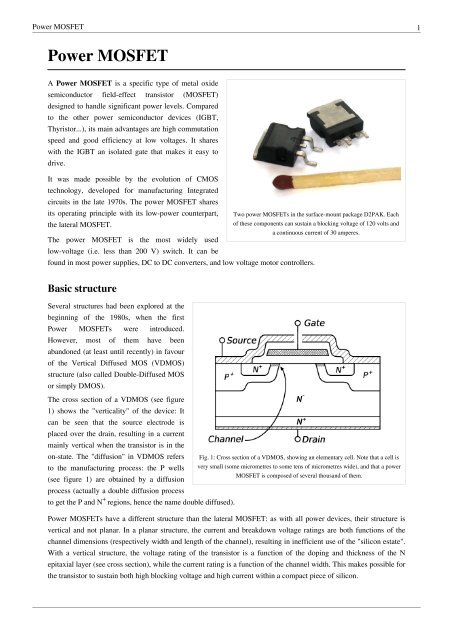
Power MOSFET
Power MOSFET
Power MOSFET

You also want an ePaper? Increase the reach of your titles
YUMPU automatically turns print PDFs into web optimized ePapers that Google loves.
<strong>Power</strong> <strong>MOSFET</strong> 1<strong>Power</strong> <strong>MOSFET</strong>A <strong>Power</strong> <strong>MOSFET</strong> is a specific type of metal oxidesemiconductor field-effect transistor (<strong>MOSFET</strong>)designed to handle significant power levels. Comparedto the other power semiconductor devices (IGBT,Thyristor...), its main advantages are high commutationspeed and good efficiency at low voltages. It shareswith the IGBT an isolated gate that makes it easy todrive.It was made possible by the evolution of CMOStechnology, developed for manufacturing Integratedcircuits in the late 1970s. The power <strong>MOSFET</strong> sharesits operating principle with its low-power counterpart, Two power <strong>MOSFET</strong>s in the surface-mount package D2PAK. Eachthe lateral <strong>MOSFET</strong>.of these components can sustain a blocking voltage of 120 volts anda continuous current of 30 amperes.The power <strong>MOSFET</strong> is the most widely usedlow-voltage (i.e. less than 200 V) switch. It can befound in most power supplies, DC to DC converters, and low voltage motor controllers.Basic structureSeveral structures had been explored at thebeginning of the 1980s, when the first<strong>Power</strong> <strong>MOSFET</strong>s were introduced.However, most of them have beenabandoned (at least until recently) in favourof the Vertical Diffused MOS (VDMOS)structure (also called Double-Diffused MOSor simply DMOS).The cross section of a VDMOS (see figure1) shows the "verticality" of the device: Itcan be seen that the source electrode isplaced over the drain, resulting in a currentmainly vertical when the transistor is in theon-state. The "diffusion" in VDMOS refers Fig. 1: Cross section of a VDMOS, showing an elementary cell. Note that a cell isto the manufacturing process: the P wells very small (some micrometres to some tens of micrometres wide), and that a power<strong>MOSFET</strong> is composed of several thousand of them.(see figure 1) are obtained by a diffusionprocess (actually a double diffusion processto get the P and N + regions, hence the name double diffused).<strong>Power</strong> <strong>MOSFET</strong>s have a different structure than the lateral <strong>MOSFET</strong>: as with all power devices, their structure isvertical and not planar. In a planar structure, the current and breakdown voltage ratings are both functions of thechannel dimensions (respectively width and length of the channel), resulting in inefficient use of the "silicon estate".With a vertical structure, the voltage rating of the transistor is a function of the doping and thickness of the Nepitaxial layer (see cross section), while the current rating is a function of the channel width. This makes possible forthe transistor to sustain both high blocking voltage and high current within a compact piece of silicon.
<strong>Power</strong> <strong>MOSFET</strong> 2It is worth noting that power <strong>MOSFET</strong>s with lateral structure exist. They are mainly used in high-end audioamplifiers. Their advantage is a better behaviour in the saturated region (corresponding to the linear region of abipolar transistor) than the vertical <strong>MOSFET</strong>s. Vertical <strong>MOSFET</strong>s are designed for switching applications, so theyare only used in On or Off states.On-state resistanceWhen the power <strong>MOSFET</strong> is in the on-state (see <strong>MOSFET</strong> for adiscussion on operation modes), it exhibits a resistive behaviourbetween the drain and source terminals. It can be seen in figure 2that this resistance (called R DSonfor "drain to source resistance inon-state") is the sum of many elementary contributions:• R Sis the source resistance. It represents all resistances betweenthe source terminal of the package to the channel of the<strong>MOSFET</strong>: resistance of the wire bonds, of the sourcemetallisation, and of the N + wells;• R ch. This is the channel resistance. It is inversely proportionalto the channel width, and for a given die size, to the channeldensity. The channel resistance is one of the main contributorsto the R DSonof low-voltage <strong>MOSFET</strong>s, and intensive work hasFig.2: Contribution of the different parts of the<strong>MOSFET</strong> to the on-state resistance.been carried out to reduce their cell size in order to increase the channel density;• R ais the access resistance. It represents the resistance of the epitaxial zone directly under the gate electrode,where the direction of the current changes from horizontal (in the channel) to vertical (to the drain contact);• R JFETis the detrimental effect of the cell size reduction mentioned above: the P implantations (see figure 1) formthe gates of a parasitic JFET transistor that tend to reduce the width of the current flow;• R nis the resistance of the epitaxial layer. As the role of this layer is to sustain the blocking voltage, R nis directlyrelated to the voltage rating of the device. A high voltage <strong>MOSFET</strong> requires a thick, low-doped layer (i.e. highlyresistive), whereas a low-voltage transistor only requires a thin layer with a higher doping level (i.e. lessresistive). As a result, R nis the main factor responsible for the resistance of high-voltage <strong>MOSFET</strong>s;• R Dis the equivalent of R Sfor the drain. It represents the resistance of the transistor substrate (note that the crosssection in figure 1 is not at scale, the bottom N + layer is actually the thickest) and of the package connections.
<strong>Power</strong> <strong>MOSFET</strong> 3Breakdown voltage/on-state resistance trade-offWhen in the OFF-state, the power <strong>MOSFET</strong>is equivalent to a PIN diode (constituted bythe P + diffusion, the N - epitaxial layer andthe N + substrate). When this highlynon-symmetrical structure is reverse-biased,the space-charge region extends principallyon the light-doped side, i.e. over the N -layer. This means that this layer has towithstand most of the <strong>MOSFET</strong>'s OFF-statedrain-to-source voltage.However, when the <strong>MOSFET</strong> is in theON-state, this N - layer has no function.Furthermore, as it is a lightly doped region,its intrinsic resistivity is non-negligible andadds to the <strong>MOSFET</strong>'s ON-stateDrain-to-Source Resistance (R DSon) (this is the R nresistance in figure 2).Fig. 3: The R DSonof the <strong>MOSFET</strong>s increase with their Voltage rating.Two main parameters govern both the breakdown voltage and the R DSonof the transistor: the doping level and thethickness of the N - epitaxial layer. The thicker the layer and the lower its doping level, the higher the breakdownvoltage. On the contrary, the thinner the layer and the higher the doping level, the lower the R DSon(and therefore thelower the conduction losses of the <strong>MOSFET</strong>). Therefore, it can be seen that there is a trade-off in the design of a<strong>MOSFET</strong>, between its voltage rating and its ON-state resistance. This is demonstrated by the plot in figure 3.Body diodeIt can be seen in figure 1 that the source metallization connects both the N + and P implantations, although theoperating principle of the <strong>MOSFET</strong> only requires the source to be connected to the N + zone. However, if it were, thiswould result in a floating P zone between the N-doped source and drain, which is equivalent to a NPN transistor witha non-connected base. Under certain conditions (under high drain current, when the on-state drain to source voltageis in the order of some volts), this parasitic NPN transistor would be triggered, making the <strong>MOSFET</strong> uncontrollable.The connection of the P implantation to the source metallization shorts the base of the parasitic transistor to itsemitter (the source of the <strong>MOSFET</strong>) and thus prevents spurious latching.This solution, however, creates a diode between the drain (cathode) and the source (anode) of the <strong>MOSFET</strong>, makingit able to block current in only one direction.
<strong>Power</strong> <strong>MOSFET</strong> 4Switching operationBecause of their unipolar nature, the power <strong>MOSFET</strong> can switchat very high speed. Indeed, there is no need to remove minoritycarriers as with bipolar devices.The only intrinsic limitation in commutation speed is due to theinternal capacitances of the <strong>MOSFET</strong> (see figure 4). Thesecapacitances must be charged or discharged when the transistorswitches. This can be a relatively slow process because the currentthat flows through the gate capacitances is limited by the externaldriver circuit. This circuit will actually dictate the commutationspeed of the transistor (assuming the power circuit has sufficientlylow inductance).CapacitancesIn the <strong>MOSFET</strong>s datasheets, the capacitances are often named C iss(input capacitance, drain and source terminal shorted), C oss(outputFig. 4: Location of the intrinsic capacitances of apower <strong>MOSFET</strong>.capacitance, gate and source shorted), and C rss(reverse transfer capacitance, gate and source shorted). Therelationship between these capacitances and those described below is:Where C GS, C GDand C DSare respectively the gate-to-source, gate-to-drain and drain-to-source capacitances (seebelow). Manufacturers prefer to quote C iss, C ossand C rssbecause they can be directly measured on the transistor.However, as C GS, C GDand C DSare closer to the physical meaning, they will be used in the remaining of this article.Gate to source capacitanceThe C GScapacitance is constituted by the parallel connection of C oxN+, C oxPand C oxm(see figure 4). As the N + andP regions are highly doped, the two former capacitances can be considered as constant. C oxmis the capacitancebetween the (polysilicon) gate and the (metal) source electrode, so it is also constant. Therefore, it is commonpractice to consider C GSas a constant capacitance, i.e. its value does not depend on the transistor state.Gate to drain capacitanceThe C GDcapacitance can be seen as the connection in series of two elementary capacitances. The first one is theoxide capacitance (C oxD), constituted by the gate electrode, the silicon dioxide and the top of the N epitaxial layer. Ithas a constant value. The second capacitance (C CDj) is caused by the extension of the space-charge zone when the<strong>MOSFET</strong> is in off-state (see the section Blocking Voltage). Therefore, it is dependent upon the drain to sourcevoltage. From this, the value of C GDis:The width of the space-charge region is given by [1]where is the permittivity of the Silicon, q is the electron charge, and N is the doping level. The value of C GDjcan be approximated using the expression of the plane capacitor:
<strong>Power</strong> <strong>MOSFET</strong> 5Where A GDis the surface area of the gate-drain overlap. Therefore, it comes:It can be seen that C GDj(and thus C GD) is a capacitance which value is dependent upon the gate to drain voltage. Asthis voltage increases, the capacitance decreases. When the <strong>MOSFET</strong> is in on-state, C GDjis shunted, so the gate todrain capacitance remains equal to C oxD, a constant value.Drain to source capacitanceAs the source metallization overlaps the P-wells (see figure 1), the drain and source terminals are separated by a P-Njunction. Therefore, C DSis the junction capacitance. This is a non-linear capacitance, and its value can be calculatedusing the same equation as for C GDj.Other dynamic elementsPackaging inductancesTo operate, the <strong>MOSFET</strong> must be connected to theexternal circuit, most of the time using wire bonding(although alternative techniques are investigated).These connection exhibit a parasitic inductance, whichis in no way specific to the <strong>MOSFET</strong> technology, buthas important effects because of its high commutationspeed. Parasitic inductances tend to maintain theircurrent constant and generate overvoltage during thetransistor turn off, resulting in increasing commutationlosses.A parasitic inductance can be associated with eachterminal of the <strong>MOSFET</strong>. They have different effects:• the gate inductance has little influence (assuming itis lower than some hundreds of nanohenries),because the current gradients on the gate areEquivalent circuit of a power <strong>MOSFET</strong>, including the dynamicrelatively slow. In some cases, however, the gateelements (capacitors, inductors), the parasitic resistors, the bodyinductance and the input capacitance of thediode.transistor can constitute an oscillator. This must beavoided as it results in very high commutation losses (up to the destruction of the device). On a typical design,parasitic inductances are kept low enough to prevent this phenomenon;• the drain inductance tends to reduce the drain voltage when the <strong>MOSFET</strong> turns on, so it reduces turn on losses.However, as it creates an overvoltage during turn-off, it increases turn-off losses;• the source parasitic inductance has the same behaviour as the drain inductance, plus a feedback effect that makescommutation last longer, thus increasing commutation losses.• at the beginning of a fast turn-on, due to the source inductance, the voltage at the source (on the die) will beable to jump up as well as the gate voltage; the internal V GSvoltage will remain low for a longer time,therefore delaying turn-on.
<strong>Power</strong> <strong>MOSFET</strong> 6• at the beginning of a fast turn-off, as current through the source inductance decreases sharply, the resultingvoltage across it goes negative (with respect to the lead outside the package) raising the internal V GSvoltage,keeping the <strong>MOSFET</strong> on, and therefore delaying turn-off.Limits of operationGate oxide breakdownThe gate oxide is very thin (100 nm or less), so it can only sustain a limited voltage. In the datasheets, manufacturersoften state a maximum gate to source voltage, around 20 V, and exceeding this limit can result in destruction of thecomponent. Furthermore, a high gate to source voltage reduces significantly the lifetime of the <strong>MOSFET</strong>, with littleto no advantage on R DSonreduction.Maximum drain to source voltage<strong>Power</strong> <strong>MOSFET</strong>s have a maximum specified drain to source voltage, beyond which breakdown may occur.Exceeding the breakdown voltage causes the device to conduct, potentially damaging it and other circuit elementsdue to excessive power dissipation.Maximum drain currentThe drain current must generally stay below a certain specified value (maximum continuous drain current). It canreach higher values for very short durations of time (maximum pulsed drain current, sometimes specified for variouspulse durations). The drain current is limited by heating due to resistive losses in internal components such as bondwires, and other phenomena such as electromigration in the metal layer.Maximum temperatureThe junction temperature (T J) of the <strong>MOSFET</strong> must stay under a specified maximum value for the device to functionreliably, determined by <strong>MOSFET</strong> die layout and packaging materials. The packaging often limits the maximumjunction temperature, due to the molding compound and (where used) epoxy characteristics.The maximum operating ambient temperature is determined by the power dissipation and thermal resistance. Thejunction-to-case thermal resistance is intrinsic to the device and package; the case-to-ambient thermal resistance islargely dependent on the board/mounting layout, heatsinking area and air/fluid flow.The type of power dissipation, whether continuous or pulsed, affects the maximum operating temperature, due tothermal capacitance characteristics; in general, the lower the frequency of pulses for a given power dissipation, thehigher maximum operating ambient temperature, due to allowing a longer interval for the device to cool down.Models, such as a Foster Network, can be used to analyze temperature dynamics from power transients.Safe operating areaThe safe operating area defines the combined ranges of drain current and drain to source voltage the power <strong>MOSFET</strong>is able to handle without damage. It is represented graphically as an area in the plane defined by these twoparameters. Both drain current and drain to source voltage must stay below their respective maximum values, buttheir product must also stay below the maximum power dissipation the device is able to handle. Thus the devicecannot be operated at both its specified maximum drain current and maximum drain to source voltage. [2]
<strong>Power</strong> <strong>MOSFET</strong> 7Latch-up (LU)The equivalent circuit for a <strong>MOSFET</strong> consist of one <strong>MOSFET</strong> in parallel with a parasitic BJT (Bipolar JunctionTransistor). If the BJT turns ON, it cannot be turned off since the gate has no control over it. This phenomenon isknown as 'latch-up', which can lead to device destruction. The BJT can be turned on due to a voltage drop across thep-type body region. To avoid latch-up, the body and the source are typically short circuited within the devicepackage.TechnologyLayoutCellular structureAs described above, the current handling capability of a power<strong>MOSFET</strong> is determined by its gate channel width. The gatechannel width is the third (Z-axis) dimension of the cross-sectionspictured.To minimize cost and size, it is valuable to keep the transistor's diearea size as small as possible. Therefore, optimizations have beendeveloped to increase the width of the channel surface area (i.e.increase the "channel density"). They mainly consist of creatingcellular structures repeated over the whole area of the <strong>MOSFET</strong>die. Several shapes have been proposed for these cells, the mostfamous being the International Rectifier's "Hexfet" (hexagonalshape).This <strong>Power</strong> <strong>MOSFET</strong> has a meshed gate, with squarecellsAnother way to increase the channel density is to reduce the sizeof the elementary structure. This allows for more cells in a givensurface area, and therefore more channel width. However, as thecell size shrinks, it becomes more difficult to ensure proper contactof every cell. To overcome this, a "strip" structure is often used(see figure). It is less efficient than a cellular structure ofequivalent resolution in terms of channel density, but can copewith smaller pitch.StructuresThe gate layout of this <strong>MOSFET</strong> is constituted ofparallel stripes.P-substrate power <strong>MOSFET</strong>A P-substrate <strong>MOSFET</strong> (often referred to as PMOS) is a <strong>MOSFET</strong> with opposite doping types (N instead of P and Pinstead of N in the cross-section in figure 1). This <strong>MOSFET</strong> is made using a P-type substrate, with a P - epitaxy. Asthe channel sits in a N-region, this transistor is turned on by a negative gate to source voltage. This makes it desirablein a buck converter, where one of the terminals of the switch is connected to the high side of the input voltage: with aN-<strong>MOSFET</strong>, this configuration requires to apply to the gate a voltage equal to, whereas no voltageover is required with a P-<strong>MOSFET</strong>.The main disadvantage of this type of <strong>MOSFET</strong> is the poor on-state performance: it uses holes as charge carriers,which have a much lower mobility than electrons. As resistivity is directly related to mobility, a given PMOS will
<strong>Power</strong> <strong>MOSFET</strong> 8have athree times higher than a N-<strong>MOSFET</strong> with the same dimensions.VMOSThis structure has a V-groove at the gate region andwas used for the first commercial devices [3] .The VMOS structure has a V-groove at the gate regionUMOS (also called Trench-MOS)In this <strong>Power</strong> <strong>MOSFET</strong> structure, the gate electrode isburied in a trench etched in the silicon. This results in avertical channel. The main interest of the structure isthe absence of the JFET effect. The name of thestructure comes from the U-shape of the trench.CoolMOSEspecially for voltages beyond 500 V somemanufacturers, most notably Infineon Technologies,have begun to use a charge compensation principle.Thus the resistance in the epitaxial layer as biggestcontributor in high voltage <strong>MOSFET</strong>s can be reducedby a factor >5.The UMOS has a trench gate. It is intended to increase the channeldensity by making the channel vertical
<strong>Power</strong> <strong>MOSFET</strong> 9Notes[1] S. M. Sze Modern semiconductor device physics John Wiley and Sons, Inc 1998 ISBN 0-471-15237-4[2] Pierre Aloïsi, Les transistors MOS de puissance in Interrupteurs électroniques de puissance, traite EGEM, under the direction of RobertPerret, Lavoisier, Paris, 2003 [in French] ISBN 2-7462-0671-4[3] Duncan A. Grant, John Gowar POWER <strong>MOSFET</strong>S: Theory and Applications John Wiley and Sons, Inc ISBN 0-471-82867-X , 1989References• "<strong>Power</strong> Semiconductor Devices", B. Jayant Baliga, PWS publishing Company, Boston. ISBN 0-534-94098-6
Article Sources and Contributors 10Article Sources and Contributors<strong>Power</strong> <strong>MOSFET</strong> Source: http://en.wikipedia.org/w/index.php?oldid=424590719 Contributors: Aagibby7, Adamrice, Appraiser, Archimerged, Babui, Bobblewik, Chris the speller, Congruence,CyrilB, David Haslam, DavideAndrea, Dicklyon, Dv82matt, Eugene van der Pijll, Foobaz, Gbmaizol, Glenn, Hairy Dude, Hankwang, Hooperbloob, Humatronic, Jcmaco, Lowenthalm, Malinov,Manavbhardwaj, Mboverload, Mcris31, Mild Bill Hiccup, Mindmatrix, Moogle10000, Mortense, Mortivik, Naomechateies, Nazli, Nickmn, PlantTrees, Razvan784, Rogerbrent, Seidenstud,Tellyaddict, ThePianoMan, TwelveBaud, Weedwhacker128, Woohookitty, Wtshymanski, ^musaz, 71 anonymous editsImage Sources, Licenses and ContributorsImage:D2PAK.JPG Source: http://en.wikipedia.org/w/index.php?title=File:D2PAK.JPG License: Creative Commons Attribution-Sharealike 2.5 Contributors: CyrilB, Geofrog, Inductiveload,Tothwolf, 1 anonymous editsImage:Vdmos_cross_section_en.svg Source: http://en.wikipedia.org/w/index.php?title=File:Vdmos_cross_section_en.svg License: Creative Commons Attribution-Sharealike 2.5 Contributors:Cepheiden, CyrilB, WikipediaMasterImage:Mosfet_resistances.svg Source: http://en.wikipedia.org/w/index.php?title=File:Mosfet_resistances.svg License: Creative Commons Attribution-Sharealike 2.5 Contributors: CyrilB,WikipediaMasterimage:Bv_rdson.png Source: http://en.wikipedia.org/w/index.php?title=File:Bv_rdson.png License: Creative Commons Attribution-Sharealike 2.5 Contributors: CyrilB, EnEdC,WikipediaMasterImage:Mosfet_capacitances.svg Source: http://en.wikipedia.org/w/index.php?title=File:Mosfet_capacitances.svg License: Creative Commons Attribution-Sharealike 2.5 Contributors:Cepheiden, CyrilB, WikipediaMasterImage:Mosfet_equivalent_circuit.svg Source: http://en.wikipedia.org/w/index.php?title=File:Mosfet_equivalent_circuit.svg License: Creative Commons Attribution-Sharealike 2.5Contributors: Cepheiden, CyrilB, D-Kuru, WikipediaMasterimage:<strong>Power</strong>_mos_cell_layout.svg Source: http://en.wikipedia.org/w/index.php?title=File:<strong>Power</strong>_mos_cell_layout.svg License: GNU Free Documentation License Contributors: CyrilBUTTAYimage:<strong>Power</strong>_mos_strip_layout.svg Source: http://en.wikipedia.org/w/index.php?title=File:<strong>Power</strong>_mos_strip_layout.svg License: GNU Free Documentation License Contributors: CyrilBUTTAYImage:VMOS_cross_section_en.png Source: http://en.wikipedia.org/w/index.php?title=File:VMOS_cross_section_en.png License: Public Domain Contributors: User:Babuiimage:Umos_cross_section_en.svg Source: http://en.wikipedia.org/w/index.php?title=File:Umos_cross_section_en.svg License: Creative Commons Attribution-Sharealike 2.5 Contributors:Cyril BUTTAYLicenseCreative Commons Attribution-Share Alike 3.0 Unportedhttp:/ / creativecommons. org/ licenses/ by-sa/ 3. 0/