BPW17N Silicon NPN Phototransistor - Vishay
BPW17N Silicon NPN Phototransistor - Vishay BPW17N Silicon NPN Phototransistor - Vishay
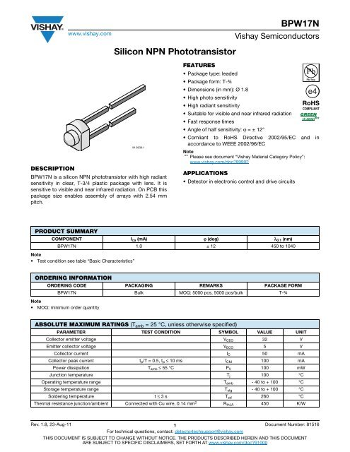
www.vishay.comBPW17NVishay SemiconductorsSilicon NPN PhototransistorDESCRIPTION94 8638-1BPW17N is a silicon NPN phototransistor with high radiantsensitivity in clear, T-3/4 plastic package with lens. It issensitive to visible and near infrared radiation. On PCB thispackage size enables assembly of arrays with 2.54 mmpitch.FEATURES• Package type: leaded• Package form: T-¾• Dimensions (in mm): Ø 1.8• High photo sensitivity• High radiant sensitivity• Suitable for visible and near infrared radiation• Fast response times• Angle of half sensitivity: ϕ = ± 12°• Comliant to RoHS Directive 2002/95/EC and inaccordance to WEEE 2002/96/ECNote** Please see document “Vishay Material Category Policy”:www.vishay.com/doc?99902APPLICATIONS• Detector in electronic control and drive circuitsPRODUCT SUMMARYCOMPONENT I ca (mA) ϕ (deg) λ 0.1 (nm)BPW17N 1.0 ± 12 450 to 1040Note• Test condition see table “Basic Characteristics”ORDERING INFORMATIONORDERING CODE PACKAGING REMARKS PACKAGE FORMBPW17N Bulk MOQ: 5000 pcs, 5000 pcs/bulk T-¾Note• MOQ: minimum order quantityABSOLUTE MAXIMUM RATINGS (T amb = 25 °C, unless otherwise specified)PARAMETER TEST CONDITION SYMBOL VALUE UNITCollector emitter voltage V CEO 32 VEmitter collector voltage V ECO 5 VCollector current I C 50 mACollector peak current t p /T = 0.5, t p ≤ 10 ms I CM 100 mAPower dissipation T amb ≤ 55 °C P V 100 mWJunction temperature T j 100 °COperating temperature range T amb - 40 to + 100 °CStorage temperature range T stg - 40 to + 100 °CSoldering temperature t ≤ 3 s T sd 260 °CThermal resistance junction/ambient Connected with Cu wire, 0.14 mm 2 R thJA 450 K/WRev. 1.8, 23-Aug-11 1 Document Number: 81516For technical questions, contact: detectortechsupport@vishay.comTHIS DOCUMENT IS SUBJECT TO CHANGE WITHOUT NOTICE. THE PRODUCTS DESCRIBED HEREIN AND THIS DOCUMENTARE SUBJECT TO SPECIFIC DISCLAIMERS, SET FORTH AT www.vishay.com/doc?91000
- Page 2 and 3: www.vishay.comBPW17NVishay Semicond
- Page 4 and 5: www.vishay.comBPW17NVishay Semicond
www.vishay.com<strong>BPW17N</strong><strong>Vishay</strong> Semiconductors<strong>Silicon</strong> <strong>NPN</strong> <strong>Phototransistor</strong>DESCRIPTION94 8638-1<strong>BPW17N</strong> is a silicon <strong>NPN</strong> phototransistor with high radiantsensitivity in clear, T-3/4 plastic package with lens. It issensitive to visible and near infrared radiation. On PCB thispackage size enables assembly of arrays with 2.54 mmpitch.FEATURES• Package type: leaded• Package form: T-¾• Dimensions (in mm): Ø 1.8• High photo sensitivity• High radiant sensitivity• Suitable for visible and near infrared radiation• Fast response times• Angle of half sensitivity: ϕ = ± 12°• Comliant to RoHS Directive 2002/95/EC and inaccordance to WEEE 2002/96/ECNote** Please see document “<strong>Vishay</strong> Material Category Policy”:www.vishay.com/doc?99902APPLICATIONS• Detector in electronic control and drive circuitsPRODUCT SUMMARYCOMPONENT I ca (mA) ϕ (deg) λ 0.1 (nm)<strong>BPW17N</strong> 1.0 ± 12 450 to 1040Note• Test condition see table “Basic Characteristics”ORDERING INFORMATIONORDERING CODE PACKAGING REMARKS PACKAGE FORM<strong>BPW17N</strong> Bulk MOQ: 5000 pcs, 5000 pcs/bulk T-¾Note• MOQ: minimum order quantityABSOLUTE MAXIMUM RATINGS (T amb = 25 °C, unless otherwise specified)PARAMETER TEST CONDITION SYMBOL VALUE UNITCollector emitter voltage V CEO 32 VEmitter collector voltage V ECO 5 VCollector current I C 50 mACollector peak current t p /T = 0.5, t p ≤ 10 ms I CM 100 mAPower dissipation T amb ≤ 55 °C P V 100 mWJunction temperature T j 100 °COperating temperature range T amb - 40 to + 100 °CStorage temperature range T stg - 40 to + 100 °CSoldering temperature t ≤ 3 s T sd 260 °CThermal resistance junction/ambient Connected with Cu wire, 0.14 mm 2 R thJA 450 K/WRev. 1.8, 23-Aug-11 1 Document Number: 81516For technical questions, contact: detectortechsupport@vishay.comTHIS DOCUMENT IS SUBJECT TO CHANGE WITHOUT NOTICE. THE PRODUCTS DESCRIBED HEREIN AND THIS DOCUMENTARE SUBJECT TO SPECIFIC DISCLAIMERS, SET FORTH AT www.vishay.com/doc?91000
www.vishay.com<strong>BPW17N</strong><strong>Vishay</strong> Semiconductors125P V- Power Dissipation (mW)100755025R thJA= 450 K/W00 20 40 60 8094 8308 T amb- Ambient Temperature (°C)100Fig. 1 - Power Dissipation Limit vs. Ambient TemperatureBASIC CHARACTERISTICS (T amb = 25 °C, unless otherwise specified)PARAMETER TEST CONDITION SYMBOL MIN. TYP. MAX. UNITCollector emitter breakdown voltage I C = 1 mA V (BR)CEO 32 VCollector emitter dark current V CE = 20 V, E = 0 I CEO 1 200 nACollector emitter capacitance V CE = 5 V, f = 1 MHz, E = 0 C CEO 8 pFCollector light currentE e = 1 mW/cm 2 , λ = 950 nm,V CE = 5 VI ca 0.5 1.0 mAAngle of half sensitivity ϕ ± 12 degWavelength of peak sensitivity λ p 825 nmRange of spectral bandwidth λ 0.1 450 to 1040 nmCollector emitter saturation voltageE e = 1 mW/cm 2 , λ = 950 nm,I C = 0.1 mAV CEsat 0.3 VTurn-on time V S = 5 V, I C = 5 mA, R L = 100 Ω t on 4.8 μsTurn-off time V S = 5 V, I C = 5 mA, R L = 100 Ω t off 5.0 μsCut-off frequency V S = 5 V, I C = 5 mA, R L = 100 Ω f c 120 kHzBASIC CHARACTERISTICS (T amb = 25 °C, unless otherwise specified)I CEO- Collector Dark Current (nA)10 410 3V CE= 20 V10 210 1I ca rel - Relative Collector Current1.81.61.41.21.00.8V CE = 5 VE e = 1 mW/cm 2λ = 950 nm2.010 094 82352040 60 80T amb- Ambient Temperature (°C)1000.60 20 40 60 80 10094 8239 T amb - Ambient Temperature (°C)Fig. 1 - Collector Dark Current vs. Ambient Temperature Fig. 2 - Relative Collector Current vs. Ambient TemperatureRev. 1.8, 23-Aug-11 2 Document Number: 81516For technical questions, contact: detectortechsupport@vishay.comTHIS DOCUMENT IS SUBJECT TO CHANGE WITHOUT NOTICE. THE PRODUCTS DESCRIBED HEREIN AND THIS DOCUMENTARE SUBJECT TO SPECIFIC DISCLAIMERS, SET FORTH AT www.vishay.com/doc?91000
www.vishay.com<strong>BPW17N</strong><strong>Vishay</strong> Semiconductors1012I ca - Collector Light Current (mA)94 831310.10.01V CE =5Vλ = 950 nm0.0010.01 0.1 1E e - Irradiance (mW/cm 2 )10t on /toff-Turn on / Turn off Time (µs)94 8238108642V CE =5VR L = 100 Ωλ = 950 nmt offt on00 4 8 12I C - Collector Current (mA)16Fig. 3 - Collector Light Current vs. IrradianceFig. 6 - Turn-on/Turn-off Time vs. Collector CurrentI ca - Collector Light Current (mA)94 8242101λ = 950 nm0.10.1 1 10E e = 1 mW/cm 20.5 mW/cm 20.2 mW/cm 2V CE - Collector Emitter Voltage (V)100Fig. 4 - Collector Light Current vs. Collector Emitter VoltageS(λ) - Relative Spectral Sensitivityrel1.00.80.60.40.20400 600 800 100094 8241λ -Wavelength (nm)Fig. 7 - Relative Spectral Sensitivity vs. WavelengthC CEO- Collector Emitter Capacitance (pF)20161294 824084f = 1 MHz00.1 1 10V CE- Collector Emitter Voltage (V)100Fig. 5 - Collector Emitter Capacitance vs. Collector Emitter VoltageS rel- Relative Radiant Sensitivity0° 10° 20°30°40°1.00.90.80.750°60°70°80°0.6 0.4 0.2 094 8243Fig. 8 - Relative Radiant Sensitivity vs. Angular Displacementϕ - Angular DisplacementRev. 1.8, 23-Aug-11 3 Document Number: 81516For technical questions, contact: detectortechsupport@vishay.comTHIS DOCUMENT IS SUBJECT TO CHANGE WITHOUT NOTICE. THE PRODUCTS DESCRIBED HEREIN AND THIS DOCUMENTARE SUBJECT TO SPECIFIC DISCLAIMERS, SET FORTH AT www.vishay.com/doc?91000
www.vishay.com<strong>BPW17N</strong><strong>Vishay</strong> SemiconductorsPACKAGE DIMENSIONS in millimeters± 0.15R 1.65EC3.3 ± 0.15Chip position± 0.32.9± 0.11.55(2)1.8 ± 0.1± 0.529.8± 0.33.42.4Area not plane± 0.250.4+ 0.150.5+ 0.2- 0.12.54 nom.1.5technical drawingsaccording to DINspecifications6.544-5042.01-4Issue:1; 01.07.9696 12187Rev. 1.8, 23-Aug-11 4 Document Number: 81516For technical questions, contact: detectortechsupport@vishay.comTHIS DOCUMENT IS SUBJECT TO CHANGE WITHOUT NOTICE. THE PRODUCTS DESCRIBED HEREIN AND THIS DOCUMENTARE SUBJECT TO SPECIFIC DISCLAIMERS, SET FORTH AT www.vishay.com/doc?91000
www.vishay.comLegal Disclaimer Notice<strong>Vishay</strong>DisclaimerALL PRODUCT, PRODUCT SPECIFICATIONS AND DATA ARE SUBJECT TO CHANGE WITHOUT NOTICE TO IMPROVERELIABILITY, FUNCTION OR DESIGN OR OTHERWISE.<strong>Vishay</strong> Intertechnology, Inc., its affiliates, agents, and employees, and all persons acting on its or their behalf (collectively,“<strong>Vishay</strong>”), disclaim any and all liability for any errors, inaccuracies or incompleteness contained in any datasheet or in any otherdisclosure relating to any product.<strong>Vishay</strong> makes no warranty, representation or guarantee regarding the suitability of the products for any particular purpose orthe continuing production of any product. To the maximum extent permitted by applicable law, <strong>Vishay</strong> disclaims (i) any and allliability arising out of the application or use of any product, (ii) any and all liability, including without limitation special,consequential or incidental damages, and (iii) any and all implied warranties, including warranties of fitness for particularpurpose, non-infringement and merchantability.Statements regarding the suitability of products for certain types of applications are based on <strong>Vishay</strong>’s knowledge of typicalrequirements that are often placed on <strong>Vishay</strong> products in generic applications. Such statements are not binding statementsabout the suitability of products for a particular application. It is the customer’s responsibility to validate that a particularproduct with the properties described in the product specification is suitable for use in a particular application. Parametersprovided in datasheets and/or specifications may vary in different applications and performance may vary over time. Alloperating parameters, including typical parameters, must be validated for each customer application by the customer’stechnical experts. Product specifications do not expand or otherwise modify <strong>Vishay</strong>’s terms and conditions of purchase,including but not limited to the warranty expressed therein.Except as expressly indicated in writing, <strong>Vishay</strong> products are not designed for use in medical, life-saving, or life-sustainingapplications or for any other application in which the failure of the <strong>Vishay</strong> product could result in personal injury or death.Customers using or selling <strong>Vishay</strong> products not expressly indicated for use in such applications do so at their own risk. Pleasecontact authorized <strong>Vishay</strong> personnel to obtain written terms and conditions regarding products designed for such applications.No license, express or implied, by estoppel or otherwise, to any intellectual property rights is granted by this document or byany conduct of <strong>Vishay</strong>. Product names and markings noted herein may be trademarks of their respective owners.Material Category Policy<strong>Vishay</strong> Intertechnology, Inc. hereby certifies that all its products that are identified as RoHS-Compliant fulfill thedefinitions and restrictions defined under Directive 2011/65/EU of The European Parliament and of the Councilof June 8, 2011 on the restriction of the use of certain hazardous substances in electrical and electronic equipment(EEE) - recast, unless otherwise specified as non-compliant.Please note that some <strong>Vishay</strong> documentation may still make reference to RoHS Directive 2002/95/EC. We confirm thatall the products identified as being compliant to Directive 2002/95/EC conform to Directive 2011/65/EU.<strong>Vishay</strong> Intertechnology, Inc. hereby certifies that all its products that are identified as Halogen-Free follow Halogen-Freerequirements as per JEDEC JS709A standards. Please note that some <strong>Vishay</strong> documentation may still make referenceto the IEC 61249-2-21 definition. We confirm that all the products identified as being compliant to IEC 61249-2-21conform to JEDEC JS709A standards.Revision: 02-Oct-12 1 Document Number: 91000


