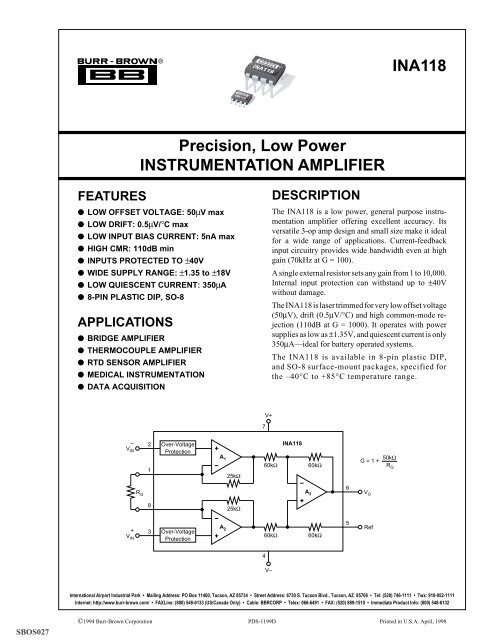
Precision, Low Power Instrumentation Amplifier
Precision, Low Power Instrumentation Amplifier
Precision, Low Power Instrumentation Amplifier

You also want an ePaper? Increase the reach of your titles
YUMPU automatically turns print PDFs into web optimized ePapers that Google loves.
TYPICAL PERFORMANCE CURVES (CONT)At T A = +25°C, V S = ±15V, unless otherwise noted.160POSITIVE POWER SUPPLY REJECTIONvs FREQUENCY160NEGATIVE POWER SUPPLY REJECTIONvs FREQUENCY<strong>Power</strong> Supply Rejection (dB)14012010080604020G = 1000G = 100G = 10G = 1<strong>Power</strong> Supply Rejection (dB)14012010080604020G = 1000G = 100G = 10G = 101 10 100 1k 10k 100kFrequency (Hz)010 100 1k 10k 100kFrequency (Hz)Input-Referred Noise Voltage (nV/√ Hz)1k100101INPUT- REFERRED NOISE VOLTAGEvs FREQUENCYFrequency (Hz)G = 1G = 10G = 100, 1000G = 1000 BW Limit1 10 1001kCurrent Noise(All Gains)1001010.110kInput Bias Current Noise (pA/√ Hz)Settling Time (µs)100010010SETTLING TIME vs GAINR L = 10kΩC L = 100pF1 10 100 1000Gain (V/V)0.01%0.1%Quiescent Current (µA)500400300QUIESCENT CURRENT and SLEW RATEvs TEMPERATURE2000–75 –50 –25 0 25 50 75 100 125Temperature (°C)Slew RateI QV S = ±15VV S = ±1.35V1.510.5Slew Rate (V/µs)Input Bias Current (mA)INPUT BIAS CURRENTvs INPUT OVERLOAD VOLTAGE108642G = 10000G = 1–2–4–6–8–10G = 1G = 1000–40 0 40Overload Voltage (V)5INA118®
TYPICAL PERFORMANCE CURVES (CONT)At T A = +25°C, V S = ±15V, unless otherwise noted.Offset Voltage Change (µV)OFFSET VOLTAGE vs WARM-UP TIME10864G = 100020–2–4–6–8–100 0.5 1.0 1.5 2.0 2.5 3.0Time from <strong>Power</strong> Supply Turn On (ms)Input Bias and Offset Current (nA)INPUT BIAS AND OFFSET CURRENTvs TEMPERATURE54I OS32±I b10–1–2–3–4–5–75 –50 –25 0 25 50 75 100 125Temperature (°C)Output Voltage Swing (V)V+(V+) –0.4(V+) –0.8(V–)+0.8(V–)+0.4OUTPUT VOLTAGE SWING vs OUTPUT CURRENTPositiveSingle <strong>Power</strong> Supply, V– = 0VGround-Referred LoadV S ≤ ±5VV S = ±15VNegativeV–0 1 2 3 4Output Current (mA)Output Voltage Swing (V)OUTPUT VOLTAGE SWINGvs POWER SUPPLY VOLTAGEV+(V+) –0.2Positive(V+) –0.4+85°C +25°C(V+) –0.6(V+) –0.8(V+) –1–40°CR L = 10kΩ(V–) +0.4+85°CNegative+25°C(V–) +0.2–40°CV–0 ±5 ±10 ±15 ±20<strong>Power</strong> Supply Voltage (V)16OUTPUT CURRENT LIMIT vs TEMPERATURE32MAXIMUM OUTPUT SWING vs FREQUENCYG = 10, 100Short Circuit Current (mA)1412108642–|I CL|+|I CL |Peak-to-Peak Output Voltage (V)282420161284G = 1G = 10000–75 –50 –25 0 25 50 75 100 125Temperature (°C)0100 1k 10k 100k 1MFrequency (Hz)®INA1186
TYPICAL PERFORMANCE CURVES (CONT)At T A = +25°C, V S = ±15V, unless otherwise noted.1THD + N vs FREQUENCYINPUT-REFERRED NOISE, 0.1Hz to 10HzG = 10THD + N (%)0.10.01R L = 10kΩ0.1µV/div(Noise Floor)R L = ∞0.00120 100 1k 10k 20kFrequency (Hz)1s/divSMALL-SIGNAL RESPONSESMALL-SIGNAL RESPONSEG = 1G = 10020mV/div20mV/divG = 10G = 100010µs/div100µs/divLARGE-SIGNAL RESPONSELARGE-SIGNAL RESPONSEG = 1G = 1005V/div5V/divG = 10G = 1000100µs/div100µs/div7INA118®
APPLICATION INFORMATIONFigure 1 shows the basic connections required for operationof the INA118. Applications with noisy or high impedancepower supplies may require decoupling capacitors close tothe device pins as shown.The output is referred to the output reference (Ref) terminalwhich is normally grounded. This must be a low-impedanceconnection to assure good common-mode rejection. A resistanceof 12Ω in series with the Ref pin will cause a typicaldevice to degrade to approximately 80dB CMR (G = 1).SETTING THE GAINGain of the INA118 is set by connecting a single externalresistor, R G , connected between pins 1 and 8:G = 1 + 50kΩR GCommonly used gains and resistor values are shown inFigure 1.The 50kΩ term in Equation 1 comes from the sum of the twointernal feedback resistors of A 1 and A 2 . These on-chipmetal film resistors are laser trimmed to accurate absolutevalues. The accuracy and temperature coefficient of theseresistors are included in the gain accuracy and drift specificationsof the INA118.(1)The stability and temperature drift of the external gainsetting resistor, R G , also affects gain. R G ’s contribution togain accuracy and drift can be directly inferred from the gainequation (1). <strong>Low</strong> resistor values required for high gain canmake wiring resistance important. Sockets add to the wiringresistance which will contribute additional gain error (possiblyan unstable gain error) in gains of approximately 100 orgreater.DYNAMIC PERFORMANCEThe typical performance curve “Gain vs Frequency” showsthat, despite its low quiescent current, the INA118 achieveswide bandwidth, even at high gain. This is due to thecurrent-feedback topology of the INA118. Settling time alsoremains excellent at high gain.The INA118 exhibits approximately 3dB peaking at 500kHzin unity gain. This is a result of its current-feedback topologyand is not an indication of instability. Unlike an op ampwith poor phase margin, the rise in response is a predictable+6dB/octave due to a response zero. A simple pole at300kHz or lower will produce a flat passband unity gainresponse.DESIRED R G NEAREST 1% R GGAIN (Ω) (Ω)1 NC NC2 50.00k 49.9k5 12.50k 12.4k10 5.556k 5.62k20 2.632k 2.61k50 1.02k 1.02k100 505.1 511200 251.3 249500 100.2 1001000 50.05 49.92000 25.01 24.95000 10.00 1010000 5.001 4.99V+0.1µF7– 2 Over-VoltageINA118V IN ProtectionA 160kΩ 60kΩ125kΩ6R G A 3825kΩ5A+23 Over-VoltageRefV IN60kΩ 60kΩProtection40.1µF+ –V O = G • (V IN – V IN )G = 1 + 50kΩR GLoad+V O–NC: No Connection.Also drawn in simplified form:V–V IN–R GINA118V OV IN+RefFIGURE 1. Basic Connections.®INA1188
SINGLE SUPPLY OPERATIONThe INA118 can be used on single power supplies of +2.7Vto +36V. Figure 5 shows a basic single supply circuit. Theoutput Ref terminal is connected to ground. Zero differentialinput voltage will demand an output voltage of 0V (ground).Actual output voltage swing is limited to approximately35mV above ground, when the load is referred to ground asshown. The typical performance curve “Output Voltage vsOutput Current” shows how the output voltage swing varieswith output current.+ –With single supply operation, V IN and V IN must both be0.98V above ground for linear operation. You cannot, forinstance, connect the inverting input to ground and measurea voltage connected to the non-inverting input.To illustrate the issues affecting low voltage operation,consider the circuit in Figure 5. It shows the INA118,operating from a single 3V supply. A resistor in series withthe low side of the bridge assures that the bridge outputvoltage is within the common-mode range of the amplifier’sinputs. Refer to the typical performance curve “Input Common-ModeRange vs Output Voltage” for 3V single supplyoperation.INPUT PROTECTIONThe inputs of the INA118 are individually protected forvoltages up to ±40V. For example, a condition of –40V onone input and +40V on the other input will not causedamage. Internal circuitry on each input provides low seriesimpedance under normal signal conditions. To provideequivalent protection, series input resistors would contributeexcessive noise. If the input is overloaded, the protectioncircuitry limits the input current to a safe value of approximately1.5 to 5mA. The typical performance curve “InputBias Current vs Input Overload Voltage” shows this inputcurrent limit behavior. The inputs are protected even if thepower supplies are disconnected or turned off.INSIDE THE INA118Figure 1 shows a simplified representation of the INA118.The more detailed diagram shown here provides additionalinsight into its operation.Each input is protected by two FET transistors thatprovide a low series resistance under normal signal conditions,preserving excellent noise performance. Whenexcessive voltage is applied, these transistors limit inputcurrent to approximately 1.5 to 5mA.The differential input voltage is buffered by Q 1 and Q 2and impressed across R G , causing a signal current to flowthrough R G , R 1 and R 2 . The output difference amp, A 3 ,removes the common-mode component of the input signaland refers the output signal to the Ref terminal.Equations in the figure describe the output voltages of A 1and A 2 . The V BE and IR drop across R 1 and R 2 produceoutput voltages on A 1 and A 2 that are approximately 1Vlower than the input voltages.A 1 Out = V CM – V BE – (10µA • 25kΩ) – V O /2A 2 Out = V CM – V BE – (10µA • 25kΩ) + V O /2Output Swing Range A 1 , A 2 ; (V+) – 0.65V to (V–) + 0.06V<strong>Amplifier</strong> Linear Input Range: (V+) – 0.65V to (V–) + 0.98VC 1 C 2V CM V D /210µA V B 10µAInput Bias CurrentA 1A 2Compensation60kΩ60kΩ–V INQ 1R 1R 2Q 225kΩ25kΩV D /2R G(External)+ –V O = G • (V IN – V IN )Output Swing Range:(V+) – 0.8V to (V–) + 0.35V60kΩA 360kΩV ORef+V INFIGURE 4. INA118 Simplified Circuit Diagram.®INA11810
+3V2V – ∆V3V10.0V6REF1022V+R 1R 2300Ω2V + ∆VR G INA118 V ORefPt1004150ΩR 1(1)KCuCuR GINA118V ONOTE: (1) R 1required to create proper common-mode voltage,only for low voltage operation — see text.FIGURE 5. Single-Supply Bridge <strong>Amplifier</strong>.–V IN+R GINA118V ORef RC 111MΩ0.1µFR 3100Ω = RTD at 0°CSEEBECKISACOEFFICIENTTYPE MATERIAL (µV/°C) R 1 , R 2E + Chromel 58.5 66.5kΩ– ConstantanJ + Iron 50.2 76.8kΩ– ConstantanK + Chromel 39.4 97.6kΩ– AlumelT + Copper 38.0 102kΩ– ConstantanFIGURE 7. Thermocouple <strong>Amplifier</strong> With Cold JunctionCompensation.RefOPA6021f –3dB=2πR 1C 1= 1.59Hz–V IN+R GINA118RefR 1I BI O =V INR 1• GFIGURE 6. AC-Coupled <strong>Instrumentation</strong> <strong>Amplifier</strong>.A 1I B ErrorA 1LoadI OOPA177OPA602OPA128±1.5nA±1pA±75fAFIGURE 8. Differential Voltage to Current Converter.2.8kΩRALAR G /2INA118V O2.8kΩRefG = 10RL390kΩ390kΩ1/2OPA260410kΩ1/2OPA2604FIGURE 9. ECG <strong>Amplifier</strong> With Right-Leg Drive.11INA118®
PACKAGE OPTION ADDENDUMwww.ti.com3-Oct-2003PACKAGING INFORMATIONORDERABLE DEVICE STATUS(1) PACKAGE TYPE PACKAGE DRAWING PINS PACKAGE QTYINA118P ACTIVE PDIP P 8 50INA118PB ACTIVE PDIP P 8 50INA118U ACTIVE SOIC D 8 100INA118U/2K5 ACTIVE SOIC D 8 2500INA118UB ACTIVE SOIC D 8 100INA118UB/2K5 ACTIVE SOIC D 8 2500(1) The marketing status values are defined as follows:ACTIVE: Product device recommended for new designs.LIFEBUY: TI has announced that the device will be discontinued, and a lifetime-buy period is in effect.NRND: Not recommended for new designs. Device is in production to support existing customers, but TI does not recommend using this part ina new design.PREVIEW: Device has been announced but is not in production. Samples may or may not be available.OBSOLETE: TI has discontinued the production of the device.
IMPORTANT NOTICETexas Instruments Incorporated and its subsidiaries (TI) reserve the right to make corrections, modifications,enhancements, improvements, and other changes to its products and services at any time and to discontinueany product or service without notice. Customers should obtain the latest relevant information before placingorders and should verify that such information is current and complete. All products are sold subject to TI’s termsand conditions of sale supplied at the time of order acknowledgment.TI warrants performance of its hardware products to the specifications applicable at the time of sale inaccordance with TI’s standard warranty. Testing and other quality control techniques are used to the extent TIdeems necessary to support this warranty. Except where mandated by government requirements, testing of allparameters of each product is not necessarily performed.TI assumes no liability for applications assistance or customer product design. Customers are responsible fortheir products and applications using TI components. To minimize the risks associated with customer productsand applications, customers should provide adequate design and operating safeguards.TI does not warrant or represent that any license, either express or implied, is granted under any TI patent right,copyright, mask work right, or other TI intellectual property right relating to any combination, machine, or processin which TI products or services are used. Information published by TI regarding third-party products or servicesdoes not constitute a license from TI to use such products or services or a warranty or endorsement thereof.Use of such information may require a license from a third party under the patents or other intellectual propertyof the third party, or a license from TI under the patents or other intellectual property of TI.Reproduction of information in TI data books or data sheets is permissible only if reproduction is withoutalteration and is accompanied by all associated warranties, conditions, limitations, and notices. Reproductionof this information with alteration is an unfair and deceptive business practice. TI is not responsible or liable forsuch altered documentation.Resale of TI products or services with statements different from or beyond the parameters stated by TI for thatproduct or service voids all express and any implied warranties for the associated TI product or service andis an unfair and deceptive business practice. TI is not responsible or liable for any such statements.Following are URLs where you can obtain information on other Texas Instruments products and applicationsolutions:ProductsApplications<strong>Amplifier</strong>s amplifier.ti.com Audio www.ti.com/audioData Converters dataconverter.ti.com Automotive www.ti.com/automotiveDSP dsp.ti.com Broadband www.ti.com/broadbandInterface interface.ti.com Digital Control www.ti.com/digitalcontrolLogic logic.ti.com Military www.ti.com/military<strong>Power</strong> Mgmt power.ti.com Optical Networking www.ti.com/opticalnetworkMicrocontrollers microcontroller.ti.com Security www.ti.com/securityTelephonywww.ti.com/telephonyVideo & Imaging www.ti.com/videoWirelesswww.ti.com/wirelessMailing Address:Texas InstrumentsPost Office Box 655303 Dallas, Texas 75265Copyright © 2003, Texas Instruments Incorporated