XAPP291: "Self-Addressing FIFO" - Xilinx
XAPP291: "Self-Addressing FIFO" - Xilinx XAPP291: "Self-Addressing FIFO" - Xilinx
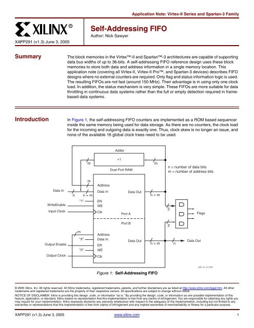
Application Note: Virtex-II Series and Spartan-3 FamilyXAPP291 (v1.3) June 3, 2005RSelf-Addressing FIFOAuthor: Nick SawyerSummaryThe block memories in the Virtex-II and Spartan-3 architectures are capable of supportingdata bus widths of up to 36-bits. A self-addressing FIFO reference design uses these blockmemories to store both data and address information in a single memory location. Thisapplication note (covering all Virtex-II, Virtex-II Pro, and Spartan-3 devices) describes FIFOdesigns where no external counters are required. Only flag and status information logic is used.The resulting FIFOs are not fast (around 150 MHz). Their advantage is in using only one clockload. In addition, the status mechanism is very simple. These FIFOs are more suitable for datathrottling in continuous data systems rather than the full or empty detection required in framebaseddata systems.IntroductionIn Figure 1, the self-addressing FIFO counters are implemented as a ROM based sequencerinside the same memory being used for data storage. As there are no counters, the clock loadfor the incoming and outgoing data is exactly one. Thus, clock skew is no longer an issue, andnone of the available 16 global clock trees need to be used.Adderm+1Dual Port RAMmn = number of data bitsm = number of address bitsmAddressData Innn + mData InData Outn + mWriteEnableInput Clock"1"ENWEClkPort A2FlagsPort B2Output Enablem"X""0"AddressData InENWEData Outn + mnData OutOutput ClockClkx291_01_011702Figure 1: Self-Addressing FIFO© 2005 Xilinx, Inc. All rights reserved. All Xilinx trademarks, registered trademarks, patents, and further disclaimers are as listed at http://www.xilinx.com/legal.htm. All othertrademarks and registered trademarks are the property of their respective owners. All specifications are subject to change without notice.NOTICE OF DISCLAIMER: Xilinx is providing this design, code, or information "as is." By providing the design, code, or information as one possible implementation of thisfeature, application, or standard, Xilinx makes no representation that this implementation is free from any claims of infringement. You are responsible for obtaining any rights youmay require for your implementation. Xilinx expressly disclaims any warranty whatsoever with respect to the adequacy of the implementation, including but not limited to anywarranties or representations that this implementation is free from claims of infringement and any implied warranties of merchantability or fitness for a particular purpose.XAPP291 (v1.3) June 3, 2005 www.xilinx.com 1
- Page 3 and 4: Implementing a Counter in a MemoryR
Application Note: Virtex-II Series and Spartan-3 Family<strong>XAPP291</strong> (v1.3) June 3, 2005R<strong>Self</strong>-<strong>Addressing</strong> FIFOAuthor: Nick SawyerSummaryThe block memories in the Virtex-II and Spartan-3 architectures are capable of supportingdata bus widths of up to 36-bits. A self-addressing FIFO reference design uses these blockmemories to store both data and address information in a single memory location. Thisapplication note (covering all Virtex-II, Virtex-II Pro, and Spartan-3 devices) describes FIFOdesigns where no external counters are required. Only flag and status information logic is used.The resulting FIFOs are not fast (around 150 MHz). Their advantage is in using only one clockload. In addition, the status mechanism is very simple. These FIFOs are more suitable for datathrottling in continuous data systems rather than the full or empty detection required in framebaseddata systems.IntroductionIn Figure 1, the self-addressing FIFO counters are implemented as a ROM based sequencerinside the same memory being used for data storage. As there are no counters, the clock loadfor the incoming and outgoing data is exactly one. Thus, clock skew is no longer an issue, andnone of the available 16 global clock trees need to be used.Adderm+1Dual Port RAMmn = number of data bitsm = number of address bitsmAddressData Innn + mData InData Outn + mWriteEnableInput Clock"1"ENWEClkPort A2FlagsPort B2Output Enablem"X""0"AddressData InENWEData Outn + mnData OutOutput ClockClkx291_01_011702Figure 1: <strong>Self</strong>-<strong>Addressing</strong> FIFO© 2005 <strong>Xilinx</strong>, Inc. All rights reserved. All <strong>Xilinx</strong> trademarks, registered trademarks, patents, and further disclaimers are as listed at http://www.xilinx.com/legal.htm. All othertrademarks and registered trademarks are the property of their respective owners. All specifications are subject to change without notice.NOTICE OF DISCLAIMER: <strong>Xilinx</strong> is providing this design, code, or information "as is." By providing the design, code, or information as one possible implementation of thisfeature, application, or standard, <strong>Xilinx</strong> makes no representation that this implementation is free from any claims of infringement. You are responsible for obtaining any rights youmay require for your implementation. <strong>Xilinx</strong> expressly disclaims any warranty whatsoever with respect to the adequacy of the implementation, including but not limited to anywarranties or representations that this implementation is free from claims of infringement and any implied warranties of merchantability or fitness for a particular purpose.<strong>XAPP291</strong> (v1.3) June 3, 2005 www.xilinx.com 1
Implementing a Counter in a MemoryRIn Figure 1, an example data transfer is started by writing data (23) to location x00. After theclock edge, the data output of port A contains x0123. The lower data byte (23) is ignored, theupper byte (x01) is fed back as the address for the next write. A one is added to x01 formerging with the next incoming data. For example, if the next incoming data is 45, then x0245is written into location x01. This value then appears at the output of port A. The next cycle willwrite to location x03 and so forth.Reading data is less complicated. An output clock and optional output enable signal are appliedto Port B. Data is read synchronous to the clock. The lower byte is the valid data that waswritten into Port A of the FIFO. The upper byte contains the address for the next read. Theupper byte is therefore fed back to the address inputs of Port B.Having covered the basic FIFO operation, one very important feature remains. Indicatingwhether a FIFO is full, empty, or somewhere in between is usually referred to as a flag. Sincethe top two bits of the counters are Gray coded, only one of the two bits changes at a time. It issafe to compare the top two bits of the write counter with the top two bits of the read counter,even though they are in two separate time domains. This comparison gives three flag outputs.Flag0: The FIFO being between empty and one-half fullFlag1: The FIFO being between one-quarter to three-quarters fullFlag2: The FIFO being between one-half to fullThis method gives a very simple yet elegant mechanism for handling FIFO requests. To takeadvantage of this method use flag1 (retimed to the receiver clock domain) as the FIFO readenable. In this way the FIFO is never near overflow, or emptied, and all asynchronousconditions are avoided. A standard system is also assumed to have continuous input data. Apictorial view of the counter and flag operation is given in Figure 2.Write Counteraddress High = 01address High = 00Read Counteraddress High = 10address High = 11Figure 2: Flag Operationx291_02_062201Three different self-addressing FIFO reference designs are available from the <strong>Xilinx</strong> Web siteat ftp://ftp.xilinx.com/pub/applications/xapp/xapp291.zip. These are written in VHDL andVerilog and are fully synthesizable. The designs describe FIFOs with equal input and outputdata widths, as well as versions where the input is twice as wide as the output, or the output istwice as wide as the input. Details of the available data widths and depths are given in the code.<strong>XAPP291</strong> (v1.3) June 3, 2005 www.xilinx.com 3
RConclusionConclusionThe self-addressing FIFO is a small and novel mechanism for transferring data between clockdomains while avoiding the necessity of using a clock tree. The only constraints are the obviousones. Data must be valid at the clock edges and the clock period still needs to be controlled.Clock skew is not an issue and therefore general purpose routing may be used for the input oroutput clock depending on the system architecture.When implemented into the Virtex-II or Virtex-II Pro devices, the circuit is capable of running ataround 140 MHz for input data, and 200 MHz for the output data.This shows the ability to build multiple self-addressing FIFOs, allowing designers to input oroutput data to external devices without ever using the on-board global clock resources. This isextremely useful in the design of many sorts of systems, for example where interfaces tomultiple external PHY devices are required.RevisionHistoryThe following table shows the revision history for this document.Date Version Revision11/02/01 1.0 Initial <strong>Xilinx</strong> release.02/27/02 1.1 Changed Summary for clarity, revised Figure 1, and added Verilogsupport.05/27/03 1.2 Added Spartan-3 family to “Summary.” Made minor changes to the“Introduction” and “Conclusion.”06/03/05 1.3 Section “Implementing a Counter in a Memory”: Changed RAMoutput preset during initialization from x01 to x00.4 www.xilinx.com <strong>XAPP291</strong> (v1.3) June 3, 2005


