TEOS thin film deposition - Nectec
TEOS thin film deposition - Nectec
TEOS thin film deposition - Nectec
- No tags were found...

Create successful ePaper yourself
Turn your PDF publications into a flip-book with our unique Google optimized e-Paper software.
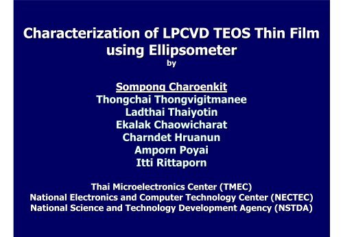
Characterization of LPCVD <strong>TEOS</strong> Thin Filmusing EllipsometerbySompong CharoenkitThongchai ThongvigitmaneeLadthai ThaiyotinEkalak ChaowicharatCharndet HruanunAmporn PoyaiItti RittapornThai Microelectronics Center (TMEC)National Electronics and Computer Technology Center (NECTEC)National Science and Technology Development Agency (NSTDA)
KEY OF THIN FILM GROWTH FOR MICROELECTRONICSBasic Fabrication processconsist of three majorsteps:1. Deposition of <strong>thin</strong><strong>film</strong>s2. Photolithography3. Selective etching ofthe <strong>film</strong>s.
THIN FILM DEPOSITION FOR BASIC ETCH PROCESSTHIN FILM DEPOSITION FOR FABRICATION PROCESS
Outline• Thin <strong>film</strong> technology• LPCVD system• <strong>TEOS</strong> <strong>thin</strong> <strong>film</strong> <strong>deposition</strong>• Characteristics of <strong>TEOS</strong> <strong>thin</strong> <strong>film</strong>s• Conclusion
Outline• Thin <strong>film</strong> technology• LPCVD system• <strong>TEOS</strong> <strong>thin</strong> <strong>film</strong> <strong>deposition</strong>• Characteristics of <strong>TEOS</strong> <strong>thin</strong> <strong>film</strong>s• Conclusion
Thin <strong>film</strong> technologyDeposition technologies can be divided intotwo groups:1. Physical Vapor Deposition (PVD) process2. Chemical Vapor Deposition (CVD) process
Type of Deposition MethodsPhysical Vapor Deposition: PVD- Evaporation- E Beam evaporation- SputteringChemical Vapor Deposition: CVD- Plasma Enhanced CVD (PECVD)- Atmospheric Pressure CVD (APCVD)- Low Pressure CVD (LPCVD)
Outline• Thin <strong>film</strong> technology• LPCVD system• <strong>TEOS</strong> <strong>thin</strong> <strong>film</strong> <strong>deposition</strong>• Characteristics of <strong>TEOS</strong> <strong>thin</strong> <strong>film</strong>s• Conclusion
Low Pressure CVD (LPCVD)Advantage- Moderate <strong>deposition</strong> rates- Very high throughput- Minimal contaminationDisadvantage- Film contamination (reactionproducts and carrier gases)
LPCVD horizontal hot-wall furnace system
SVG LPCVD furnace THERMCO TMX2603at Thai Microelectronics Center (TMEC)frontback
Structure of LPCVD <strong>TEOS</strong> furnaceComputer Control <strong>TEOS</strong> liquid sourceQuartz Boat Gas cabinet & Vacuum System
Outline• Thin <strong>film</strong> technology• LPCVD system• <strong>TEOS</strong> <strong>thin</strong> <strong>film</strong> <strong>deposition</strong>• Characteristics of <strong>TEOS</strong> <strong>thin</strong> <strong>film</strong>s• Conclusion
Step in <strong>film</strong> growth- Gases are introduced into a reactionchamber- Gas species move to the substrate- Reactants are adsorbed on thesubstrate- Film-forming chemical reactions- Desorption and removal of gaseousby-products
Oxide (SiO2) Films Deposition- Silane & Oxygen (300-500C)SiH4 + O2- Tetraethylorthosilicate: <strong>TEOS</strong> (500-800C)Si(OCOC2H5)4700 C450 C SiO2+2H2 SiO2+ by-products- Dichlorosilane & Nitrous (~900C)900 CSiClCl2H2 + 2N2O SiO2+ 2N2 + 2HCl
<strong>TEOS</strong> Films by LPCVDAdvantage- Isolation layer- Step coverage- Hard mask- Moderate <strong>deposition</strong> rateDisadvantage- Bad thickness uniformity (~3% 3%)
~0.5cm ~1cmUniformity (%) = [Standard deviation/ Thickness average] × 100
Process A: A Different Operate PressureTechniqueTemperatureGas flow <strong>TEOS</strong>Operate PressureDeposit TimeWafer spacingLPCVD705 C80 SCCM150, 200, 250, 300 mtorr20 minuteNormalProcess B: B Different TemperatureTechniqueTemperatureGas flow <strong>TEOS</strong>Operate PressureDeposit TimeWafer spacingLPCVD680, 690, 700, 705, 710 C80 SCCM200 mtorr20 minuteNormal
Process C: C Wafer spacingTechniqueTemperatureGas flow <strong>TEOS</strong>Operate PressureDeposit TimeWafer spacingLPCVD705 C80 SCCM175, 200, 225 mtorr20 minuteAdjustmentProcess D: D Different Deposition TimeTechniqueTemperatureGas flow <strong>TEOS</strong>Operate PressureDeposit TimeWafer spacingLPCVD705 C80 SCCM200 mtorr30, 60, 90 minuteAdjustment
Outline• Thin <strong>film</strong> technology• LPCVD system• <strong>TEOS</strong> <strong>thin</strong> <strong>film</strong> <strong>deposition</strong>• Characteristics of <strong>TEOS</strong> <strong>thin</strong> <strong>film</strong>s• Conclusion
Map <strong>TEOS</strong> <strong>film</strong>ELLIPSOMETERThin Film Measurement at Thai Microelectronics Center (TMEC)
Properties of Silicon Dioxide FilmsPropertyThermallyat 1000 CSiH4+4+O2at 450 C<strong>TEOS</strong>at 700 CSiCl2H2+2+N2Oat 900 CCompositionSiO 2SiO 2 (H)SIO 2SiO 2 (Cl)Density(g/cm3 )2.22.12.22.2Refractive index1.461.441.461.46Strength(106 V/cm)>1081010Etch rate (nm/min)(100:1 H2O:HF)3633Etch rate (nm/min)(buffered HF)441204545Step coverage-nonconformalconformalconformalFundamentals of Semiconductor Fabrication (page158)
Properties of <strong>TEOS</strong> Films by LPCVDProperty<strong>TEOS</strong> at 705 CCompositionRefractive index (n)Absorption coefficient (k)Wafer uniformity (%)6 inch waferDeposition rate (nm/min)Etch rate (nm/min)HF3%Step coverageSiO 2~1.450.0000~1.09.266Conformal
<strong>TEOS</strong> Thin Film by LPCVD for Application
Outline• Thin <strong>film</strong> technology• LPCVD system• <strong>TEOS</strong> <strong>thin</strong> <strong>film</strong> <strong>deposition</strong>• Characteristics of <strong>TEOS</strong> <strong>thin</strong> <strong>film</strong>s• Conclusion
ConclusionThe silicon dioxide (<strong>TEOS</strong>) <strong>film</strong>s havewafer uniformity about 1.0 %refractive index about 1.45absorption coefficient of 0.0<strong>deposition</strong> rate of 9.2 nm/minEtch rate (HF3%) of 66 nm/min
AcknowledgementsI would like to give my special thanks to TMEC TeamThai Microelectronics Center (TMEC)National Electronics and Computer Technology Center (NECTEC)National Science and Technology Development Agency (NSTDA)
Thank you for your attention