An Improved VLSI Test Economics Analysis System - Laboratory for ...
An Improved VLSI Test Economics Analysis System - Laboratory for ...
An Improved VLSI Test Economics Analysis System - Laboratory for ...
You also want an ePaper? Increase the reach of your titles
YUMPU automatically turns print PDFs into web optimized ePapers that Google loves.
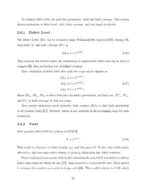
To estimate defect level, we need two parameters: yield and fault coverage. This sectiondiscuss estimation of defect level, yield, fault coverage, and test length in details.2.6.1 Defect LevelThe Defect Level (DL) can be estimated using William-Brown equation [16], relating DLwith yield (Y) and fault coverage (FC) asDL =1, Y 1,FC : (2.46)This equation was derived under the assumption of equiprobable faults and can be used toestimate DL after production test of dened coverage.Thus, estimation of defect level after each test stage can be express as:DL w =1, Y 1,FCw ;DL p =1, Y 1,FCp ;(2.47)DL f =1, Y 1,FC f;where DL w , DL p , DL f is defect level after the wafer, pre-burn-in, and nal test. FC w , FC p ,and FC f is fault coverage of each test stage.More precise estimation needs inductive fault analysis (ILA) to nd fault probabilityof all possible faults [17]. However, layout is not available in oor-planning stage <strong>for</strong> suchestimation.2.6.2 YieldMost popular yield model are poisson model [18]:Y = e , dA : (2.48)This model is a function of defect density ( d ) and chip area (A). In fact, chip yield mainlyaected by chip area since defect density is given by fabrication line defect statistics.Domer indicated more precise yield model estimating the area which is sensitive to defectsrather than using the whole die area [19]. Kim proposed a total sensitive area (TSA) modelto estimate this sensitive area early in design cycle [20]. This model is shown in (2.49) which28


