EE539: Analog Integrated Circuit Design; HW7
EE539: Analog Integrated Circuit Design; HW7
EE539: Analog Integrated Circuit Design; HW7

You also want an ePaper? Increase the reach of your titles
YUMPU automatically turns print PDFs into web optimized ePapers that Google loves.
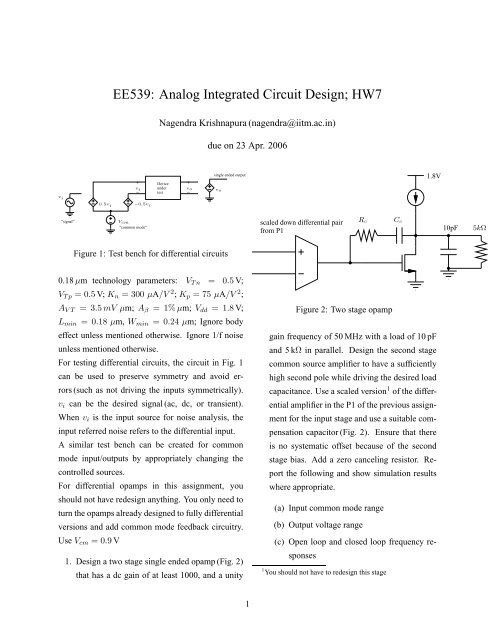
<strong>EE539</strong>: <strong>Analog</strong> <strong>Integrated</strong> <strong>Circuit</strong> <strong>Design</strong>; <strong>HW7</strong>Nagendra Krishnapura (nagendra@iitm.ac.in)due on 23 Apr. 2006++ Devicev iv i−undertestvo−”signal”0.5v i −0.5v iVcm”common mode”single ended outputvoscaled down differential pairfrom P1R c C c1.8V10pF5kΩFigure 1: Test bench for differential circuits0.18 µm technology parameters: V T n = 0.5 V;V T p = 0.5 V; K n = 300 µA/V 2 ; K p = 75 µA/V 2 ;A V T = 3.5 mV µm; A β = 1% µm; V dd = 1.8 V;L min = 0.18 µm, W min = 0.24 µm; Ignore bodyeffect unless mentioned otherwise. Ignore 1/f noiseunless mentioned otherwise.For testing differential circuits, the circuit in Fig. 1can be used to preserve symmetry and avoid errors(such as not driving the inputs symmetrically).v i can be the desired signal (ac, dc, or transient).When v i is the input source for noise analysis, theinput referred noise refers to the differential input.A similar test bench can be created for commonmode input/outputs by appropriately changing thecontrolled sources.For differential opamps in this assignment, youshould not have redesign anything. You only need toturn the opamps already designed to fully differentialversions and add common mode feedback circuitry.Use V cm = 0.9 V1. <strong>Design</strong> a two stage single ended opamp (Fig. 2)that has a dc gain of at least 1000, and a unityFigure 2: Two stage opampgain frequency of 50 MHz with a load of 10 pFand 5 kΩ in parallel. <strong>Design</strong> the second stagecommon source amplifier to have a sufficientlyhigh second pole while driving the desired loadcapacitance. Use a scaled version 1 of the differentialamplifier in the P1 of the previous assignmentfor the input stage and use a suitable compensationcapacitor (Fig. 2). Ensure that thereis no systematic offset because of the secondstage bias. Add a zero canceling resistor. Reportthe following and show simulation resultswhere appropriate.(a) Input common mode range(b) Output voltage range(c) Open loop and closed loop frequency responses1 You should not have to redesign this stage1
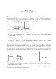
210 pFV dd5 kΩC cmV cm + v iV cmV op5 kΩV onRcmR cmV cm,refdifferential amp load conditionsomit the resistors for folded cascode version10 pFFigure 3: Differential opampto first stage loadC cmV opV onI cmfbtransistors in triode region(pMOS version of this can also be used)Figure 4: Common mode feedback structure forfolded cascode opamp(d) An estimate of poles and zeros of the circuit(open and closed loop)(e) DC sweep of the buffer with input varyingfrom 0 to Vdd(f) Transient response of the unity gain bufferwith a +0.1 V step and a -0.1 V step (use1 ns rise/fall times). Report the slew rateand compare it with the theoretical value.(g) Input referred noise spectral densityidentify1/f noise corner if applicable.(h) Power consumption(i) Show a schematic with all sizes and operatingpoints (g m , g ds , V GS -V T , I D ) of alltransistors and the node voltages.2. Turn the folded cascode opamp designed in assignment6 to a fully differential version. Usethe circuit in Fig. 4 for common mode feedback.Size the CMFB transistors to have 50 mV acrossthem in quiescent condition. Report the follow-Figure 5: Common mode feedback structure for twostage opamping and show simulation results where appropriate.(a) Input common mode range(b) Output voltage range(c) Open loop frequency response(d) An estimate of poles and zeros of the circuit(e) Input(differential) referred noise spectraldensity-identify 1/f noise corner if applicable.(f) Power consumption(g) Show a schematic with all sizes and operatingpoints (g m , g ds , V GS -V T , I D ) of alltransistors and the node voltages.3. Turn the two stage opamp in P1 above into afully differential version. Use the circuit inFig. 5 for common mode feedback. Report thesame quantities as above.4. Use the opamps in P2 and P3 (fully differentialopamps designed earlier) in the samplehold circuit in Fig. 6. Use ideal switches with1 kΩ on resistance. Use f s = 4 MHz and
3φ 2φ 1φ 28 pF8 pF+ V cmV cm ± v i /2 φ 1 v out8 pF−φ 28 pFφ 1φ 2v i = V ip cos(2πf in t)φ 1φ 20 1/f tsFigure 6: Sample and hold circuit10 kΩf in= {1/4, 9/4} MHz (sinusoidal input with1.6 Vppd 2 amplitude) and plot the output waveforms.5. Simulate the response of the circuit in Fig. 7 to adifferential step of 1 V and plot the output. Alsoplot the output for a 0.5 V common mode step.Use the two stage fully differential opamp designedabove.10 kΩv ipv in10 kΩV cm = 0.9 VV cmv ip10 kΩ8 pF10 kΩV cm10 kΩ8 pFv inV cmv ip, v indifferential stepcommon mode stepFigure 7: Inverting amplifier2 Vppd: volts, peak-peak differential