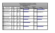
Dr. Jaspal Parganram Bange - North Maharashtra University
Dr. Jaspal Parganram Bange - North Maharashtra University
Dr. Jaspal Parganram Bange - North Maharashtra University

Create successful ePaper yourself
Turn your PDF publications into a flip-book with our unique Google optimized e-Paper software.
<strong>Dr</strong>. <strong>Jaspal</strong> <strong>Parganram</strong> <strong>Bange</strong>01. Full Name : <strong>Dr</strong>. <strong>Jaspal</strong> <strong>Parganram</strong> <strong>Bange</strong>02. Contact Information : Department of Electronics,<strong>North</strong> <strong>Maharashtra</strong> <strong>University</strong>,Post Box # 80,JALGAON – 425001 (M.S.)E-mail : jpbange@nmu.ac.injaspal_bange@hotmail.comTelephone No. : 0257-2257475 Ext. 10803. Education Qualification :Mobile : 09422782762Examination<strong>University</strong>/BoardMonth & Yearof PassingSubjectsSPL/Gen% ofMarksClass/Div/GradeawardedPh.D.Master’sDegreeBachelor’sDegreeNMU*,JalgaonNMU*,JalgaonNMU*,JalgaonApril 2008 Electronics ---- AwardedDecember 1999 Electronics 66.30 IstJune 1997 Electronics 64.16 IstHigherSecondaryPune March 1993 Science 58.67 IIndMatriculationSSCPune March 1991 General 61.71 Ist* NMU: <strong>North</strong> <strong>Maharashtra</strong> <strong>University</strong>04. Teaching Experience :Sr. No. Post Organization Period01 Assistant ProfessorDepartment of Electronics,<strong>North</strong> <strong>Maharashtra</strong><strong>University</strong>, Jalgaon, India09 th Aug. 2012toDate1
05. Area of Research/Expertise : Optoelectronic, Dielectric, Semiconductormaterials, Polymer waveguides.06. Awards/Fellowships/prizes received :Sr.No.01 Post-doc FellowPost Organization PeriodAdvanced Technology ResearchCenter (GU-ATEC),Gunma <strong>University</strong>,Kiryu, JAPAN16 th Feb. 2009to31 st March 201102Research AssociateIn Council for Scientificand Industrial Research(CSIR) Sponsored projectDepartment of Electronics,<strong>North</strong> <strong>Maharashtra</strong> <strong>University</strong>,Jalgaon20 th Feb. 2008to30 th June 20080304Research ScientistIn Instrument Researchand DevelopmentEstablishment (IRDE) –Defence Research andDevelopmentOrganization (DRDO)Sponsored projectProject AssociateIn Department of Scienceand Technology (DST)Sponsored project Phase-II-EDepartment of Electronics,<strong>North</strong> <strong>Maharashtra</strong> <strong>University</strong>,JalgaonDepartment of Electronics,<strong>North</strong> <strong>Maharashtra</strong> <strong>University</strong>,Jalgaon1 st March 2005to28 th Feb. 20062 nd May 2002to1 st May 200405Project AssociateIn Department of Scienceand Technology (DST)Sponsored project Phase-IIDepartment of Electronics,<strong>North</strong> <strong>Maharashtra</strong> <strong>University</strong>,Jalgaon1 st Sept. 2001to28 th Feb. 200206Project AssistantIn Council for Scientificand Industrial Research(CSIR) Sponsored projectDepartment of Electronics,<strong>North</strong> <strong>Maharashtra</strong> <strong>University</strong>,Jalgaon5 th July 2001to30 th Aug. 200107Junior Research FellowIn All India Council forTechnical Education(AICTE) Sponsored projectDepartment of Electronics,<strong>North</strong> <strong>Maharashtra</strong> <strong>University</strong>,Jalgaon1 st Feb. 2000to31 st Jan. 200107. Number of Post Doc Students : Nil2
08. Number of Ph.D. Students Completed : Nil09. Number of Ph.D. students on going : Nil10. Number of M. Phil. Students completed : Nil11. Number of M. Phil. Students on going : Nil12. Number of Books Written : Nil13. Number of Patents : Nil14. Research Publications :Articles in Journals:1. <strong>Jaspal</strong> <strong>Parganram</strong> <strong>Bange</strong>, Mayank Kumar Singh, Kazusa Kano, Kenta Miura andOsamu Hanaizumi, “Structural analysis of RF sputtered Er doped Ta2O5 films”,Journal of Key Engineering Materials, Vol. 459, 2011, 32-37 (Impact Factor 0.340).2. J. P. <strong>Bange</strong>, Lalit S. Patil and D. K. Gautam, “Effect of OMCTS flow rate on SiO2 filmsgrown by flame Hydrolysis deposition”, Journal of Optoelectronics and AdvancedMaterials Rapid Communication, Vol. 4(4), 2010, 584-587 (Impact Factor 0.304).3. <strong>Jaspal</strong> P. <strong>Bange</strong>, Lalit S. Patil and D. K. Gautam, “Influence of Titanium-tetraisopropoxideflow in TiO2 doped SiO2 films for waveguide applications”, Journal ofOptoelectronics & Biomedical Materials, Vol. 6, No.4, 2009, 319-324 (Impact Factor0.0).4. Mayank Kumar Singh, Genjoh Fusegi, Kazusa Kano, <strong>Jaspal</strong> <strong>Parganram</strong> <strong>Bange</strong>, KentaMiura and Osamu Hanaizumi, “Intense Photoluminescence from erbium-dopedtantalum oxide thin films deposited by sputtering”, IEICE Electronics Express, Vol. 6,No. 23, 2009, 1676-1382 (Impact Factor 0.46).5. Deepak R. Patil, Lalit S. Patil, <strong>Jaspal</strong> P. <strong>Bange</strong>, D. K. Gautam, “Deposition of orientednanocrystaline TiO2 films”, Optoelectronics And Advanced Materials, Vol. 10, No.12, 2008, 3251-3256 (Impact Factor 0.457).6. J. P. <strong>Bange</strong>, L. S. Patil and D. K. Gautam, “Growth and characterization of SiO2 filmsdeposited by flame hydrolysis deposition system for photonics device application”,Progress In Electromagnetics Research M, Vol. 3, 2008, 165-175 (Impact Factor 0.0).7. R. S. Dubey, L. S. Patil, J. P. <strong>Bange</strong>, D. K. Gautam, “Fabrication of one-dimensionalphotonic crystals using porous silicon layers”, Optoelectronics And AdvancedMaterials – Rapid Communications, Vol. 1, No. 12, 2007, 655-658 (Impact Factor0.304).3
8. A.M. Mahajan, L.S. Patil, J. P. <strong>Bange</strong> and D.K. Gautam, “TEOS-PECVD System for highgrowth rate deposition of SiO2 films”, ‘Vacuum’, Vol. 79, 2005, 194-202 (ImpactFactor 1.317).9. L. S. Patil, R. K. Pandey, <strong>Jaspal</strong> P. <strong>Bange</strong>, S. A. Gaikwad and D. K. Gautam, “Effect ofdeposition temperature on the chemical properties of thermally deposited SiliconNitride Films”, Optical Material, Vol. 27, 2005, 663-670 (Impact Factor 2.023).10. R. K. Pandey, L. S. Patil, J. P. <strong>Bange</strong>, D. K. Gautam, “Growth and Characterization ofSilicon Nitride films for optoelectronics application”, Optical Material, Vol. 27, 2004,139-146, (Impact Factor 2.023).11. A. M. Mahajan, L. S. Patil, J. P. <strong>Bange</strong>, D. K. Gautam, “Growth of SiO2 films byTEOS_PECVD system for microelectronics applications”, Journal of Surface Coatings& Technology, Vol. 183,No. 2, 2004, 295-300 (Impact Factor 1.867).12. R. K. Pandey, L. S. Patil, J. P. <strong>Bange</strong>, D. R. Patil, A. M. Mahajan D. S. Patil, D. K.Gautam, “Growth and Characterization of SiON thin films by using thermal-CVDmachine”, Optical Materials, Vol. 25, 2004, 1-7 (Impact Factor 2.023).13. A. M. Mahajan, L.S. Patil, J. P. <strong>Bange</strong>, and D. K. Gautam, “Growth andCharacterization of SiO2 films for the fabrication of Optical Waveguides”, Journal ofOptics, Vol.31, No.2, 2002, 53-58 (Impact Factor 0.0).Articles in Books:1. <strong>Jaspal</strong> P. <strong>Bange</strong>, Lalit S. Patil and D. K. Gautam, “Growth of SiO2 films by FlameHydrolysis Deposition System for Biosensor Application”, Frontiers of Microwave andOptoelectronics, ISBN 978-81-89927-19-6, 2008, 168-176.2. R. K. Pandey, L. S. Patil, J. P. <strong>Bange</strong>, R. S. Dubey, S. A. Gaikwad and D. K. Gautam,“Effect of deposition temperature on the properties of Silicon nitride films grown bythermal CVD system”, Frontiers of Microwave and Optoelectronics, ISBN 81-88342-44-0, 2004, 298-302.Articles in National / International Conference Proceedings:1. <strong>Jaspal</strong> <strong>Parganram</strong> <strong>Bange</strong>,Yuki Machida, Masato Uehara, Amarachukwu ValentineUmenyi,Kenta Miura and Osamu Hanaizumi, “Design and analysis of single modepolymer waveguide using PBW technique”, Proceedings of International Conferenceon Advanced Micro-Device Engineering, AMDE-2010, Japan, 2P37.2. <strong>Jaspal</strong> P. <strong>Bange</strong>, L.S. Patil and D. K. Gautam, “Comparison of TiO2-Doped SiO2 Filmsfrom Two Organosilicon Precursors”, Asia Communications and PhotonicsConference and Exhibition, ACP2010, Shanghai, China, P62.4
3. <strong>Jaspal</strong> P. <strong>Bange</strong>, L.S. Patil and D. K. Gautam, “Effect of substrate temperature onproperties of SiO2 films by Flame Hydrolysis”, Proceedings of Internationalconference on MEMS and Optoelectronics Technologies, ICMOT-2010, India, 50-52.4. <strong>Jaspal</strong> P. <strong>Bange</strong>, L.S. Patil and D. K. Gautam, “Synthesis of TiO2 Films by FlameHydrolysis Deposition System”, Proceedings of International Conference onNanotechnology and Biosensors, ICNB-2010, India, 82.5. Mayank Kumar Singh, Genjoh Fusegi, Kazusa Kano, <strong>Jaspal</strong> P. <strong>Bange</strong>, Kenta Miura andOsamu Hanaizumi, “Fabrication and optimization of green light emitting Er-Ta2O5films”, International conference on Advanced Micro-Device Engineering, AMDE-2009, Japan, 2P25, PP 103.6. <strong>Jaspal</strong> P. <strong>Bange</strong>, O. Hanaizumi, Lalit S. Patil and D. K. Gautam, “TiO2-doped SiO2 filmsdeposited by Flame Hydrolysis Deposition system for waveguide applications”,International Conference on Optics and Photonics-ICOP 2009, Chandigarh, India,B3.6.7. <strong>Jaspal</strong> P. <strong>Bange</strong>, L. S. Patil and D. K. Gautam, “SiO2-TiO2 Nano Composite Film byFlame Hydrolysis Deposition”, Asia Communications and Photonics Conference andExhibition, ACP2009, Shanghai, China ISBN: 978-1-55752-877-3, THG3.8. <strong>Jaspal</strong> P. <strong>Bange</strong>, L. S. Patil and D. K. Gautam, “Effect of titanium tetra-isopropoxideflow rate on SiO2-TiO2 composite films by FHD”, International Conf. on AdvancedMaterials, ICAM2009, Rio de Janeiro, Brazil, A576.9. <strong>Jaspal</strong> P. <strong>Bange</strong>, Lalit S. Patil and D. K. Gautam, “Effect of annealing on the filmsgrown by Flame Hydrolysis Deposition system”, Proceeding of InternationalConference on Electronics and Photonics Materials, Devices and System EPMDS –2006, India, B39-B41.10. <strong>Jaspal</strong> P. <strong>Bange</strong>, L. S. Patil and D. K. Gautam, “Automation of Flame HydrolysisDeposition system for optical device fabrication”, Proceeding of National Symposiumon Instrumentation NSI – 30, India, 885-894.11. V. P. Chavan, E. R. Khan, Rajdeep Gautam, M. P. Bhole, <strong>Jaspal</strong> P. <strong>Bange</strong>, D. S. Patiland D. K. Gautam, “Monitoring and control of gas flow for the effective deposition offilms in MOCVD for quantum well devices”, Proceeding of International Conferenceon Optoelectronics Technology, ICOT – 2004, India, 472-480.12. <strong>Jaspal</strong> P. <strong>Bange</strong>, Lalit S. Patil, Vinod Patil, D. Bhavar, Suchita Bhangale and D. K.Gautam, “Automation of process parameters of indigenously developed FHDsystem”, Proceeding of International Conference on Optoelectronics Technology,ICOT – 2004, India, 453-461.13. A. M. Mahajan, L. S. Patil, J. P. <strong>Bange</strong> and D. K. Gautam, “Effect of variation in O2 /TEOS flow ration on properties of SiO2 films deposited by PECVD”, Proc. of Int. Conf.on Optoelectronics, Fiber optics and Photonics, PHOTONICS – 2002, Mumbai, India,OMDP-17, PP 286.5
14. A. M. Mahajan, L. S. Patil, J. P. <strong>Bange</strong> and D. K. Gautam, “Effect of Chamber PressureVariation on Refractive Index of SiO2 Films Developed by PECVD”, Proc. of int.conference on Broad Band Optical Fiber Communication Technology, BBOFCT –2001, India, 283-286.15. Chitrarekha Chaudhari, Dnyaneshwar S. Patil, L. S. Patil, J. P. <strong>Bange</strong> and D. K.Gautam, “Technology development for the optical rib waveguide structures onsilicon substrate”, Proc. of international conference on fiber optics and photonics,PHOTONICS 2000, India, 786-788.15. Research project completed : Nil16. Research project on going : Nil17. Consultancy Projects : Nil18. Research project submitted : Nil19. Scientific collaborators : Nil20. Memberships : Nil21. Administrative Work experience :Sr. No. Post Organization Period01 Senior Project OfficerLovely Professional <strong>University</strong>,Jalandhar - Delhi G.T. Road (NH-1),Phagwara, Punjab (India) - 14441116 th Jan. 2012to02 nd Aug. 201222. Working experience with national bodies/national exposures : Nil23. Working experience with international bodies/international exposures : Nil24. Leadership experience : Nil25. Serving on Editorial Boards : Nil26. Technology Transferred : Nil27. Any other activity done/going on :Organised the following activities at the Department of Electronics, <strong>North</strong><strong>Maharashtra</strong> <strong>University</strong>, Jalgaon1) Worksop on “Programmable Logic Controllers” during 25-26 th January 2013.2) Science day celebration on 28 th February 2013.6
28. Contribution to <strong>University</strong>/School/Department :During the period 1 st Feb. 2000 to 30 th June 2008 I have been actively engaged in thedevelopment of Research Laboratory at the department of Electronics along withsuccessful completion of the government funded research projects. The facilitiesdeveloped indigenously includes the following1) Class 10000 clean room for semiconductor material processing.2) Design and fabrication of Spin coating machine.3) Design and fabrication of Thermal Chemical Vapour Deposition (CVD) systemfor SiO2 films.4) Design and fabrication of Thermal Chemical Vapour Deposition (CVD) systemfor Silicon Nitride and Silicon oxynitride films.5) Design and fabrication of vertical Thermal Chemical Vapour Deposition (CVD)system.6) Design and fabrication of Liquid Phase Epitaxy system (LPE).7) Design and fabrication of Plasma Enhanced Chemical Vapour Depositionsystem (PECVD).8) Design and fabrication of Flame Hydrolysis Deposition (FHD) system.7