NE555, NE555Y, SA555, SE555, SE555C PRECISION TIMERS
NE555, NE555Y, SA555, SE555, SE555C PRECISION TIMERS
NE555, NE555Y, SA555, SE555, SE555C PRECISION TIMERS

You also want an ePaper? Increase the reach of your titles
YUMPU automatically turns print PDFs into web optimized ePapers that Google loves.
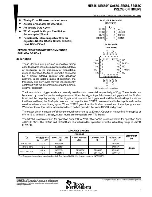
<strong>NE555</strong>, <strong>NE555</strong>Y, <strong>SA555</strong>, <strong>SE555</strong>, <strong>SE555</strong>C<strong>PRECISION</strong> <strong>TIMERS</strong>SLFS022 – SEPTEMBER 1973 – REVISED FEBRUARY 1992Timing From Microseconds to HoursAstable or Monostable OperationAdjustable Duty CycleTTL-Compatible Output Can Sink orSource up to 200 mAFunctionally Interchangeable With theSignetics <strong>NE555</strong>, <strong>SA555</strong>, <strong>SE555</strong>, <strong>SE555</strong>C;Have Same Pinout<strong>SE555</strong>C FROM TI IS NOT RECOMMENDEDFOR NEW DESIGNSGNDTRIGOUTRESETD, JG, OR P PACKAGE(TOP VIEW)12348765FK PACKAGE(TOP VIEW)NCGNDNCVCCNCV CCDISCHTHRESCONTdescriptionThese devices are precision monolithic timingcircuits capable of producing accurate time delaysor oscillation. In the time-delay or monostablemode of operation, the timed interval is controlledby a single external resistor and capacitornetwork. In the astable mode of operation, thefrequency and duty cycle may be independentlycontrolled with two external resistors and a singleexternal capacitor.NCTRIGNCOUTNC342 1 20 19185671716158149 10 11 12 13NCRESETNCCONTNCNC–No internal connectionNCDISCHNCTHRESNCThe threshold and trigger levels are normally two-thirds and one-third, respectively, of V CC . These levels canbe altered by use of the control voltage terminal. When the trigger input falls below the trigger level, the flip-flopis set and the output goes high. If the trigger input is above the trigger level and the threshold input is abovethe threshold level, the flip-flop is reset and the output is low. RESET can override all other inputs and can beused to initiate a new timing cycle. When RESET goes low, the flip-flop is reset and the output goes low.Whenever the output is low, a low-impedance path is provided between DISCH and ground.The output circuit is capable of sinking or sourcing current up to 200 mA. Operation is specified for supplies of5 V to 15 V. With a 5-V supply, output levels are compatible with TTL inputs.The <strong>NE555</strong> is characterized for operation from 0°C to 70°C. The <strong>SA555</strong> is characterized for operation from–40°C to 85°C. The <strong>SE555</strong> and <strong>SE555</strong>C are characterized for operation over the full military range of –55°Cto 125°C.AVAILABLE OPTIONSPACKAGETA VTHRES max SMALL OUTLINE CHIP CARRIER CERAMIC DIP PLASTIC DIPVCC = 15 V(D)(FK)(J)(P)0°C to 70°C 11.2 V <strong>NE555</strong>D <strong>NE555</strong>P–40°C to 85°C 11.2 V <strong>SA555</strong>D <strong>SA555</strong>P–55°C to 125°C10.6 V11.2 V<strong>SE555</strong>D<strong>SE555</strong>CD<strong>SE555</strong>FK<strong>SE555</strong>CFK<strong>SE555</strong>JG<strong>SE555</strong>CJGThe D package is available taped and reeled. Add the suffix R to the device type (e.g., <strong>NE555</strong>DR).<strong>SE555</strong>P<strong>SE555</strong>CPCHIP FORM(Y)<strong>NE555</strong>YPRODUCTION DATA information is current as of publication date.Products conform to specifications per the terms of Texas Instrumentsstandard warranty. Production processing does not necessarily includetesting of all parameters.Copyright © 1992, Texas Instruments IncorporatedPOST OFFICE BOX 655303 • DALLAS, TEXAS 752651
<strong>NE555</strong>, <strong>NE555</strong>Y, <strong>SA555</strong>, <strong>SE555</strong>, <strong>SE555</strong>C<strong>PRECISION</strong> <strong>TIMERS</strong>SLFS022 – SEPTEMBER 1973 – REVISED FEBRUARY 1992FUNCTION TABLERESET TRIGGER VOLTAGE† THRESHOLD VOLTAGE† OUTPUT DISCHARGE SWITCHLow Irrelevant Irrelevant Low OnHigh < 1/3 VDD Irrelevant High OffHigh > 1/3 VDD > 2/3 VDD Low OnHigh > 1/3 VDD < 2/3 VDD As previously established† Voltage levels shown are nominal.functional block diagramTHRESVCC8CONT5R6RESET4R1ÎR Î Î13OUTSÎRTRIG2RÎÎÎÎ1GND7DISCHRESET can override TRIG, which can override THRES.Pin numbers shown are for the D, JG, and P packages only.2 POST OFFICE BOX 655303 • DALLAS, TEXAS 75265
<strong>NE555</strong>, <strong>NE555</strong>Y, <strong>SA555</strong>, <strong>SE555</strong>, <strong>SE555</strong>C<strong>PRECISION</strong> <strong>TIMERS</strong>SLFS022 – SEPTEMBER 1973 – REVISED FEBRUARY 1992chip informationThese chips, properly assembled, display characteristics similar to the <strong>NE555</strong> (see electrical table for <strong>NE555</strong>Y).Thermal compression or ultrasonic bonding may be used on the doped aluminum bonding pads. Chips may bemounted with conductive epoxy or a gold-silicon preform.BONDING PAD ASSIGNMENTSVCC(8)CONT(5)RESET(4)(4)(3)(2)(6)THRESRRR1RS1(3)OUTTRIG(2)41(1)R(1)GND(7)DISCH(5)(8)CHIP THICKNESS: 15 TYPICALBONDING PADS: 4 × 4 MINIMUM(6)(7)TJ max = 150° CTOLERANCES ARE ± 10%42ALL DIMENSIONS ARE IN MILSPIN (1) INTERNALLY CONNECTEDTO BACKSIDE OF CHIPPOST OFFICE BOX 655303 • DALLAS, TEXAS 752653
<strong>NE555</strong>, <strong>NE555</strong>Y, <strong>SA555</strong>, <strong>SE555</strong>, <strong>SE555</strong>C<strong>PRECISION</strong> <strong>TIMERS</strong>SLFS022 – SEPTEMBER 1973 – REVISED FEBRUARY 1992absolute maximum ratings over operating free-air temperature range (unless otherwise noted)NOTE 1:Supply voltage, V CC (See Note 1) . . . . . . . . . . . . . . . . . . . . . . . . . . . . . . . . . . . . . . . . . . . . . . . . . . . . . . . . . . . . 18 VInput voltage (CONT, RESET, THRES, and TRIG) . . . . . . . . . . . . . . . . . . . . . . . . . . . . . . . . . . . . . . . . . . . . . . V CCOutput current . . . . . . . . . . . . . . . . . . . . . . . . . . . . . . . . . . . . . . . . . . . . . . . . . . . . . . . . . . . . . . . . . . . . . . . . . ±225 mAContinuous total dissipation . . . . . . . . . . . . . . . . . . . . . . . . . . . . . . . . . . . . . . . . . . . See Dissipation Rating TableOperating free-air temperature range: <strong>NE555</strong> . . . . . . . . . . . . . . . . . . . . . . . . . . . . . . . . . . . . . . . . . 0°C to 70°C<strong>SA555</strong> . . . . . . . . . . . . . . . . . . . . . . . . . . . . . . . . . . . . . . . . –40°C to 85°C<strong>SE555</strong>, <strong>SE555</strong>C . . . . . . . . . . . . . . . . . . . . . . . . . . . . . . –55°C to 125°CStorage temperature range . . . . . . . . . . . . . . . . . . . . . . . . . . . . . . . . . . . . . . . . . . . . . . . . . . . . . . . . –65°C to 150°CCase temperature for 60 seconds: FK package . . . . . . . . . . . . . . . . . . . . . . . . . . . . . . . . . . . . . . . . . . . . . . 260°CLead temperature 1,6 mm (1/16 inch) from case for 10 seconds: D or P package . . . . . . . . . . . . . . . . . 260°CLead temperature 1,6 mm (1/16 inch) from case for 60 seconds: JG package . . . . . . . . . . . . . . . . . . . . 300°CAll voltage values are with respect to network ground terminal.PACKAGETA ≤ 25°CPOWER RATINGDISSIPATION RATING TABLEDERATING FACTORABOVE TA = 25°CTA = 70°CPOWER RATINGTA = 85°CPOWER RATINGTA = 125°CPOWER RATINGD 725 mW 5.8 mW/°C 464 mW 377 mW N/AFK 1375 mW 11.0 mW/°C 880 mW 715 mW 275 mWJG (<strong>SE555</strong>, <strong>SE555</strong>C) 1050 mW 8.4 mW/°C 672 mW 546 mW 210 mWJG (<strong>SA555</strong>, <strong>NE555</strong>C) 825 mW 6.6 mW/°C 528 mW 429 mW N/AP 1000 mW 8.0 mW/°C 640 mW 520 mW N/Arecommended operating conditions<strong>NE555</strong> <strong>SA555</strong> <strong>SE555</strong> <strong>SE555</strong>CMIN MAX MIN MAX MIN MAX MIN MAXUNITSupply voltage, VCC 4.5 16 4.5 16 4.5 18 4.5 16 VInput voltage (CONT, RESET, THRES, and TRIG) VCC VCC VCC VCC VOutput current ±200 ±200 ±200 ±200 mAOperating free-air temperature, TA 0 70 –40 85 –55 125 –55 125 °C4 POST OFFICE BOX 655303 • DALLAS, TEXAS 75265
<strong>NE555</strong>, <strong>NE555</strong>Y, <strong>SA555</strong>, <strong>SE555</strong>, <strong>SE555</strong>C<strong>PRECISION</strong> <strong>TIMERS</strong>SLFS022 – SEPTEMBER 1973 – REVISED FEBRUARY 1992electrical characteristics, V CC = 5 V to 15 V, T A = 25°C (unless otherwise noted)PARAMETERTHRES voltage level<strong>NE555</strong>, <strong>SA555</strong>,<strong>SE555</strong>TEST CONDITIONS<strong>SE555</strong>CMIN TYP MAX MIN TYP MAXVCC = 15 V 9.4 10 10.6 8.8 10 11.2VCC = 5 V 2.7 3.3 4 2.4 3.3 4.2THRES current (see Note 2) 30 250 30 250 nATRIG voltage levelVCC = 15 V 4.8 5 5.2 4.5 5 5.6VCC = 5 V 1.45 1.67 1.9 1.1 1.67 2.2TRIG current TRIG at 0 V 0.5 0.9 0.5 2 µARESET voltage level 0.3 0.7 1 0.3 0.7 1 VRESET currentRESET at VCC 0.1 0.4 0.1 0.4RESET at 0 V –0.4 –1 –0.4 –1.5DISCH switch off-state current 20 100 20 100 nACONT voltage (open circuit)Low-level output voltageHigh-level output voltageSupply currentVCC = 15 V 9.6 10 10.4 9 10 11VCC = 5 V 2.9 3.3 3.8 2.6 3.3 4VCC =15VVCC =5VVCC =15VIOL = 10 mA 0.1 0.15 0.1 0.25IOL = 50 mA 0.4 0.5 0.4 0.75IOL = 100 mA 2 2.2 2 2.5IOL = 200 mA 2.5 2.5IOL = 5 mA 0.1 0.2 0.1 0.35IOL = 8 mA 0.15 0.25 0.15 0.4IOH = – 100 mA 13 13.3 12.75 13.3IOH = – 200 mA 12.5 12.5 VVCC = 5 V IOH = – 100 mA 3 3.3 2.75 3.3V CC = 15 V 10 12 10 15Output low, No loadV CC = 5 V 3 5 3 6V CC = 15 V 9 10 9 13Output high, No loadV CC = 5 V 2 4 2 5UNITVVmAVVmANOTE 2:This parameter influences the maximum value of the timing resistors RA and RB in the circuit of Figure 12. For example, whenVCC = 5 V, the maximum value is R = RA + RB ≈ 3.4 MΩ, and for VCC = 15 V, the maximum value is 10 MΩ.operating characteristics, V CC = 5 V and 15 VPARAMETERInitial error of timing interval‡Each timer, monostable§Each timer, astableTESTCONDITIONS†TA A =25°CTemperature coefficient Each timer, monostable§ A of timing intervalTA = MIN to MAXEach timer, astableSupply voltage sensitivity Each timer, monostable§ A =25°Cof timing intervalTA Each timer, astable<strong>SE555</strong><strong>NE555</strong>, <strong>SA555</strong>,<strong>SE555</strong>CMIN TYP MAX MIN TYP MAX0.5% 1.5% 1% 3%1.5% 2.25%30 100 5090 1500.05 0.2 0.1 0.50.15 0.3Output pulse rise time CL L = 15 pF, 100 200 100 300Output pulse fall timeTA = 25°C 100 200 100 300UNITppm/°C† For conditions shown as MIN or MAX, use the appropriate value specified under recommended operating conditions.‡ Timing interval error is defined as the difference between the measured value and the average value of a random sample from each processrun.§ Values specified are for a device in a monostable circuit similar to Figure 9, with component values as follow: RA = 2 kΩ to 100 kΩ, C = 0.1 µF. Values specified are for a device in an astable circuit similar to Figure 12, with component values as follow: RA = 1 kΩ to 100 kΩ, C = 0.1 µF.%/VnsPOST OFFICE BOX 655303 • DALLAS, TEXAS 752655
<strong>NE555</strong>, <strong>NE555</strong>Y, <strong>SA555</strong>, <strong>SE555</strong>, <strong>SE555</strong>C<strong>PRECISION</strong> <strong>TIMERS</strong>SLFS022 – SEPTEMBER 1973 – REVISED FEBRUARY 1992electrical characteristics, V CC = 5 V to 15 V, T A = 25°C (unless otherwise noted)THRES voltage levelPARAMETER TEST CONDITIONS MIN TYP MAX UNITVCC = 15 V 8.8 10 11.2VCC = 5 V 2.4 3.3 4.2THRES current (see Note 2) 30 250 nATRIG voltage levelVCC = 15 V 4.5 5 5.6VCC = 5 V 1.1 1.67 2.2TRIG current TRIG at 0 V 0.5 2 µARESET voltage level 0.3 0.7 1 VRESET currentRESET at VCC 0.1 0.4RESET at 0 V –0.4 –1.5DISCH switch off-state current 20 100 nACONT voltage (open circuit)Low-level output voltageHigh-level output voltageSupply currentNOTE 2:VCC = 15 V 9 10 11VCC = 5 V 2.6 3.3 4VCC =15VVCC =5VVCC =15VIOL = 10 mA 0.1 0.25IOL = 50 mA 0.4 0.75IOL = 100 mA 2 2.5IOL = 200 mA 2.5IOL = 5 mA 0.1 0.35IOL = 8 mA 0.15 0.4IOH = – 100 mA 12.75 13.3VVmAIOH = – 200 mA 12.5 VVCC = 5 V IOH = – 100 mA 2.75 3.3Output low, No loadOutput high, No loadVCC = 15 V 10 15VCC = 5 V 3 6VCC = 15 V 9 13VCC = 5 V 2 5This parameter influences the maximum value of the timing resistors RA and RB in the circuit of Figure 12. For example, whenVCC = 5 V, the maximum value is R = RA + RB ≈ 3.4 MΩ, and for VCC = 15 V, the maximum value is 10 MΩoperating characteristics, V CC = 5 V and 15 V, T A = 25°C (unless otherwise noted)Initial error of timing interval†Supply voltage sensitivity of timing intervalPARAMETERVVmATESTMIN TYP MAX UNITCONDITIONSEach timer, monostable‡ 1% 3%Each timer, astable§ 2.25%Each timer, monostable‡ 0.1 0.5Each timer, astable§ 0.3Output pulse rise time100 300CL =15pFnsOutput pulse fall time100 300† Timing interval error is defined as the difference between the measured value and the average value of a random sample from each processrun.‡ Values specified are for a device in a monostable circuit similar to Figure 9, with component values as follow: RA = 2 kΩ to 100 kΩ, C = 0.1 µF.§ Values specified are for a device in an astable circuit similar to Figure 12, with component values as follow: RA = 1 kΩ to 100 kΩ, C = 0.1 µF.%/V6 POST OFFICE BOX 655303 • DALLAS, TEXAS 75265
<strong>NE555</strong>, <strong>NE555</strong>Y, <strong>SA555</strong>, <strong>SE555</strong>, <strong>SE555</strong>C<strong>PRECISION</strong> <strong>TIMERS</strong>TYPICAL CHARACTERISTICS †SLFS022 – SEPTEMBER 1973 – REVISED FEBRUARY 1992107LOW-LEVEL OUTPUT VOLTAGEvsLOW-LEVEL OUTPUT CURRENTVCC = 5 VÏÏÏÏ107LOW-LEVEL OUTPUT VOLTAGEvsLOW-LEVEL OUTPUT CURRENTVCC = 10 V– Low-Level Output Voltage – V4210.70.40.20.10.07ÏÏÏÏTA = – 55°CTA = 25°CÏÏÏÏÏÏÏÏÏÏÏÏÏÏÏÏÏTA = 125°C– Low-Level Output Voltage – V4210.70.40.20.10.07ÏÏÏÏÏÏÏÏÏÏTA = 25°CTA= – 55°CÏÏÏÏÏÏÏÏTA = 125°CÏÏÏÏÏÏÏÏV OL0.04V OL0.040.020.020.011 2 4 7 10 20 40 70 100IOL – Low-Level Output Current – mAFigure 10.011 2 4 7 10 20 40 70 100IOL – Low-Level Output Current – mAFigure 2– Low-Level Output Voltage – VV OL1074210.70.40.20.10.070.04LOW-LEVEL OUTPUT VOLTAGEvsLOW-LEVEL OUTPUT CURRENTVCC = 15 VÏÏÏÏÏÏÏÏTA = 125°CTA = 25°CTA = – 55°CV CC – V OH – Voltage Drop – VDROP BETWEEN SUPPLY VOLTAGE AND OUTPUTvsHIGH-LEVEL OUTPUT CURRENT2.0TA = – 55°C ÏÏÏÏ1.81.61.41.210.80.60.4TA = 25°CÏÏÏÏÏÏÏÏTA = 125°CÏÏÏÏ0.020.011 2 4 7 10 20 40 70 100IOL – Low-Level Output Current – mAFigure 30.2ÏÏÏÏÏÏVCC = 5 V to 15 V01 2 4 7 10IOH – High-Level Output Current – mAFigure 4204070100†Data for temperatures below 0°C and above 70°C are applicable for <strong>SE555</strong> circuits only.POST OFFICE BOX 655303 • DALLAS, TEXAS 752657
<strong>NE555</strong>, <strong>NE555</strong>Y, <strong>SA555</strong>, <strong>SE555</strong>, <strong>SE555</strong>C<strong>PRECISION</strong> <strong>TIMERS</strong>SLFS022 – SEPTEMBER 1973 – REVISED FEBRUARY 1992TYPICAL CHARACTERISTICS †SUPPLY CURRENTvsSUPPLY VOLTAGENORMALIZED OUTPUT PULSE DURATION(MONOSTABLE OPERATION)vsSUPPLY VOLTAGE– Supply Current – mAICC10987654321Output Low,No LoadTA = 25°CTA = –55°CTA = 125°CPulse Duration Relative to Value at VCC = 10 V1.0151.0101.00510.9950.99005 6 7 8 9 10 11 12 13 14 15VCC – Supply Voltage – VFigure 50.9850 5 10VCC – Supply Voltage – VFigure 615 20Pulse Duration Relative to Value at T A = 25 ° C1.0151.0101.00510.9950.990NORMALIZED OUTPUT PULSE DURATION(MONOSTABLE OPERATION)vsFREE-AIR TEMPERATUREVCC = 10 V– Propagation Delay Time – nst PD30025020015010050PROPAGATION DELAY TIMEvsLOWEST VOLTAGE LEVELOF TRIGGER PULSETA = –55°CTA = 0°CTA = 125°CTA = 70°CTA = 25°C0.985–75 –50 –25 0 25 50 75 100 125TA – Free-Air Temperature – °CFigure 700 0.1 x VCC 0.2 x VCC 0.3 x VCC 0.4 x VCCLowest Voltage Level of Trigger PulseFigure 8†Data for temperatures below 0°C and above 70°C are applicable for <strong>SE555</strong> circuits only.8 POST OFFICE BOX 655303 • DALLAS, TEXAS 75265
ÏÏÏÏÏÏÏÏÏÏ<strong>NE555</strong>, <strong>NE555</strong>Y, <strong>SA555</strong>, <strong>SE555</strong>, <strong>SE555</strong>C<strong>PRECISION</strong> <strong>TIMERS</strong>APPLICATION INFORMATIONSLFS022 – SEPTEMBER 1973 – REVISED FEBRUARY 1992monostable operationFor monostable operation, any of these timers may be connected as shown in Figure 9. If the output is low,application of a negative-going pulse to TRIG sets the flip-flop (Q goes low), drives the output high, and turnsoff Q1. Capacitor C is then charged through R A until the voltage across the capacitor reaches the thresholdvoltage of THRES input. If TRIG has returned to a high level, the output of the threshold comparator will resetthe flip-flop (Q goes high), drive the output low, and discharge C through Q1.VCC(5 V to 15 V)RA = 9.1 kΩCL = 0.01 µFRL = 1 kΩSee Figure 9ÏÏÏÏÏÏÏÏÏÏInputRA476ÎÎ2CONTRESETDISCHTHRESTRIG5 8VCCOUTGND13RLOutputVoltage – 2 V/divInput VoltageOutput VoltageCapacitor VoltagePin numbers shown are for the D, JG, and P packages.Figure 9. Circuit for Monostable OperationMonostable operation is initiated when TRIGvoltage falls below the trigger threshold. Onceinitiated, the sequence ends only if TRIG is highat the end of the timing interval. Because of thethreshold level and saturation voltage of Q1,the output pulse duration is approximatelyt w = 1.1R A C. Figure 11 is a plot of the timeconstant for various values of R A and C. Thethreshold levels and charge rates are both directlyproportional to the supply voltage, V CC. The timinginterval is therefore independent of the supplyvoltage, so long as the supply voltage is constantduring the time interval.Applying a negative-going trigger pulse simultaneouslyto RESET and TRIG during the timinginterval discharges C and re-initiates the cycle,commencing on the positive edge of the resetpulse. The output is held low as long as the resetpulse is low. To prevent false triggering, whenRESET is not used, it should be connected to V CC .– Output Pulse Duration – stwÏÏÏÏÏÏTime – 0.1 ms/divFigure 10. Typical Monostable Waveforms10110–110–210–310–410–50.001RA = 10 MΩRA = 1 MΩ0.01RA = 10 kΩRA = 1 kΩ0.1 1C – Capacitance – µFRA = 100 kΩFigure 11. Output Pulse Duration vs Capacitance10100POST OFFICE BOX 655303 • DALLAS, TEXAS 752659
<strong>NE555</strong>, <strong>NE555</strong>Y, <strong>SA555</strong>, <strong>SE555</strong>, <strong>SE555</strong>C<strong>PRECISION</strong> <strong>TIMERS</strong>SLFS022 – SEPTEMBER 1973 – REVISED FEBRUARY 1992astable operationAPPLICATION INFORMATIONAs shown in Figure 12, adding a second resistor, R B, to the circuit of Figure 9 and connecting the trigger inputto the threshold input causes the timer to self-trigger and run as a multivibrator. The capacitor C will chargethrough R A and R B and then discharge through R B only. The duty cycle may be controlled, therefore, by thevalues of R A and R B.This astable connection results in capacitor C charging and discharging between the threshold-voltage level(≈0.67•V CC ) and the trigger-voltage level (≈0.33•V CC ). As in the monostable circuit, charge and dischargetimes (and therefore the frequency and duty cycle) are independent of the supply voltage.RARBC0.01 µFVCC(5 V to 15 V)Open(see Note A) 5 8CONT VCC4RESET7DISCHÎOUT6THRES2TRIGGND13RLOutputVoltage – 1 V/divt HtLRA = 5 kΩ RL = 1 kΩRB = 3 kΩ See Figure 12ÏÏÏÏÏÏÏÏÏC = 0.15 µFÏÏÏÏÏÏÏÏÏÏÏÏÏÏÏÏÏÏOutput VoltagePin numbrs shown are for the D, JG, and P packages.NOTE A: Decoupling CONT voltage to ground with acapacitor may improve operation. This should beevaluated for individual applications.Figure 12. Circuit for Astable OperationCapacitor VoltageTime – 0.5 ms/divFigure 13. Typical Astable Waveforms10 POST OFFICE BOX 655303 • DALLAS, TEXAS 75265
<strong>NE555</strong>, <strong>NE555</strong>Y, <strong>SA555</strong>, <strong>SE555</strong>, <strong>SE555</strong>C<strong>PRECISION</strong> <strong>TIMERS</strong>APPLICATION INFORMATIONSLFS022 – SEPTEMBER 1973 – REVISED FEBRUARY 1992Figure 13 shows typical waveforms generated during astable operation. The output high-level duration t H andlow-level duration t L may be calculated as follows:100 kRA + 2 RB = 1 kΩt H 0.693 (R A R B)Ct L 0.693 (R B)COther useful relationships are shown below.period t H t L 0.693 (R A 2R B)Cfrequency1.44(R A 2R B)COutput driver duty cycle Output waveform duty cyclet HLow-o-t high ratio t Lt Hmissing-pulse detectort Lt H t Lt H 1–t LR BR A R BR BR A 2R BR BR A 2R Bf – Free-Running Frequency – Hz10 k1 k100101RA + 2 RB = 1 MΩRA + 2 RB = 10 MΩ0.10.001 0.01 0.1RA + 2 RB = 10 kΩ1C – Capacitance – µFRA + 2 RB = 100 kΩ10Figure 14. Free-Running FrequencyThe circuit shown in Figure 15 may be used to detect a missing pulse or abnormally long spacing betweenconsecutive pulses in a train of pulses. The timing interval of the monostable circuit is continuously retriggeredby the input pulse train as long as the pulse spacing is less than the timing interval. A longer pulse spacing,missing pulse, or terminated pulse train permits the timing interval to be completed, thereby generating anoutput pulse as illustrated in Figure 16.100Input0.01 µF254VCC (5 V to 15 V)8RLRESET VCCOUT3TRIGDISCH7CONTTHRES6GND1RAOutputÏÏÏÏÏÏCVoltage – 2 V/divVCC = 5 VRA = 1 kΩC = 0.1 µFSee Figure 15ÏÏÏÏÏÏÏÏÏÏÏÏÏÏÏInput VoltageOutput VoltageÏÏÏÏÏÏÏÏÏÏÏÏA5T3644Capacitor VoltagePin numbers shown are shown for the D, JG, and P packages.Figure 15. Circuit for Missing Pulse DetectorTime – 0.1 ms/divFigure 16. Circuit for Missing Pulse DetectorPOST OFFICE BOX 655303 • DALLAS, TEXAS 7526511
ÏÏÏÏÏÏÏÏÏÏ<strong>NE555</strong>, <strong>NE555</strong>Y, <strong>SA555</strong>, <strong>SE555</strong>, <strong>SE555</strong>C<strong>PRECISION</strong> <strong>TIMERS</strong>SLFS022 – SEPTEMBER 1973 – REVISED FEBRUARY 1992frequency dividerAPPLICATION INFORMATIONBy adjusting the length of the timing cycle, the basic circuit of Figure 9 can be made to operate as a frequencydivider. Figure 17 illustrates a divide-by-three circuit that makes use of the fact that retriggering cannot occurduring the timing cycle.VCC = 5 VRA = 1250 ΩC = 0.02 µFSee Figure 9ÏÏÏÏÏÏÏÏÏÏVoltage – 2 V/divInput VoltageOutput VoltageCapacitor VoltageTime – 0.1 ms/divFigure 17. Divide-By-Three Circuit Waveformspulse-width modulationThe operation of the timer may be modified by modulating the internal threshold and trigger voltages, which isaccomplished by applying an external voltage (or current) to CONT. Figure 18 shows a circuit for pulse-widthmodulation. A continuous input pulse train triggers the monostable circuit, and a control signal modulates thethreshold voltage. Figure 19 illustrates the resulting output pulse-width modulation. While a sine-wavemodulation signal is illustrated, any wave shape could be used.12 POST OFFICE BOX 655303 • DALLAS, TEXAS 75265
<strong>NE555</strong>, <strong>NE555</strong>Y, <strong>SA555</strong>, <strong>SE555</strong>, <strong>SE555</strong>C<strong>PRECISION</strong> <strong>TIMERS</strong>APPLICATION INFORMATIONSLFS022 – SEPTEMBER 1973 – REVISED FEBRUARY 1992VCC (5 V to 15 V)RA = 3 kΩC = 0.02 µFRL = 1 kΩSee Figure 18ÏÏÏÏÏClockInputModulationInput(see Note A)25TRIGCONT4 8RESETGND1VCCOUTDISCHTHRES376RLRAOutputCVoltage – 2 V/divModulation Input VoltageÏÏÏÏÏÏÏÏÏÏÏÏÏÏClock Input VoltageÏÏÏÏÏÏÏÏÏÏÏÏÏÏÏÏÏÏÏÏÏÏÏÏOutput VoltagePin numbers shown are for the D, JG, and P packages only.NOTE A: The modulating signal may be direct or capacitivelycoupled to CONT. For direct coupling, the effects ofmodulation source voltage and impedance on the bias ofthe timer should be considered.Figure 18. Circuit for Pulse-Width ModulationCapacitor VoltageÏÏÏÏÏÏTime – 0.5 ms/divÏÏÏÏÏÏÏÏÏÏFigure 19. Pulse-Width Modulation Waveformspulse-position modulationAs shown in Figure 20, any of these timers may be used as a pulse-position modulator. This applicationmodulates the threshold voltage, and thereby the time delay, of a free-running oscillator. Figure 21 illustratesa triangular-wave modulation signal for such a circuit; however, any wave shape could be used.VCC (5 V to 15 V)4 8RLRARA = 3 kΩRB = 500 ΩRL = 1 kΩSee Figure 20ÏÏÏÏÏÏÏÏÏÏÏÏÏÏÏÏÏÏÏÏÏÏÏÏModulationInput(see Note A)25TRIGCONTRESETGNDVCCOUTDISCHTHRES376RBOutputVoltage – 2 V/divModulation Input VoltageÏÏÏÏÏÏÏÏÏÏÏÏÏÏÏÏCOutput VoltagePin numbers shown are for the D, JG, and P packages only.NOTE A: The modulating signal may be direct or capacitivelycoupled to CONT. For direct coupling, the effects ofmodulation source voltage and impedance on the bias ofthe timer should be considered.Figure 20. Circuit for Pulse-Position ModulationCapacitor VoltageÏÏÏÏÏÏÏÏÏÏÏÏÏÏÏÏÏÏÏÏÏÏÏÏTime – 0.1 ms/divFigure 21. Pulse-Position-Modulation WaveformsPOST OFFICE BOX 655303 • DALLAS, TEXAS 7526513
<strong>NE555</strong>, <strong>NE555</strong>Y, <strong>SA555</strong>, <strong>SE555</strong>, <strong>SE555</strong>C<strong>PRECISION</strong> <strong>TIMERS</strong>SLFS022 – SEPTEMBER 1973 – REVISED FEBRUARY 1992APPLICATION INFORMATIONsequential timerVCCS0.01µF5248RESET VCC3OUTTRIG7DISCHCONTTHRES6GND1CARA33 kΩ0.001µF0.01µF254 8RESET VCCOUTTRIGDISCH37CONTTHRES6GND1CBRB33 kΩ0.001µF0.01µF254 8RESET VCCTRIGOUTCONTGND1DISCHTHRESCC376RCCA = 10 µFRA = 100 kΩOutput ACB = 4.7 µFRB = 100 kΩOutput BCC = 14.7 µFRC = 100 kΩOutput CS closes momentarily at t = 0.Pin numbers shown are for the D, JG, and P packages only.Figure 22. Sequential Timer CircuitMany applications, such as computers, require signals for initializing conditions during start-up. Otherapplications, such as test equipment, require activation of test signals in sequence. These timing circuits maybe connected to provide such sequential control. The timers may be used in various combinations of astableor monostable circuit connections, with or without modulation, for extremely flexible waveform control. Figure 22illustrates a sequencer circuit with possible applications in many systems, and Figure 23 shows the outputwaveforms.ÏÏÏÏÏSee Figure 22Output At wAtwA = 1.1 RACAVoltage – 5 V/divOutput BÏÏÏÏÏÏt wBÏÏÏÏÏtwB = 1.1 RBCBÏÏÏÏÏÏÏÏÏÏ ÏÏÏÏÏÏÏÏÏÏÏÏOutput CÏÏt wCtwC = 1.1 RCCCÏÏÏÏÏt = 0ÏÏÏÏÏÏt – Time – 1 s/divFigure 23. Sequential Timer Waveforms14 POST OFFICE BOX 655303 • DALLAS, TEXAS 75265
IMPORTANT NOTICETexas Instruments (TI) reserves the right to make changes to its products or to discontinue any semiconductorproduct or service without notice, and advises its customers to obtain the latest version of relevant informationto verify, before placing orders, that the information being relied on is current.TI warrants performance of its semiconductor products and related software to the specifications applicable atthe time of sale in accordance with TI’s standard warranty. Testing and other quality control techniques areutilized to the extent TI deems necessary to support this warranty. Specific testing of all parameters of eachdevice is not necessarily performed, except those mandated by government requirements.Certain applications using semiconductor products may involve potential risks of death, personal injury, orsevere property or environmental damage (“Critical Applications”).TI SEMICONDUCTOR PRODUCTS ARE NOT DESIGNED, INTENDED, AUTHORIZED, OR WARRANTEDTO BE SUITABLE FOR USE IN LIFE-SUPPORT APPLICATIONS, DEVICES OR SYSTEMS OR OTHERCRITICAL APPLICATIONS.Inclusion of TI products in such applications is understood to be fully at the risk of the customer. Use of TIproducts in such applications requires the written approval of an appropriate TI officer. Questions concerningpotential risk applications should be directed to TI through a local SC sales office.In order to minimize risks associated with the customer’s applications, adequate design and operatingsafeguards should be provided by the customer to minimize inherent or procedural hazards.TI assumes no liability for applications assistance, customer product design, software performance, orinfringement of patents or services described herein. Nor does TI warrant or represent that any license, eitherexpress or implied, is granted under any patent right, copyright, mask work right, or other intellectual propertyright of TI covering or relating to any combination, machine, or process in which such semiconductor productsor services might be or are used.Copyright © 1996, Texas Instruments Incorporated