BUILDING ON THE PAST, READY FOR THE FUTURE: - MEMC
BUILDING ON THE PAST, READY FOR THE FUTURE: - MEMC BUILDING ON THE PAST, READY FOR THE FUTURE: - MEMC
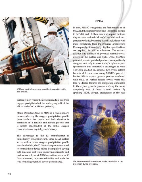
62 A 300mm ingot is loaded onto a cart for transporting to the next process. surface region where the device is made is free from oxygen precipitates but the underlying bulk of the silicon wafer had sufficient gettering. Magic Denuded Zone or MDZ is a revolutionary process whereby the oxygen precipitation profile (near surface free depth and bulk density) is controlled in a reliable and robust process that is nearly independent of the initial oxygen concentration or crystal growth history. The advantage to the IC manufacturer is immediately straightforward. Since MDZ wafers arrive with a robust oxygen precipitation profile template built in, the IC fabrication process required to control these device killers is simplified, saving both time and cost while improving reliability and performance. In short, MDZ saves time, reduces IC fabrication cost, improves reliability, and leads the way for next generation device performance. oPtIa In 1999, MEMC was granted the first patents on its MDZ and the Optia product line. Integrated circuits in the VLSI and ULSI era continue to push limits as they strive to maintain Moore’s Law with each next generation device becoming increasingly dense with more complexity than the previous architecture. Consequently, increasingly tighter specifications are required for silicon substrates. The optimal solution is to eliminate all potential harmful crystal defects in the surface and bulk. Optia, MEMC’s patented premier polished product, was specifically designed not only to meet today’s tighter crystal specification but tomorrow’s challenges as well. The Optia product line resolves two crystal-related harmful defects at once using MEMC’s patented Perfect Silicon crystal growth process combined with MDZ. In Perfect Silicon, crystal voids that lead to device failures are completely eliminated in the crystal growth process, making the wafer completely free of these harmful defects. By applying MDZ, oxygen precipitates in the near The 300mm wafers in carriers are stocked on shelves in the clean room during processing.
MEMC worldwide R&D Cleanroom Lab, St. Peters. surface are eliminated, leaving a deep denuded zone for IC fabrication. Elimination of all crystalrelated harmful defects in the real estate used for IC device fabrication area is an optimal solution for today and future device generations. 300MM waFers In 1991, the push began to develop 300mm wafers. MEMC’s customers, working constantly to maintain their own competitive edge, predicted they could achieve about 2.25 times more devices on each wafer with the transition from a 200mm wafer to a 300mm wafer. While the move to 300mm wafers would entail capital expenditures by the device manufacturers for new equipment and facilities to handle the larger diameter, those costs would not increase in proportion to the surface area, largely because the 300mm wafer meant less wasted silicon near the wafer edge where the rectangular devices meet the curved outer diameter of the wafer. MEMC began producing and selling 300mm wafers by the end of 1995. The shift from 200mm to 300mm wafers again involved subtle evolutionary refinements of the basic manufacturing process. Tighter flatness specifications were achieved by the development of double-sided polishing, which helped to keep the device lines cleaner. This is because the backside of the wafer was polished smooth and no longer had the rough surface composed of pits from etching. The etch pits acted as particle traps and released the particles during wafer processing, causing some contamination of the device lines. In addition, MEMC added edge polishing to the process. This also helped to keep the device lines clean, especially with the advent of immersion lithography in the fabrications. Though edge grinding was introduced in the manufacture of smaller diameter wafers, edge polishing further increased the wafer’s chip resistance. MEMC was already supplying 300mm wafers to many of the twenty-six leading semiconductor device makers worldwide when the first phase of the 300mm research and development line at St. Peters was completed in March of 1997. The line included a full set of innovative equipment to convert 300mmdiameter silicon crystals into 775-micron thick wafers with ultraflat, polished surfaces. In October of 1997, MEMC celebrated the opening of St. Peters’ state-of-the-art large-diameter wafer production facilities. According to then president and COO, Dr. Robert Sandfort, of the more than $600 million in capital investments spent worldwide in 1996, $150 million of it was spent at the St. Peters site. Sources: Electronic News, November 14, 1988 St. Louis Business Journal, April 23, 1990 A Global Company 63
- Page 12 and 13: 12 Float Zone reactors for polysili
- Page 14 and 15: 14 DiD yoU knoW? The Czochralski pr
- Page 16 and 17: 1959 August 6, J. L. Christian, vic
- Page 18 and 19: 18 in hiS oWn WorDS: Dr. roberT WAl
- Page 20 and 21: 20 Dr. Robert Sandfort, who was nam
- Page 22 and 23: 22 Distillation columns at the St.
- Page 24 and 25: 24 business got off to a slow start
- Page 26 and 27: 26 C H A P T E R T H R E E A Second
- Page 28 and 29: 28 1970 The SEMI organization is fo
- Page 30 and 31: 30 wafer lapping, 1975. The Milton
- Page 32 and 33: 32 Zone refiner. 1 st Left to right
- Page 34 and 35: 34 SPArTAnbUrg leArning DiSCovery I
- Page 36 and 37: 36 Mortin Sentman slicing wafers. P
- Page 38 and 39: 38 In 1980, with the basic technolo
- Page 40 and 41: 40 1979 Sony introduces the walkman
- Page 42 and 43: 42 1986 MEMC builds the Utsunomiya,
- Page 44 and 45: 44 Ralph Hartung, vice president, U
- Page 46 and 47: 46 in the past several years, polys
- Page 48 and 49: 48 Above: Epi reactor. Left: Epitax
- Page 50 and 51: 50 Within a year of its merger with
- Page 52 and 53: 1990 Tim Berners-Lee creates the wo
- Page 54 and 55: 54 300mm double-sided polishing.
- Page 56 and 57: 56 MEMC Southwest Groundbreaking Ce
- Page 58 and 59: 58 M E M C A D V E R T I S E M E N
- Page 60 and 61: 60 Dr. roberT fAlSTer: in hiS oWn W
- Page 64 and 65: 64 DiD yoU knoW? In October of 1995
- Page 66 and 67: 66 2002 worldwide semiconductor mat
- Page 68 and 69: 68 Hörde moved from COO to CEO in
- Page 70 and 71: 70 70 MeMC goeS inTo oUTer SPACe! I
- Page 72 and 73: 72 Lifestyles have changed dramatic
- Page 74 and 75: May 2000 MEMC receives the C. Sheld
- Page 76 and 77: 76 The people of MKC celebrate thei
- Page 78 and 79: 78 2009 website www.memc.com percen
- Page 80: 80 Ahmad Chatila, MEMC President an
62<br />
A 300mm ingot is loaded onto a cart for transporting to the<br />
next process.<br />
surface region where the device is made is free from<br />
oxygen precipitates but the underlying bulk of the<br />
silicon wafer had sufficient gettering.<br />
Magic Denuded Zone or MDZ is a revolutionary<br />
process whereby the oxygen precipitation profile<br />
(near surface free depth and bulk density) is<br />
controlled in a reliable and robust process that<br />
is nearly independent of the initial oxygen<br />
concentration or crystal growth history.<br />
The advantage to the IC manufacturer is<br />
immediately straightforward. Since MDZ wafers<br />
arrive with a robust oxygen precipitation profile<br />
template built in, the IC fabrication process required<br />
to control these device killers is simplified, saving<br />
both time and cost while improving reliability and<br />
performance. In short, MDZ saves time, reduces IC<br />
fabrication cost, improves reliability, and leads the<br />
way for next generation device performance.<br />
oPtIa<br />
In 1999, <strong>MEMC</strong> was granted the first patents on its<br />
MDZ and the Optia product line. Integrated circuits<br />
in the VLSI and ULSI era continue to push limits as<br />
they strive to maintain Moore’s Law with each next<br />
generation device becoming increasingly dense with<br />
more complexity than the previous architecture.<br />
Consequently, increasingly tighter specifications<br />
are required for silicon substrates. The optimal<br />
solution is to eliminate all potential harmful crystal<br />
defects in the surface and bulk. Optia, <strong>MEMC</strong>’s<br />
patented premier polished product, was specifically<br />
designed not only to meet today’s tighter crystal<br />
specification but tomorrow’s challenges as well.<br />
The Optia product line resolves two crystal-related<br />
harmful defects at once using <strong>MEMC</strong>’s patented<br />
Perfect Silicon crystal growth process combined<br />
with MDZ. In Perfect Silicon, crystal voids that<br />
lead to device failures are completely eliminated<br />
in the crystal growth process, making the wafer<br />
completely free of these harmful defects. By<br />
applying MDZ, oxygen precipitates in the near<br />
The 300mm wafers in carriers are stocked on shelves in the<br />
clean room during processing.


