BUILDING ON THE PAST, READY FOR THE FUTURE: - MEMC
BUILDING ON THE PAST, READY FOR THE FUTURE: - MEMC BUILDING ON THE PAST, READY FOR THE FUTURE: - MEMC
44 Ralph Hartung, vice president, US Manufacturing. Photo from the early 1980s. Liz Dulick leads a tour of post polishing through final cleaning at the St. Peters plant. An article in the October 1992 edition of Semiconductor International explained the significance of the 200mm diameter wafer to the semiconductor industry: Semiconductor manufacturers are gearing up to use 200mm wafers primarily for high volume, large area circuits such as DRAMs, SRAMs, flash-EPROMs DrAM, SrAM, AnD eProM DRAM or Dynamic Random Access Memory is a type of random access memory that stores each bit of data in a separate capacitor within an integrated circuit. Random access means that locations in the memory can be written to or read from in any order, regardless of the memory location that was last accessed. SRAM or Static Random Access Memory is faster and less power hungry than DRAM. Owing to a more complex internal structure, SRAM is less dense than DRAM and is therefore not used for highcapacity, low-cost applications such as the main memory in personal computers. An EPROM, or Erasable Programmable Read-Only Memory, is a type of memory chip that retains its data when its power supply is switched off. and HDTV related memory. Officials at MEMC Electronic Materials foresee, over the next five years, the sale of 200mm wafers will be increasing by 800 percent. ContInued InnovatIons Up until 1992, the Inner Diameter Saw, or ID saw, was the standard operation for slicing wafers. For the production of 200mm wafers, the move was made toward wire sawing. With wire sawing, one complete ingot is placed in the saw, and a single helical wire makes multiple cuts through the ingot at the same time. Though much faster and more efficient than the ID saw, the potential downside is that if something goes wrong you risk losing the entire ingot. One advantage, however, is that while the diamond ID saw cut was about 350 microns wide, the wire saw is 200 microns wide, creating less waste per cut and more wafers per ingot.
Also notable is the fact that, during this time, the controls of the crystal-growing furnaces were changed to computer-digital systems, giving the operators finer gradations of control. It was one of those strange twists of fate where the silicon wafer MEMC was making was improved through the use of the silicon-based circuits in the computerized control system. headlIne: “Monsanto to sell sIlICon waFer FIrM” Although the front-page article in the November 14, 1988, issue of Electronic News announcing Monsanto’s plans to sell its electronic products division didn’t exactly read like an obituary, for some it felt like one. As the nation’s sole producer of 8” silicon wafers, news of the impending sale sent shockwaves through Silicon Valley, and many feared it was an indication that the United States was losing its technological edge. Worse, the Department of Defense feared that the United States’ security could be jeopardized should silicon wafer production, a critical defense technology, leave the country. While some American companies, including IBM, Texas Instruments, and Motorola, had their own internal wafer production, none of these facilities was large enough to fill the gap should a crisis of national security occur. One Silicon Valley insider was quoted in Electronic News saying, “This is it. It’s all over. Monsanto was the last stand.” Headline announces Monsanto’s intent to sell MEMC. Above: wafer slicer, 2009. Below: This diagram explains both the inner diameter saw and wire sawing of wafers. Great Strides in Technology 45
- Page 1: B u i l d i n g o n t h e p a s t ,
- Page 4 and 5: Copyright © 2009 by MEMC All right
- Page 6 and 7: 6 A C K N O w L E D G M E N T S The
- Page 8 and 9: 8 This is the story about a large c
- Page 10 and 11: 10 The first integrated circuit. Bo
- Page 12 and 13: 12 Float Zone reactors for polysili
- Page 14 and 15: 14 DiD yoU knoW? The Czochralski pr
- Page 16 and 17: 1959 August 6, J. L. Christian, vic
- Page 18 and 19: 18 in hiS oWn WorDS: Dr. roberT WAl
- Page 20 and 21: 20 Dr. Robert Sandfort, who was nam
- Page 22 and 23: 22 Distillation columns at the St.
- Page 24 and 25: 24 business got off to a slow start
- Page 26 and 27: 26 C H A P T E R T H R E E A Second
- Page 28 and 29: 28 1970 The SEMI organization is fo
- Page 30 and 31: 30 wafer lapping, 1975. The Milton
- Page 32 and 33: 32 Zone refiner. 1 st Left to right
- Page 34 and 35: 34 SPArTAnbUrg leArning DiSCovery I
- Page 36 and 37: 36 Mortin Sentman slicing wafers. P
- Page 38 and 39: 38 In 1980, with the basic technolo
- Page 40 and 41: 40 1979 Sony introduces the walkman
- Page 42 and 43: 42 1986 MEMC builds the Utsunomiya,
- Page 46 and 47: 46 in the past several years, polys
- Page 48 and 49: 48 Above: Epi reactor. Left: Epitax
- Page 50 and 51: 50 Within a year of its merger with
- Page 52 and 53: 1990 Tim Berners-Lee creates the wo
- Page 54 and 55: 54 300mm double-sided polishing.
- Page 56 and 57: 56 MEMC Southwest Groundbreaking Ce
- Page 58 and 59: 58 M E M C A D V E R T I S E M E N
- Page 60 and 61: 60 Dr. roberT fAlSTer: in hiS oWn W
- Page 62 and 63: 62 A 300mm ingot is loaded onto a c
- Page 64 and 65: 64 DiD yoU knoW? In October of 1995
- Page 66 and 67: 66 2002 worldwide semiconductor mat
- Page 68 and 69: 68 Hörde moved from COO to CEO in
- Page 70 and 71: 70 70 MeMC goeS inTo oUTer SPACe! I
- Page 72 and 73: 72 Lifestyles have changed dramatic
- Page 74 and 75: May 2000 MEMC receives the C. Sheld
- Page 76 and 77: 76 The people of MKC celebrate thei
- Page 78 and 79: 78 2009 website www.memc.com percen
- Page 80: 80 Ahmad Chatila, MEMC President an
44<br />
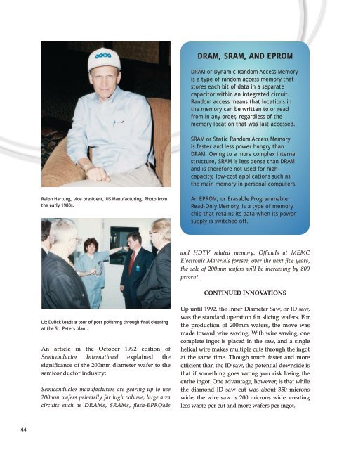
Ralph Hartung, vice president, US Manufacturing. Photo from<br />
the early 1980s.<br />
Liz Dulick leads a tour of post polishing through final cleaning<br />
at the St. Peters plant.<br />
An article in the October 1992 edition of<br />
Semiconductor International explained the<br />
significance of the 200mm diameter wafer to the<br />
semiconductor industry:<br />
Semiconductor manufacturers are gearing up to use<br />
200mm wafers primarily for high volume, large area<br />
circuits such as DRAMs, SRAMs, flash-EPROMs<br />
DrAM, SrAM, AnD eProM<br />
DRAM or Dynamic Random Access Memory<br />
is a type of random access memory that<br />
stores each bit of data in a separate<br />
capacitor within an integrated circuit.<br />
Random access means that locations in<br />
the memory can be written to or read<br />
from in any order, regardless of the<br />
memory location that was last accessed.<br />
SRAM or Static Random Access Memory<br />
is faster and less power hungry than<br />
DRAM. Owing to a more complex internal<br />
structure, SRAM is less dense than DRAM<br />
and is therefore not used for highcapacity,<br />
low-cost applications such as<br />
the main memory in personal computers.<br />
An EPROM, or Erasable Programmable<br />
Read-Only Memory, is a type of memory<br />
chip that retains its data when its power<br />
supply is switched off.<br />
and HDTV related memory. Officials at <strong>MEMC</strong><br />
Electronic Materials foresee, over the next five years,<br />
the sale of 200mm wafers will be increasing by 800<br />
percent.<br />
ContInued InnovatIons<br />
Up until 1992, the Inner Diameter Saw, or ID saw,<br />
was the standard operation for slicing wafers. For<br />
the production of 200mm wafers, the move was<br />
made toward wire sawing. With wire sawing, one<br />
complete ingot is placed in the saw, and a single<br />
helical wire makes multiple cuts through the ingot<br />
at the same time. Though much faster and more<br />
efficient than the ID saw, the potential downside is<br />
that if something goes wrong you risk losing the<br />
entire ingot. One advantage, however, is that while<br />
the diamond ID saw cut was about 350 microns<br />
wide, the wire saw is 200 microns wide, creating<br />
less waste per cut and more wafers per ingot.


