BUILDING ON THE PAST, READY FOR THE FUTURE: - MEMC
BUILDING ON THE PAST, READY FOR THE FUTURE: - MEMC
BUILDING ON THE PAST, READY FOR THE FUTURE: - MEMC

Create successful ePaper yourself
Turn your PDF publications into a flip-book with our unique Google optimized e-Paper software.
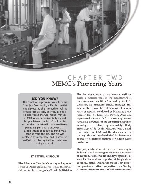
14<br />
DiD yoU knoW?<br />
The Czochralski process takes its name<br />
from Jan Czochralski, a Polish scientist<br />
who discovered this method for pulling<br />
crystal rods as early as 1916. It is said<br />
he discovered the Czochralski method<br />
in 1916 when he accidentally dipped<br />
his pen into a crucible of molten tin<br />
rather than his inkwell. He immediately<br />
pulled his pen out to discover that<br />
a thin thread of solidified metal was<br />
hanging from the nib. The nib was<br />
replaced by a capillary, and Czochralski<br />
verified that the crystallized metal was<br />
a single crystal.<br />
st. Peters, MIssourI<br />
When Monsanto Chemical Company broke ground<br />
for the St. Peters plant in 1959, it was the newest<br />
addition to their Inorganic Chemicals Division.<br />
C H A P T E R T w O<br />
<strong>MEMC</strong>’s Pioneering Years<br />
The plant was to manufacture “ultra-pure silicon<br />
metal, a material used in the manufacture of<br />
transistors and rectifiers,” according to J. L.<br />
Christian, the division’s general manager. This<br />
new venture was the culmination of several<br />
years of research conducted at Monsanto’s two<br />
research labs (St. Louis and Dayton, Ohio) and<br />
represented Monsanto’s first major step toward<br />
supplying products for the emerging electronics<br />
industry. St. Peters, approximately thirty<br />
miles west of St. Louis, Missouri, was a small<br />
rural village in 1959, and the clean air of the<br />
countryside was considered ideal for the extreme<br />
degree of cleanliness required for silicon wafer<br />
production.<br />
The people who stood at the groundbreaking in<br />
St. Peters could not imagine the range and scope<br />
of the products that would one day be possible as<br />
a result of the work accomplished at this plant and<br />
at <strong>MEMC</strong> plants around the world. Few people<br />
can provide a better perspective than Stanley<br />
T. Myers, president and CEO of Semiconductor