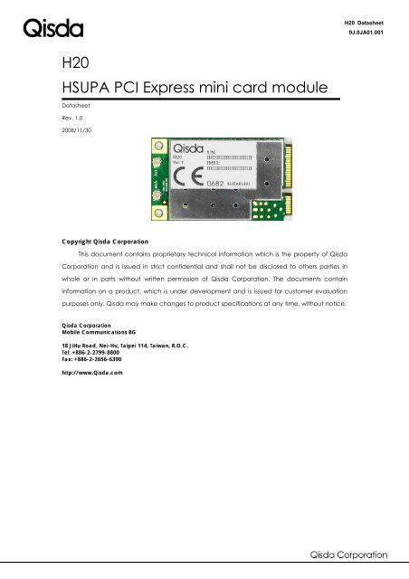
H20 HSUPA PCI Express mini card module - wless.ru
H20 HSUPA PCI Express mini card module - wless.ru
H20 HSUPA PCI Express mini card module - wless.ru
- No tags were found...

You also want an ePaper? Increase the reach of your titles
YUMPU automatically turns print PDFs into web optimized ePapers that Google loves.
HISTORYVersion Date NotesVER: 1.0 2008-NOV-30 FIRST RELEASE
1. INTRODUCTION1.1 DescriptionOverviewThis document describes all the functions, features, and interfaces of the <strong>HSUPA</strong> <strong>PCI</strong><strong>Express</strong> Mini Card Module – <strong>H20</strong> from Qisda. Qisda <strong>H20</strong> <strong>HSUPA</strong> <strong>module</strong> supports Tri-bandWCDMA/HSDPA/<strong>HSUPA</strong> and Quad-band GSM/GPRS/EDGE network connection capability.Qisda <strong>H20</strong> <strong>HSUPA</strong> <strong>card</strong> can provides high speed data connection, the data speed ofdownlink and uplink path is up to 7.2Mbps and 5.76Mbps respectively .Furthermore, users canease to use this <strong>module</strong> by using the “HSPA Modem” application software that we provide forWindows XP and Vista system.With the Qisda <strong>H20</strong> <strong>HSUPA</strong> <strong>module</strong>, devices are enhanced in both functionality andusability based on state of the art wireless technology.1.2 Application DeviceScopeQisda <strong>H20</strong> <strong>module</strong> is a high speed modem <strong>card</strong> with <strong>PCI</strong> <strong>Express</strong> <strong>mini</strong><strong>card</strong> form factorand is focusing on the Notebook, UMPC, MID and other portable device marketing.‣ Notebook‣ Ultra Mobile PC‣ Mobile Internet Device‣ Wireless Router
2. FEATURES2.1 General Characteristics• Bands:Tri Band WCDMA and Quad Band GSMBand TX RXGSM850 824~849 MHz 869~894MHzEGSM900 880~915 MHz 925~960MHzDCS1800 1710~1785MHz 1805~1880MHzPCS1900 1850~1910MHz 1930~1990MHzWCDMA850 824~849 MHz 869~894MHzWCDMA1900 1850~1910MHz 1930~1990MHzWCDMA2100 1920~1980MHz 2110~2170MHz• Support SIM Interface: 1.8V/3V• Form factori. Dimension: 50.95 x 30 x 5.0 mmii.Weight: 12g• PowerOperation Voltage: 3.3V +/- 9%• Power Consumption:Data Mode:Band Typ Max UnitGSM850 / PCL=5 360 390 mAEGSM900 / PCL=5 360 390 mADCS / PCL=0 310 340 mAPCS / PCL=0 310 340 mAWCDMA (all band) 750 820 mAEDGE & GPRS Multislut:GMSK8PSKBand Slot 1 Slot 2 Slot 3 Slot 4 Slot 1 Slot 2 Slot 3 Slot 4GSM850 < 380mA
Sleeping Mode:Typ (Average) Max (Average) UnitGSM / MFRM=2 5 6 mAGSM / MFRM =9 3 4.5 mADCS / MFRM =2 5 6 mADCS / MFRM =9 3.4 5 mAPCS / MFRM =2 5 6 mAPCS / Page frame=9 3.1 4.5 mAWCDMA / DRX=6 (0.64 S) 5.7 5.5 mAWCDMA / DRX=9 (5.12 S) 3.2 4.5 mAShutdown current 0.1 1 uA• Hardware Interface:52 Pins <strong>PCI</strong> <strong>Express</strong> Mini Card connector interface2 RF Antenna Coaxial Connectors• Software Interface:USB driverHSPA Modem software tool.2.2 RF FunctionalitiesMaximum TX PowerThe performance of the transmitter meets test requirement ETSI TS 151 010-1 chapter 13.3 forGSM, chapter 13.17.3 for EDGE and TS 34.121 chapter 5.2&5.4.3 for WCDMA, chapter 5.2A forHSDPA, chapter 5.2B for <strong>HSUPA</strong>.Band Max MinGSM850 33 dBm ±2dBm 5 dBm ±5dBmEGSM 33 dBm ±2dBm 5 dBm ±5dBmDCS 30 dBm ±2dBm 0 dBm ±5dBmPCS 30 dBm ±2dBm 0 dBm ±5dBmGSM850(EDGE) 27 dBm ±3dBm 5 dBm ±5dBmEGSM(EDGE) 27 dBm ±3dBm 5 dBm ±5dBmDCS(EDGE) 26 dBm ±3dBm 2 dBm ±5dBmPCS(EDGE) 26 dBm ±3dBm 2 dBm ±5dBmUMTS-2100 24 dBm +1/-3dBm Less than -50dBmUMTS-1900 24 dBm +1/-3dBm Less than -50dBmUMTS-850 24 dBm +1/-3dBm Less than -50dBm1/15≦βo/βd≦12/15 (HS-DPCCH)24 dBm +1/-3dBm13/15≦βo/βd≦15/8 (HS-DPCCH)23 dBm +2/-3dBm
15/7≦βo/βd≦15/0 (HS-DPCCH)Sub-test 1 (E-DCH)Sub-test 2 (E-DCH)Sub-test 3 (E-DCH)Sub-test 4 (E-DCH)Sub-test 5 (E-DCH)22 dBm +3/-3dBm24 dBm +1.7/-5.2dBm22 dBm +3.7/-5.2dBm23 dBm +2.7/-5.2dBm22 dBm +3.7/-5.2dBm24 dBm +1.7/-5.2dBmParametric PerformanceTests carried out at -20ºC, 25ºC and 60ºC for each voltage 3V, 3.3V and 3.6V. The MeasuredPeak Phase, RMS Phase, frequency error, power level, and static sensitivity meets ETSI TS 151010-1 chapter 13.1 for GSM and TS 34.121 chapter 5.13.1 for WCDMA, chapter 5.13.1A for HSDPABand (GSM) Peak Phase Error RMS Phase ErrorGSM850
ModulationDuplex SpacingFrequency StabilityPower OutputOutput ImpedanceSpurious EmissionEGSM (900 MHz)Frequency RangeChannel SpacingNumber of ChannelsModulationDuplex SpacingFrequency StabilityPower OutputOutput ImpedanceSpurious EmissionDCS (1800 MHz)Frequency RangeChannel SpacingNumber of ChannelsModulationDuplex SpacingFrequency StabilityPower OutputOutput ImpedanceSpurious EmissionPCS (1900 MHz)Frequency RangeChannel SpacingNumber of ChannelsModulationDuplex SpacingFrequency StabilityPower OutputOutput ImpedanceSpurious EmissionWCDMA_IMT (2100 MHz)Frequency RangeChannel RasterNumber of ChannelsModulationDuplex SpacingFrequency StabilityPower OutputOutput ImpedanceSpurious EmissionGMSK / 8-PSK45 MHz+/- 0.1 ppm (Uplink TX)33 dBm Class 8 (2 W peak) – 5 dBm50 Ohm-36 dBm up to 1 GHz (< -30 dBm > 1 GHz)TX 880-915 MHz; RX 925-960 MHz200 KHz124 Carriers x 8 (TDMA)GMSK / 8-PSK45 MHz+/- 0.1 ppm (Uplink TX)33 dBm Class 8 (2 W peak) – 5 dBm50 Ohm-36 dBm up to 1 GHz (< -30 dBm > 1 GHz)TX 1710-1785 MHz; RX 1805-1880 MHz200 KHz374 Carriers x 8 (TDMA)GMSK / 8-PSK95 MHz+/- 0.1 ppm (Uplink TX)30 dBm – 0 dBm50 Ohm-36 dBm up to 1 GHz (< -30 dBm > 1 GHz)Compatible with phase 2 featureTX: 1850~1910MHz; RX: 1930~1990MHz200KHz299 Carriers x 8 (TDMA)GMSK / 8-PSK80 MHz+/- 0.1 ppm (Uplink TX)30 dBm – 0 dBm50 Ohm-36 dBm up to 1 GHz (< -30 dBm > 1 GHz)Compatible with phase 2 featureTX: 1920~1980MHz; RX: 2110~2170MHz200KHz299 Carriers x 8 (TDMA)QPSK190 MHz+/- 0.1 ppm (Uplink TX)24 dBm +1/-3dBm - less than -50dBm50 Ohm-67dBm(925-935MHz);-79dBm(935-960MHz);-71dBm(1805-1880MHz);-60dBm(1845-1880MHz);-41dBm(1885-1920MHz)
WCDMA_PCS (1900 MHz)Frequency RangeChannel RasterNumber of ChannelsModulationDuplex SpacingFrequency StabilityPower OutputOutput ImpedanceSpurious EmissionWCDMA_850 (850 MHz)Frequency RangeChannel RasterNumber of ChannelsModulationDuplex SpacingFrequency StabilityPower OutputOutput ImpedanceSpurious EmissionTX: 1850~1910MHz; RX: 1930~1990MHz200KHz299 Carriers x 8 (TDMA)QPSK80 MHz+/- 0.1 ppm (Uplink TX)24 dBm +1/-3dBm - less than -50dBm50 OhmTX 824-849 MHz; RX 869-894 MHz200KHz299 Carriers x 8 (TDMA)QPSK45 MHz+/- 0.1 ppm (Uplink TX)24 dBm +1/-3dBm - less than -50dBm50 Ohm-60dBm(869-894MHz;1930-1990MHz;2110-2155MHz)GPS performanceCurrent sensitivity is measured to be -154dBm.GSM or WCDMA connection to basic station reduces sensitivity. The sensitivity is measured to be-152dBmWhen the GPS function enable, total current consumption will increase about 138 mA.GPS and Receiver diversity FunctionThe receiver diversity and GPS functionality can not be used simultaneously. So, using GPSactive the <strong>module</strong> will be disable the receiver diversity functionality. When GPS reception isfinished, <strong>module</strong> will be automatic change to receiver diversity mode. For this reason, thesecondary antenna must be designed to support the both GPS and UMTS band frequencyNote:No support active antenna for GPS functionality
3. HARDWARE DESCRIPTION3.1 System InterfaceThe I/O connectors of <strong>H20</strong> <strong>module</strong> are <strong>PCI</strong> EXPRESS MINI CARD and two RF antenna connectors.Table 3-1 summarizes the 25 signals and 18 power lines that are supported by the <strong>PCI</strong> <strong>Express</strong>Mini Card System Interface. Table 3-2 shows the antenna interface.Table 3-1 System InterfaceSignal Group Pin no. DescriptionPower 5 3.3V power sourceGND 13 Return current pathUSB 2 USB serial data interface compliant to the USB 2.0 specificationPERST# 1 Function reset to the <strong>card</strong>W_DISABLE# 1 Shutdown the HSDPA <strong>module</strong>USIM 4 SIM functionLED 1 Status indicatorsPCM 4 PCM interfaceTable 3-2 Antenna interfaceSignal Group Connector no. DescriptionANT 2 Antenna interface
3.2 Functional DiagramQisda <strong>H20</strong> HSPA <strong>PCI</strong> <strong>Express</strong> <strong>mini</strong> <strong>card</strong> Block Diagram<strong>PCI</strong>eBusI/Fx5+3.3VPowerNAND Flash&DDR SDRAM(MCP)1G/512MUART I/F(for GPS)x2USIM I/Fx6Control SignalsStatus IndicatorUSB DATAx2DC/DCConverterNANDInterfacex16x32DDR SDRAMInterface3.6VMobile Station ModemQCT MSM7225USBTransceiverSSBIPower Management UnitQCT PM7540RX IQx2SSBIRX IQx2TX IQx2UMTS TransceiverQCT RTR6285U1900RX SAWU2100RX SAWU850 RXSAWGSM/PCS/DCS RXGSM/PCS/DCS TXUMTS TXU850TX SAWU2100TX SAW850/900SAW1800/1900SAWQuad BandPAPAPAGPSRX SAWQuad Band UMTS RX DRxT/RT/RUMTSRX PRxGSM850 RXGSM900 RXDCS1800 RXPCS1900 RXSWITCHPLEXER850/900 TX(Low Band)1800/1900 TX(High Band)SWITCHPLEXERUMTSDiversityPrimaryAntenna32.768KHzCrystal19.2MHzTCXOU1900TX SAWPAT/RUMTS2100 (Band I)1920 ~ 1980 MHz (UL)2110 ~ 2170 MHz (DL)UMTS1900 (Band II)1850 ~ 1910 MHz (UL)1930 ~ 1990 MHz (DL)UMTS850 (Band V)824 ~ 849 MHz (UL)869 ~ 894 MHz (DL)GSM850824 ~ 849 MHz (UL)869 ~ 894 MHz (DL)GSM900890 ~ 915 MHz (UL)935 ~ 960 MHz (DL)DCS18001710 ~ 1785 MHz (UL)1805 ~ 1880 MHz (DL)PCS19001850 ~ 1910 MHz (UL)1930 ~ 1990 MHz (DL)
3.3 Pin DescriptionPin Signal name Direction Description1 NC No connect2 +3.3Vaux Power 3.3V power source3 NC No connect4 GND Power Return current path5 NC No connect6 NC No connect7 NC No connect8 UIM_PWR Output Power source for the USIM9 GND Power Return current path10 UIM_DATA Input / Output USIM data signal11 NC No connect12 UIM_CLK Output USIM clock signal13 NC No connect14 UIM_RESET Output USIM reset signal15 GND Power Return current path16 NC No connect17 NC No connect18 GND Power Return current path19 NC No connectActive low signal.20 W_DISABLE# InputThis signal is used by the system to shutdownthe HSDPA <strong>module</strong>.21 GND Power Return current path22 PERST# InputActive low signal.Function reset to the <strong>card</strong>.23 NC No connect24 +3.3Vaux Power 3.3V power source25 NC No connect26 GND Power Return current path27 GND Power Return current path28 NC No connect29 GND Power Return current path30 NC No connect31 NC No connect
32 NC No connect33 NC No connect34 GND Power Return current path35 GND Power Return current path36 USB_D- Input / Output USB serial data interface (negative)37 GND Power Return current path38 USB_D+ Input / Output USB serial data interface (postive)39 +3.3Vaux Power 3.3V power source40 GND Power Return current path41 +3.3Vaux Power 3.3V power source42 LED_WWAN# OutputActive low signal.WAN status LED driver.43 GND Power Return current path44 NC No connect45 PCM_CLK Output PCM Clock46 NC No connect47 PCM_DIN Input PCM data input48 NC No connect49 PCM_DOUT Output PCM data output50 GND Power Return current path51 PCM_SYNC Output PCM data strobe52 +3.3Vaux Power 3.3V power source
3.4 Terminal DefinitionRecommend antenna connectHirose Coaxial Connectors
System connectorThe Qisda <strong>H20</strong> <strong>PCI</strong>E <strong>Express</strong> interface compatibility Mini Card Electromechanical SpecificationRevision 1.1.
3.5 Electrical CharacteristicsDC characteristicsPin Function/ Name Direction Parameter Min Typ Max Unit1 NC2 +3.3Vaux Power Power Supply Voltage 3.0 3.3 3.6 V3 NC4 GND Power Ground5 NC6 NC7 NC8 UIM_PWR OutputSupply Voltage 1.5 2.85 3.05 VCurrent 150 mA9 GND Power Ground10 UIM_DATA Input / Output11 NC12 UIM_CLK Output13 NC14 UIM_RESET Output15 GND Power Ground16 NC17 NC18 GND Power Ground19 NC20 W_DISABLE# InputLogic High Input Voltage 0.7VccLogic Low Input Voltage 0.3Vcc VV21 GND Power Ground22 PERST# InputLogic High Input Voltage 0.65VccLogic Low Input Voltage 0.35Vcc VV23 NC24 +3.3Vaux Power Power Supply Voltage 3.0 3.3 3.6 V25 NC26 GND Power Ground27 GND Power Ground28 NC29 GND Power Ground30 NC31 NC
32 NC33 NC34 GND Power Ground35 GND Power Ground36 USB_D- Input / Output Termination Voltage 3.3 V37 GND Power Ground38 USB_D+ Input / Output Termination Voltage 3.3 V39 +3.3Vaux Power Power Supply Voltage 3.0 3.3 3.6 V40 GND Power Ground41 +3.3Vaux Power Power Supply Voltage 3.0 3.3 3.6 V42 LED_WWAN# Output Driver current 10 mA43 GND Power Ground44 NC45 PCM_CLK Output46 NC47 PCM_DIN Input48 NC49 PCM_DOUT Output50 GND Power Ground51 PCM_SYNC Output52 +3.3Vaux Power Power Supply Voltage 3.0 3.3 3.6 V◆ Power Supply:Symbol Parameter Min Typ Max Unit+3.3Vaux Power Supply Voltage 3.0 3.3 3.6 VIsys System Current Consumption 2.5 A※ The <strong>module</strong> draws more than 2.5A peak current while transmitting. Use widetraces for power supply line and compliant with the PCB layout <strong>ru</strong>le.The current rating of component related with the power supply line must betaken into consideration.
◆ Control Interface:․W_DISABLE# :Symbol Parameter Min Max UnitVIH High Level Input Voltage 0.7Vcc VVIL Low Level Input Voltage 0.3Vcc Vtpwron Power-on sequence interval 1.5 secHigh Level: Device Power onLow Level: Device Power off※ W_DISABLE# must stay high at least tpwron to power on the Device.․PERST# :Symbol Parameter Min Max UnitVIH High Level Input Voltage 0.65Vcc VVIL Low Level Input Voltage 0.35Vcc VLow Level: Reset <strong>H20</strong>※ PERST# has internal pull-up resistor.◆ USB Transceiver DC characteristicsThe USB interface is powered from 3.3V power source.Parameter Symbol Min Max UnitInput Levels for Low/Full SpeedHigh VIH 2.0 VLow VIL 0.8 VDifferential Input Sensitivity VDI 0.2 VInput Levels for High SpeedHigh Speed Squelch Detection Threshold VHSSQ 100 150 mVHigh Speed Disconnection DetectionVHSDSC 100 150 mVThresholdOutput Levels for Low/Full SpeedLow VOL 0.0 0.3 VHigh VOH 2.85 3.3 V
Output Levels for High SpeedHigh Speed Idle Level VHSOI -10.0 10.0 mVHigh Speed Data Signaling High VHSOH 360 440 mVHigh Speed Data Signaling Low VHSOL -10.0 10.0 mV◆ USIM InterfaceThe USIM signals are defined on system connector to provide the interface between theremovable User Identity Module. USIM interface usually <strong>ru</strong>n off either 1.8V or 3.0V.Pin Name Direction Description8 UIM_PWR Output Power source for the USIM10 UIM_DATA Input / Output USIM data signal12 UIM_CLK Output USIM clock signal14 UIM_RESET Output USIM reset signalParameter Symbol Min Max UnitLogic High Input Voltage VIH 0.65‧VSIM VSIM +0.3 VLogic Low Input Voltage VIL -0.3 0.35‧VSIM VInput High Leakage Current IIH - 1 uAInput Low Leakage Current IIL -1 - uALogic High Output Voltage VOH VSIM-0.45 VSIM VLogic Low Output Voltage VOL 0 0.45 VHigh-Level, Three-State LeakageCurrentIOZH- 1 uALow-Level, Three-State Leakage Current IOZL -1 - uAType I (8 Pins USIM socket)
Type II (6 Pins USIM socket)◆ Current Driver Interface:Parameter Min Typ Max UnitLED_WWAN 10 mALED Application Circuit:※ Recommend to reserve “Resistor” and “Capacitor” for improve RF wirelessperformance.
◆ PCM InterfaceThe PCM interface <strong>ru</strong>ns at 2.048 MHz and uses 488 ns sync pulse (one 2.048-MHz clock tick),and support linear (16 bits), u-law (8 bits) and a-law (8 bits) format.The PCM_SYNC <strong>ru</strong>ns at 8 KHz with a 50% duty cycle.PCM interface DC characteristics ( Vpcm=2.6V)Parameter Symbol Min Max UnitLogic High Input Voltage VIH 0.65‧Vpcm Vpcm +0.3 VLogic Low Input Voltage VIL -0.3 0.35‧Vpcm VInput High Leakage Current IIH - 1 uAInput Low Leakage Current IIL -1 - uALogic High Output Voltage VOH Vpcm-0.45 Vpcm VLogic Low Output Voltage VOL 0 0.45 VHigh-Level, Three-State LeakageCurrentIOZH- 1 uALow-Level, Three-State Leakage Current IOZL -1 - uA
Parameter Description Min Typ Max Unitt(sync) PCM_SYNC cycle time - 125 - ust(synca) PCM_SYNC asserted time - 488 - nst(syncd) PCM_SYNC de-asserted time - 124.5 - ust(clk) PCM_CLK cycle time - 488 - nst(clkh) PCM_CLK high time - 244 - nst(clkl) PCM_CLK low time - 244 - nst(sync_offset) PCM_SYNC offset time to PCM_CLK falling - 122 - nst(sudin) PCM_DIN setup time to PCM_CLK falling 60 - - nst(hdin) PCM_DIN hold time after PCM_CLK falling 60 - - nst(pdout) Delay from PCM_CLK rising to PCM_DOUT valid - - 60 nst(zdout) Delay from PCM_CLK falling to PCM_DOUT HIGH-Z 5 - 60 ns
3.6 EnvironmentalOperational temperature: -20 ~ +60 ℃Functional temperature: -20 ~ +70 ℃Storage temperature: -40 ~ +85 ℃Note:‣ The maximum case temperature (Tc) of shielding case cover should be under 90 ℃ (@RFTX power = 24dBm) for ensure all of the characteristics of <strong>H20</strong> <strong>module</strong> can be fulfilled theETSI specification.‣
3.7 Physical PackageTop View
Bottom View
Side View
4. SOFTWARE CHARACTERISTICS4.1 Introduction<strong>H20</strong> uses the cutting edge technique of Qualcomm 3.75G wireless communication. It is awireless data <strong>card</strong> product embedded in any host device which has <strong>mini</strong>-<strong>PCI</strong> <strong>Express</strong>interface. The software platform is Qualcomm MSM7225. It uses USB interfaces tocommunicate with PC/NB. The USB interfaces are composed of three parts “NDIS interface”,“AT command Serial COM port” and “Qualcomm Diag COM port”. “Network app” use NDISinterface to transmit Internet data between <strong>H20</strong> device and Host device. PC tool (“SMS,phone book and setting app”) can send the standard AT commands to drive <strong>H20</strong> device by“AT command Serial COM port”. “Qualcomm Diag COM port” interface is used forQualcomm and Qisda Factory tools. We can use this interface to get all device debugmessages and update the firmware of your <strong>H20</strong> device.4.2 Software ArchitectureThe <strong>H20</strong> product high-level software architecture is represented in the following figure:(High Level SoftwareArchitecture)
4.2.1. The first layer is application layer.(Application layer)This layer contains network, SMS, phone book, device setting, Qualcomm and Qisda factorytools. Qisda PC tool provides “network App, SMS App, phone book App and setting App”. Usercan use this tool to surf the Internet and manage SMS messages, contact list, device settings.“Qualcomm and Factory Tools” can support technician to get all debug message from <strong>H20</strong>device.4.2.2. The second layer is USB COM interface layer.(USB COM interface layer)<strong>H20</strong> can support three different USB COM interfaces:• NDIS Interface – This interface is in charge of Internet data transmission between <strong>H20</strong>and Host device.• AT command serial COM port- This a standard modem serial port. It can send/receivethe standard AT commands.• Qualcomm Diag COM port- This is Qualcomm proprietary interface, allDebug/Download tools of Qualcomm and Qisda use this interface to transmit data.4.2.3. The third layer is USB driver layer.(USB driver layer)This layer contains PC USB driver and <strong>H20</strong> firmware USB driver. PC transmits data to <strong>H20</strong> firmwarevia this layer.4.2.4. The fourth layer is RNDIS and SIO layer.(RNDIS and SIO layer)This layer works inside <strong>H20</strong> firmware. RNDIS can process the NDIS data and command which USB
driver and QMI RmNet task transmit. SIO can process the AT and diag command which USBdriver and Data service transmit.4.2.5. The fifth layer is task layer.(Task layer)This layer works inside <strong>H20</strong> firmware. QMI RmNet Task is in charge of NDIS command for networkconnection function. Data Service is in charge of processing all AT commands, including SIM,Diag, Phone book and SMS task.4.3 HSPA Modem ApplicationHSPA Modem Application is PC tool for end user to use. This tool contains four main functions-network, SMS, phone book and setting application.
4.3.1. Network App uses NDIS interface to surf the Internet.4.3.2. Phone Book App is in charge of the contact list, includes New, Edit, Export, Importoperations on your SIM <strong>card</strong>.
4.3.3. SMS App is in charge of SMS message receiving, sending, forward, reply, move, copy,delete, new and backup operations.4.3.4. Setting App includes some device settings about operator network setting and PINcode setting.