ADM485 +5 V Low Power EIA RS-485 Transceiver - ZMiTAC
ADM485 +5 V Low Power EIA RS-485 Transceiver - ZMiTAC
ADM485 +5 V Low Power EIA RS-485 Transceiver - ZMiTAC

You also want an ePaper? Increase the reach of your titles
YUMPU automatically turns print PDFs into web optimized ePapers that Google loves.
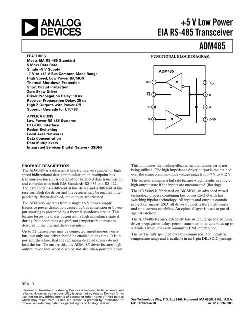
aFEATURESMeets <strong>EIA</strong> <strong>RS</strong>-<strong>485</strong> Standard5 Mb/s Data RateSingle <strong>+5</strong> V Supply–7 V to +12 V Bus Common-Mode RangeHigh Speed, <strong>Low</strong> <strong>Power</strong> BiCMOSThermal Shutdown ProtectionShort Circuit ProtectionZero Skew DriverDriver Propagation Delay: 10 nsReceiver Propagation Delay: 25 nsHigh Z Outputs with <strong>Power</strong> OffSuperior Upgrade for LTC<strong>485</strong>APPLICATIONS<strong>Low</strong> <strong>Power</strong> <strong>RS</strong>-<strong>485</strong> SystemsDTE-DCE InterfacePacket SwitchingLocal Area NetworksData ConcentrationData MultiplexersIntegrated Services Digital Network (ISDN)REDEDIFUNCTIONAL BLOCK DIAGRAM<strong>ADM<strong>485</strong></strong>RO 1 R8 V CC23<strong>+5</strong> V <strong>Low</strong> <strong>Power</strong><strong>EIA</strong> <strong>RS</strong>-<strong>485</strong> <strong>Transceiver</strong><strong>ADM<strong>485</strong></strong>4 D576BAGNDPRODUCT DESCRIPTIONThe <strong>ADM<strong>485</strong></strong> is a differential line transceiver suitable for highspeed bidirectional data communication on multipoint bustransmission lines. It is designed for balanced data transmissionand complies with both <strong>EIA</strong> Standards <strong>RS</strong>-<strong>485</strong> and <strong>RS</strong>-422.The part contains a differential line driver and a differential linereceiver. Both the driver and the receiver may be enabled independently.When disabled, the outputs are tristated.The <strong>ADM<strong>485</strong></strong> operates from a single <strong>+5</strong> V power supply.Excessive power dissipation caused by bus contention or by outputshorting is prevented by a thermal shutdown circuit. Thisfeature forces the driver output into a high impedance state ifduring fault conditions a significant temperature increase isdetected in the internal driver circuitry.Up to 32 transceivers may be connected simultaneously on abus, but only one driver should be enabled at any time. It is important,therefore, that the remaining disabled drivers do notload the bus. To ensure this, the <strong>ADM<strong>485</strong></strong> driver features highoutput impedance when disabled and also when powered down.This minimizes the loading effect when the transceiver is notbeing utilized. The high impedance driver output is maintainedover the entire common-mode voltage range from –7 V to +12 V.The receiver contains a fail safe feature which results in a logichigh output state if the inputs are unconnected (floating).The <strong>ADM<strong>485</strong></strong> is fabricated on BiCMOS, an advanced mixedtechnology process combining low power CMOS with fastswitching bipolar technology. All inputs and outputs containprotection against ESD; all driver outputs feature high sourceand sink current capability. An epitaxial layer is used to guardagainst latch-up.The <strong>ADM<strong>485</strong></strong> features extremely fast switching speeds. Minimaldriver propagation delays permit transmission at data rates up to5 Mbits/s while low skew minimizes EMI interference.The part is fully specified over the commercial and industrialtemperature range and is available in an 8-pin DIL/SOIC package.REV. 0Information furnished by Analog Devices is believed to be accurate andreliable. However, no responsibility is assumed by Analog Devices for itsuse, nor for any infringements of patents or other rights of third partieswhich may result from its use. No license is granted by implication orotherwise under any patent or patent rights of Analog Devices.One Technology Way, P.O. Box 9106, Norwood, MA 02062-9106, U.S.A.Tel: 617/329-4700 Fax: 617/326-8703
<strong>ADM<strong>485</strong></strong>Test CircuitsV CCS2V ODRRV OC0V OR 3VDEABS1C LR LV OUTDE INFigure 1. Driver Voltage Measurement Test CircuitFigure 4. Driver Enable/Disable Test Circuit375ΩAV OD360ΩV TSTBREV OUT375ΩC LFigure 2. Driver Voltage Measurement Test Circuit 2Figure 5. Receiver Propagation Delay Test CircuitAC L1R LDIFFCBL2Figure 3. Driver Propagation Delay Test Circuit+1.5VV CCS1R LS2–1.5VREC LV OUTRE INFigure 6. Receiver Enable/Disable Test CircuitSwitching Characteristics3V1.5V 1.5V0VT PLHA–B0V0VT PHLBAVO0V–VOVO1/2VO90% POINT10% POINTT RT SKEWT SKEW90% POINT10% POINTFigure 7. Driver Propagation Delay, Rise/Fall TimingDE 1.5V1.5VT LZT F3V0VRORET T PLHPHLV OH1.5V 1.5VV OLFigure 9. Receiver Propagation Delay3V1.5V 1.5V0VT T ZL LZ1.5VT ZL2.3VA, BV OL+ 0.5VV OLRO/P LOWV OL+ 0.5VV OLT ZHT HZT ZHT HZA, B2.3VV OH– 0.5VV OHR1.5VO/P HIGHV OH– 0.5VV OHFigure 8. Driver Enable/Disable Timing0V0VFigure 10. Receiver Enable/Disable Timing–4–REV. 0
OUTPUT CURRENT – mAOUTPUT CURRENT – mASUPPLY CURRENT – mAOUTPUT VOLTAGE – VoltsOUTPUT CURRENT – mADIFFERENTIAL VOLTAGE – VoltsOUTPUT CURRENT – mAOUTPUT CURRENT – mAOUTPUT VOLTAGE – VoltsTypical Performance Characteristics–<strong>ADM<strong>485</strong></strong>40363228242016128400.00.5 1.0 1.5OUTPUT VOLTAGE – VoltsFigure 11. Receiver Output <strong>Low</strong>Voltage vs. Output Current2.00–2–4–6–8–10–12–14–16–18–203.54.04.5OUTPUT VOLTAGE – VoltsFigure 12. Receiver Output HighVoltage vs. Output Current5.05.04.94.84.74.64.5–50–25I = 8mA0 25 50 75TEMPERATURE – °C100Figure 13. Receiver Output HighVoltage vs. Temperature1250.4962.40.3I = 8mA8472602.30.20.1–50 –25 0 25 50 75 100 125TEMPERATURE – °CFigure 14. Receiver Output <strong>Low</strong>Voltage vs. Temperature48362412001 2 3OUTPUT VOLTAGE – VoltsFigure 15. Driver Differential OutputVoltage vs. Output Current42.22.12.0–50 –25 0 25 50 75 100 125TEMPERATURE – °CFigure 16. Driver Differential OutputVoltage vs. Temperature, R L = 54 Ω10001.00908070–10–20–300.950.90DRIVER ENABLED60–400.8550–500.80403020–60–70–800.750.70DRIVER DISABLED10–900.65001 2 3OUTPUT VOLTAGE – Volts4–10001 2 3 4OUTPUT VOLTAGE – Volts50.60–50–250 25 50 75TEMPERATURE – °C100125Figure 17. Driver Output <strong>Low</strong>Voltage vs. Output CurrentFigure 18. Driver Output HighVoltage vs. Output CurrentFigure 19. Supply Current vs.TemperatureREV. 0 –5–
TIME – nsTIME – ns<strong>ADM<strong>485</strong></strong>–Typical Performance Characteristics51.0430.90.8100900.720.610.5100%0–50–250 25 50 75TEMPERATURE – °C100Figure 20. Receiver t PLH –t PHL , vs.Temperature1250.4–50 –25 0 25 50 75 100TEMPERATURE – °CFigure 21. Driver Skew vs.Temperature1251V1V5nsFigure 22. Unloaded DriverDifferential Outputs1001001009090901010100%0%0%500mV500mV5ns1V1V5 5 10nsH O1V1V5 5 10nsH OFigure 23. Loaded DriverDifferential OutputsFigure 24. Driver/Receiver PropagationDelays <strong>Low</strong> to HighFigure 25. Driver/Receiver PropagationDelays High to <strong>Low</strong>RTRTDDRRDRDRFigure 26. Typical <strong>RS</strong>-<strong>485</strong> Network–6–REV. 0
<strong>ADM<strong>485</strong></strong>APPLICATIONS INFORMATIONDifferential Data TransmissionDifferential data transmission is used to reliably transmit data athigh rates over long distances and through noisy environments.Differential transmission nullifies the effects of ground shiftsand noise signals which appear as common-mode voltageson the line. There are two main standards approved by theElectronics Industries Association (<strong>EIA</strong>) which specify the electricalcharacteristics of transceivers used in differential datatransmission.The <strong>RS</strong>-422 standard specifies data rates up to 10 MBaud andline lengths up to 4000 ft. A single driver can drive a transmissionline with up to 10 receivers.In order to cater for true multipoint communications, the<strong>RS</strong>-<strong>485</strong> standard was defined. This standard meets or exceedsall the requirements of <strong>RS</strong>-422 but also allows for up to 32drivers and 32 receivers to be connected to a single bus. Anextended common-mode range of –7 V to +12 V is defined. Themost significant difference between <strong>RS</strong>-422 and <strong>RS</strong>-<strong>485</strong> is thefact that the drivers may be disabled thereby allowing more thanone (32 in fact) to be connected to a single line. Only one drivershould be enabled at time, but the <strong>RS</strong>-<strong>485</strong> standard containsadditional specifications to guarantee device safety in the eventof line contention.Cable and Data RateThe transmission line of choice for <strong>RS</strong>-<strong>485</strong> communications is atwisted pair. Twisted pair cable tends to cancel common-modenoise and also causes cancellation of the magnetic fields generatedby the current flowing through each wire, thereby, reducingthe effective inductance of the pair.The <strong>ADM<strong>485</strong></strong> is designed for bidirectional data communicationson multipoint transmission lines. A typical applicationshowing a multipoint transmission network is illustrated inFigure 26. An <strong>RS</strong>-<strong>485</strong> transmission line can have as many as32 transceivers on the bus. Only one driver can transmitat a particular time but multiple receivers may be enabledsimultaneously.As with any transmission line, it is important that reflections areminimized. This may be achieved by terminating the extremeends of the line using resistors equal to the characteristic impedanceof the line. Stub lengths of the main line should also bekept as short as possible. A properly terminated transmissionline appears purely resistive to the driver.Thermal ShutdownThe <strong>ADM<strong>485</strong></strong> contains thermal shutdown circuitry which protectsthe part from excessive power dissipation during fault conditions.Shorting the driver outputs to a low impedance sourcecan result in high driver currents. The thermal sensing circuitrydetects the increase in die temperature and disables the driveroutputs. The thermal sensing circuitry is designed to disable thedriver outputs when a die temperature of 150°C is reached. Asthe device cools, the drivers are reenabled at 140°C.Propagation DelayThe <strong>ADM<strong>485</strong></strong> features very low propagation delay ensuringmaximum baud rate operation. The driver is well balanced ensuringdistortion free transmission.Another important specification is a measure of the skew betweenthe complementary outputs. Excessive skew impairs thenoise immunity of the system and increases the amount of electromagneticinterference (EMI).Receiver Open-Circuit Fail SafeThe receiver input includes a fail-safe feature which guaranteesa logic high on the receiver when the inputs are open circuit orfloating.Table III. Comparison of <strong>RS</strong>-422 and <strong>RS</strong>-<strong>485</strong> Interface StandardsSpecification <strong>RS</strong>-422 <strong>RS</strong>-<strong>485</strong>Transmission Type Differential DifferentialMaximum Cable Length 4000 ft. 4000 ft.Minimum Driver Output Voltage ±2 V ±1.5 VDriver Load Impedance 100 Ω 54 ΩReceiver Input Resistance 4 kΩ min 12 kΩ minReceiver Input Sensitivity ±200 mV ±200 mVReceiver Input Voltage Range –7 V to +7 V –7 V to +12 VNo of Drivers/Receivers Per Line 1/10 32/32REV. 0 –7–
<strong>ADM<strong>485</strong></strong>OUTLINE DIMENSIONSDimensions shown in inches and (mm).8-Lead SOIC (R-8)PIN 181540.1574 (4.00)0.1497 (3.80)0.2440 (6.20)0.2284 (5.80)C1817–18–7/930.0098 (0.25)0.0040 (0.10)0.1968 (5.00)0.1890 (4.80)0.0500(1.27)BSC0.0192 (0.49)0.0138 (0.35)0.102 (2.59)0.094 (2.39)0.0098 (0.25)0.0075 (0.19)8°0°0.0196 (0.50)0.0099 (0.25) x 45°0.0500 (1.27)0.0160 (0.41)8-Pin Plastic DIP (N-8)85PIN 10.280 (7.11)0.240 (6.10)140.430 (10.92)0.348 (8.84)0.325 (8.25)0.300 (7.62)0.210(5.33)MAX0.060 (1.52)0.015 (0.38)0.195 (4.95)0.115 (2.93)0.160 (4.06)0.115 (2.93)0.130(3.30)MIN0.015 (0.381)0.008 (0.204)0.022 (0.558)0.014 (0.356)0.100(2.54)BSC0.070 (1.77)0.045 (1.15)SEATINGPLANE8-Pin Cerdip (Q-8)0.005 (0.13) MIN 0.055 (1.4) MAXPIN 10.200(5.08)MAX0.200 (5.08)0.125 (3.18)810.023 (0.58)0.014 (0.36)0.405 (10.29) MAX0.100(2.54)BSC540.070 (1.78)0.030 (0.76)0.310 (7.87)0.220 (5.59)0.060 (1.52)0.015 (0.38)0.150(3.81)MINSEATINGPLANE0.320 (8.13)0.290 (7.37)0.015 (0.38)0.008 (0.20)15°0°PRINTED IN U.S.A.–8–REV. 0