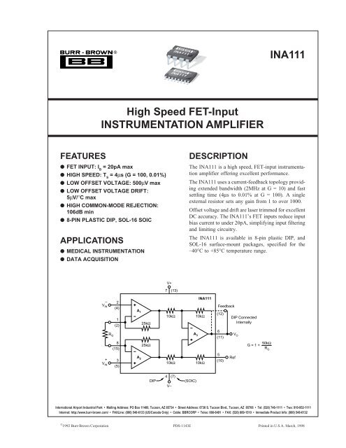
INA111 High Speed FET-Input INSTRUMENTATION AMPLIFIER
INA111 High Speed FET-Input INSTRUMENTATION AMPLIFIER
INA111 High Speed FET-Input INSTRUMENTATION AMPLIFIER
- No tags were found...

You also want an ePaper? Increase the reach of your titles
YUMPU automatically turns print PDFs into web optimized ePapers that Google loves.
®<strong>INA111</strong><strong>INA111</strong><strong>INA111</strong><strong>High</strong> <strong>Speed</strong> <strong>FET</strong>-<strong>Input</strong><strong>INSTRUMENTATION</strong> <strong>AMPLIFIER</strong>FEATURES● <strong>FET</strong> INPUT: I B= 20pA max● HIGH SPEED: T S= 4µs (G = 100, 0.01%)● LOW OFFSET VOLTAGE: 500µV max● LOW OFFSET VOLTAGE DRIFT:5µV/°C max● HIGH COMMON-MODE REJECTION:106dB min● 8-PIN PLASTIC DIP, SOL-16 SOICAPPLICATIONS● MEDICAL <strong>INSTRUMENTATION</strong>● DATA ACQUISITIONDESCRIPTIONThe <strong>INA111</strong> is a high speed, <strong>FET</strong>-input instrumentationamplifier offering excellent performance.The <strong>INA111</strong> uses a current-feedback topology providingextended bandwidth (2MHz at G = 10) and fastsettling time (4µs to 0.01% at G = 100). A singleexternal resistor sets any gain from 1 to over 1000.Offset voltage and drift are laser trimmed for excellentDC accuracy. The <strong>INA111</strong>’s <strong>FET</strong> inputs reduce inputbias current to under 20pA, simplifying input filteringand limiting circuitry.The <strong>INA111</strong> is available in 8-pin plastic DIP, andSOL-16 surface-mount packages, specified for the–40°C to +85°C temperature range.V+7 (13)<strong>INA111</strong>– 2V IN(4)FeedbackA 1(12)10kΩ10kΩ125kΩ(2)6R G A 3 V O(11)825kΩ(15)5A 2 Ref+ 3(10)V IN10kΩ10kΩ(5)DIP ConnectedInternallyG = 1 + 50kΩR GDIP4V–(7)(SOIC)International Airport Industrial Park • Mailing Address: PO Box 11400, Tucson, AZ 85734 • Street Address: 6730 S. Tucson Blvd., Tucson, AZ 85706 • Tel: (520) 746-1111 • Twx: 910-952-1111Internet: http://www.burr-brown.com/ • FAXLine: (800) 548-6133 (US/Canada Only) • Cable: BBRCORP • Telex: 066-6491 • FAX: (520) 889-1510 • Immediate Product Info: (800) 548-61321<strong>INA111</strong>© 1992 Burr-Brown Corporation PDS-1143E Printed in U.S.A. March, 1998®
SPECIFICATIONSELECTRICALAt T A = +25°C, V S = ±15V, R L = 2kΩ, unless otherwise noted.<strong>INA111</strong>BP, BU<strong>INA111</strong>AP, AUPARAMETER CONDITIONS MIN TYP MAX MIN TYP MAX UNITSINPUTOffset Voltage, RTIInitial T A = +25°C ±100 ± 500/G ±500 ± 2000/G ±200 ± 500/G ±1000 ± 5000/G µVvs Temperature T A = T MIN to T MAX ±2 ± 10/G ±5 ± 100/G ±2 ± 20/G ±10 ± 100/G µV/°Cvs Power Supply V S = ±6V to ±18V 2 +10/G 30 + 100/G ✻ ✻ µV/VImpedance, Differential 10 12 || 6 ✻ Ω || pFCommon-Mode 10 12 || 3 ✻ Ω || pF<strong>Input</strong> Common-Mode Range V DIFF = 0V ±10 ±12 ✻ ✻ VCommon-Mode Rejection V CM = ±10V, ∆R S = 1kΩG = 1 80 90 75 ✻ dBG = 10 96 110 90 ✻ dBG = 100 106 115 100 ✻ dBG = 1000 106 115 100 ✻ dBBIAS CURRENT ±2 ±20 ✻ ✻ pAOFFSET CURRENT ±0.1 ±10 ✻ ✻ pANOISE VOLTAGE, RTI G = 1000, R S = 0Ωf = 100Hz 13 ✻ nV/√Hzf = 1kHz 10 ✻ nV/√Hzf = 10kHz 10 ✻ nV/√Hzf B = 0.1Hz to 10Hz 1 ✻ µVp-pNoise Currentf = 10kHz 0.8 ✻ fA/√HzGAINGain Equation 1 + (50kΩ/R G ) ✻ V/VRange of Gain 1 10000 ✻ ✻ V/VGain Error G = 1, R L = 10kΩ ±0.01 ±0.02 ✻ 0.05 %G = 10, R L = 10kΩ ±0.1 ±0.5 ✻ ✻ %G = 100, R L = 10kΩ ±0.15 ±0.5 ✻ ±0.7 %G = 1000, R L = 10kΩ ±0.25 ±1 ✻ ±2 %Gain vs Temperature G = 1 ±1 ±10 ✻ ✻ ppm/°C50kΩ Resistance (1) ±25 ±100 ✻ ✻ ppm/°CNonlinearity G = 1 ±0.0005 ±0.005 ✻ ✻ % of FSRG = 10 ±0.001 ±0.005 ✻ ±0.01 % of FSRG = 100 ±0.001 ±0.005 ✻ ±0.01 % of FSRG = 1000 ±0.005 ±0.02 ✻ ±0.04 % of FSROUTPUTVoltage I O = 5mA, T MIN to T MAX ±11 ±12.7 ✻ ✻ VLoad Capacitance Stability 1000 ✻ pFShort Circuit Current +30/–25 ✻ mAFREQUENCY RESPONSEBandwidth, –3dB G = 1 2 ✻ MHzG = 10 2 ✻ MHzG = 100 450 ✻ kHzG = 1000 50 ✻ kHzSlew Rate V O = ±10V, G = 2 to 100 17 ✻ V/µsSettling Time, 0.01% G = 1 2 ✻ µsG = 10 2 ✻ µsG = 100 4 ✻ µsG = 1000 30 ✻ µsOverload Recovery 50% Overdrive 1 ✻ µsPOWER SUPPLYVoltage Range ±6 ±15 ±18 ✻ ✻ ✻ VCurrent V IN = 0V ±3.3 ±4.5 ✻ ✻ mATEMPERATURE RANGESpecification –40 85 ✻ ✻ °COperating –40 125 ✻ ✻ °Cθ JA 100 ✻ °C/W✻ Specification same as <strong>INA111</strong>BP.NOTE: (1) Temperature coefficient of the “50kΩ” term in the gain equation.The information provided herein is believed to be reliable; however, BURR-BROWN assumes no responsibility for inaccuracies or omissions. BURR-BROWN assumesno responsibility for the use of this information, and all use of such information shall be entirely at the user’s own risk. Prices and specifications are subject to changewithout notice. No patent rights or licenses to any of the circuits described herein are implied or granted to any third party. BURR-BROWN does not authorize or warrantany BURR-BROWN product for use in life support devices and/or systems.®<strong>INA111</strong> 2
PIN CONFIGURATIONSTop ViewR G 1V – IN 2V + IN 3V– 4Top ViewDIP8 R G7 V+6 V O5 RefSOL-16 Surface MountELECTROSTATICDISCHARGE SENSITIVITYThis integrated circuit can be damaged by ESD. Burr-Brownrecommends that all integrated circuits be handled with appropriateprecautions. Failure to observe proper handling andinstallation procedures can cause damage.ESD damage can range from subtle performance degradationto complete device failure. Precision integrated circuits maybe more susceptible to damage because very small parametricchanges could cause the device not to meet its publishedspecifications.NCR GNCV – INV + IN123451615141312NCR GNCV+FeedbackORDERING INFORMATIONPRODUCT PACKAGE TEMPERATURE RANGE<strong>INA111</strong>AP 8-Pin Plastic DIP –40°C to +85°C<strong>INA111</strong>BP 8-Pin Plastic DIP –40°C to +85°C<strong>INA111</strong>AU SOL-16 Surface-Mount –40°C to +85°C<strong>INA111</strong>BU SOL-16 Surface-Mount –40°C to +85°CNCV–671110V ORefPACKAGE INFORMATIONNC8ABSOLUTE MAXIMUM RATINGS (1)Supply Voltage .................................................................................. ±18V<strong>Input</strong> Voltage Range .......................................... (V–) –0.7V to (V+) +15VOutput Short-Circuit (to ground) .............................................. ContinuousOperating Temperature ................................................. –40°C to +125°CStorage Temperature ..................................................... –40°C to +125°CJunction Temperature .................................................................... +150°CLead Temperature (soldering, 10s) ............................................... +300°C9NCPACKAGE DRAWINGPRODUCT PACKAGE NUMBER (1)<strong>INA111</strong>AP 8-Pin Plastic DIP 006<strong>INA111</strong>BP 8-Pin Plastic DIP 006<strong>INA111</strong>AU 16-Pin Surface Mount 211<strong>INA111</strong>BU 16-Pin Surface Mount 211NOTE: (1) For detailed drawing and dimension table, please see end of datasheet, or Appendix C of Burr-Brown IC Data Book.NOTE: Stresses above these ratings may cause permanent damage.3<strong>INA111</strong>®
TYPICAL PERFORMANCE CURVESAt T A = +25°C, V S = ±15V, unless otherwise noted.10kGAIN vs FREQUENCY120COMMON-MODE REJECTION vs FREQUENCYGain (V/V)1k100101G = 1kG = 100G = 10G = 10.11k 10k 100k 1M 10MFrequency (Hz)Common-Mode Rejection (dB)10080G = 1k60G = 10040G = 1020G = 1010 100 1k 10k 100k 1MFrequency (Hz)Common-Mode Voltage (V)151050–5–10INPUT COMMON-MODE VOLTAGE RANGEvs OUTPUT VOLTAGELimited by A 1+ Output SwingLimited by A 2– Output Swing–V D/2+–V D/2+V CMA 3 – OutputSwing Limit(Any Gain)A 3 + OutputSwing Limit–15–15 –10 –5 0 5 10 15Output Voltage (V)Limited by A 2+ Output SwingV OLimited by A 1– Output SwingPower Supply Rejection (dB)12010080604020POWER SUPPLY REJECTION vs FREQUENCY010 100 1k 10k 100k 1MFrequency (Hz)G = 1kG = 100G = 10G = 11kINPUT-REFERRED NOISE VOLTAGE vs FREQUENCY100SETTLING TIME vs GAIN<strong>Input</strong>-Referred Noise Voltage (nV/√Hz)10010G = 1G = 10G = 100, 1kSettling Time (µs)100.01%0.1%11 10 100 1k 10kFrequency (Hz)11 10 100 1000Gain (V/V)®<strong>INA111</strong> 4
TYPICAL PERFORMANCE CURVES (CONT)At T A = +25°C, V S = ±15V, unless otherwise noted.75OFFSET VOLTAGE WARM-UP vs TIME30010nINPUT BIAS CURRENT vs TEMPERATUREI bReferred-to-<strong>Input</strong> V OS Change (µV)50250–25–50G ≥ 10G = 12001000–100–200Referred-to-<strong>Input</strong> V OS Change (µV)<strong>Input</strong> Bias Current (A)1n100p10p1p0.1pI OS–750 1 2 3 4 5Time From Power Supply Turn-On (Minutes)–3000.01p–75 –50 –25 0 25 50 75 100 125Temperature (°C)<strong>Input</strong> Bias Current (A)–10m–1m–100µ–15.7VINPUT BIAS CURRENTvs DIFFERENTIAL INPUT VOLTAGE–10µG = 1 G = 10 G = 100 G = 1k+1pG = 10G = 1+10pG = 1k G = 100+15.7V+100p–20 –15 –10 –5 0 5 10 15 20Differential Overload Voltage (V)NOTE: One input grounded.<strong>Input</strong> Bias Current (A)–10m–1m–100µ–10µ+1pINPUT BIAS CURRENTvs COMMON-MODE INPUT VOLTAGE–15.7VCommon-Mode Voltage (V)+15.7V+10p–20 –15 –10 –5 0 5 10 15 2030MAXIMUM OUTPUT VOLTAGE SWING vs FREQUENCY50OUTPUT CURRENT LIMIT vs TEMPERATUREPeak-to-Peak Amplitude (V)252015105Short-Circuit Current (mA)40302010–I CL+I CL01k 10k 100k 1M 10MFrequency (Hz)0–75 –50 –25 0 25 50 75 100 125Temperature (°C)5<strong>INA111</strong>®
TYPICAL PERFORMANCE CURVES (CONT)At T A = +25°C, V S = ±15V, unless otherwise noted.Quiescent Current (mA)3.53.43.33.23.1QUIESCENT CURRENT vs TEMPERATURETHD + N (%)10.10.010.001G = 1kG = 100G = 10TOTAL HARMONIC DISTORTION + NOISEvs FREQUENCYV O = 3Vrms, R L = 2kΩMeasurement BW = 80kHzSingle-Ended Drive G = 1Differential Drive G = 13.0–75 –50 –25 0 25 50 75 100 125Temperature (°C)0.000120 100 1k 10k 20kFrequency (Hz)LARGE SIGNAL RESPONSE, G = 100SMALL SIGNAL RESPONSE, G = 1+10+0.100–0.1–10010 20Time (µs)010 20Time (µs)LARGE SIGNAL RESPONSE, G = 100SMALL SIGNAL RESPONSE, G = 1+10+0.100–10–0.1010 20Time (µs)010 20Time (µs)®<strong>INA111</strong> 6
APPLICATION INFORMATIONFigure 1 shows the basic connections required for operationof the <strong>INA111</strong>. Applications with noisy or high impedancepower supplies may require decoupling capacitors close tothe device pins as shown.The output is referred to the output reference (Ref) terminalwhich is normally grounded. This must be a low-impedanceconnection to assure good common-mode rejection. A resistanceof 2Ω in series with the Ref pin will cause a typicaldevice with 90dB CMR to degrade to approximately 80dBCMR (G = 1).SETTING THE GAINGain of the <strong>INA111</strong> is set by connecting a single externalresistor, R G :G = 1 + 50kΩR G(1)Commonly used gains and resistor values are shown inFigure 1.The 50kΩ term in equation 1 comes from the sum of the twointernal feedback resistors. These are on-chip metal filmresistors which are laser trimmed to accurate absolute values.The accuracy and temperature coefficient of theseresistors are included in the gain accuracy and drift specificationsof the <strong>INA111</strong>.The stability and temperature drift of the external gainsetting resistor, R G , also affects gain. R G ’s contribution togain accuracy and drift can be directly inferred from the gainequation (1). Low resistor values required for high gain canmake wiring resistance important. Sockets add to the wiringresistance, which will contribute additional gain error (possiblyan unstable gain error) in gains of approximately 100or greater.DYNAMIC PERFORMANCEThe typical performance curve “Gain vs Frequency” showsthat the <strong>INA111</strong> achieves wide bandwidth over a wide rangeof gain. This is due to the current-feedback topology of the<strong>INA111</strong>. Settling time also remains excellent over widegains.V+0.1µFPin numbers arefor DIP package.7– 2<strong>INA111</strong>V INA 110kΩ10kΩ125kΩ6R G A 3825kΩ5A+23RefV IN10kΩ10kΩ+ –V O = G • (V IN – V IN )G = 1 + 50kΩR GLoad+V O–40.1µFDESIRED R GNEAREST 1% R GGAIN (Ω) (Ω)1 No Connection No Connection2 50.00k 49.9k5 12.50k 12.4k10 5.556k 5.62k20 2.632k 2.61k50 1.02k 1.02k100 505.1 511200 251.3 249500 100.2 1001000 50.05 49.92000 25.01 24.95000 10.00 1010000 5.001 4.99V–V IN–V IN+Also drawn in simplified form:R G <strong>INA111</strong> V ORefFIGURE 1. Basic Connections7<strong>INA111</strong>®
The <strong>INA111</strong> exhibits approximately 6dB rise in gain at2MHz in unity gain. This is a result of its current-feedbacktopology and is not an indication of instability. Unlike an opamp with poor phase margin, the rise in response is apredictable +6dB/octave due to a response zero. A simplepole at 700kHz or lower will produce a flat passbandresponse (see <strong>Input</strong> Filtering).The <strong>INA111</strong> provides excellent rejection of high frequencycommon-mode signals. The typical performance curve,“Common-Mode Rejection vs Frequency” shows this behavior.If the inputs are not properly balanced, however,common-mode signals can be converted to differential signals.Run the V IN and V IN connections directly adjacent each+ –other, from the source signal all the way to the input pins. Ifpossible use a ground plane under both input traces. Avoidrunning other potentially noisy lines near the inputs.NOISE AND ACCURACY PERFORMANCEThe <strong>INA111</strong>’s <strong>FET</strong> input circuitry provides low input biascurrent and high speed. It achieves lower noise and higheraccuracy with high impedance sources. With source impedancesof 2kΩ to 50kΩ the INA114 may provide lower offsetvoltage and drift. For very low source impedance (≤1kΩ),the INA103 may provide improved accuracy and lowernoise.INPUT BIAS CURRENT RETURN PATHThe input impedance of the <strong>INA111</strong> is extremely high—approximately 10 12 Ω. However, a path must be provided forthe input bias current of both inputs. This input bias currentis typically less than 10pA. <strong>High</strong> input impedance meansthat this input bias current changes very little with varyinginput voltage.<strong>Input</strong> circuitry must provide a path for this input bias currentif the <strong>INA111</strong> is to operate properly. Figure 3 shows variousprovisions for an input bias current path. Without a biascurrent return path, the inputs will float to a potential whichexceeds the common-mode range of the <strong>INA111</strong> and theinput amplifiers will saturate.If the differential source resistance is low, the bias currentreturn path can be connected to one input (see the thermocoupleexample in Figure 3). With higher source impedance,using two resistors provides a balanced input with possibleadvantages of lower input offset voltage due to bias currentand better high-frequency common-mode rejection.Crystal orCeramicTransducer<strong>INA111</strong>OFFSET TRIMMINGThe <strong>INA111</strong> is laser trimmed for low offset voltage anddrift. Most applications require no external offset adjustment.Figure 2 shows an optional circuit for trimming theoutput offset voltage. The voltage applied to Ref terminal issummed at the output. Low impedance must be maintainedat this node to assure good common-mode rejection. The opamp shown maintains low output impedance at high frequency.Trim circuits with higher source impedance shouldbe buffered with an op amp follower circuit to assure lowimpedance on the Ref pin.Thermocouple1MΩ10kΩ1MΩ<strong>INA111</strong><strong>INA111</strong>–V INR G+V IN<strong>INA111</strong>RefV OV+100µA1/2 REF200Center-tap providesbias current return.OPA177±10mVAdjustment RangeNOTE: (1) For wider trim range requiredin high gains, scale resistor values larger10kΩ (1)100Ω (1)100Ω (1)FIGURE 2. Optional Trimming of Output Offset Voltage.V–100µA1/2 REF200FIGURE 3. Providing an <strong>Input</strong> Common-Mode Current Path.INPUT COMMON-MODE RANGEThe linear common-mode range of the input op amps of the<strong>INA111</strong> is approximately ±12V (or 3V from the powersupplies). As the output voltage increases, however, thelinear input range will be limited by the output voltage swingof the input amplifiers, A 1 and A 2 . The common-mode rangeis related to the output voltage of the complete amplifier—see performance curve “<strong>Input</strong> Common-Mode Range vsOutput Voltage”.®<strong>INA111</strong> 8
A combination of common-mode and differential inputvoltage can cause the output of A 1 or A 2 to saturate. Figure4 shows the output voltage swing of A 1 and A 2 expressed interms of a common-mode and differential input voltages.For applications where input common-mode range must bemaximized, limit the output voltage swing by connecting the<strong>INA111</strong> in a lower gain (see performance curve “<strong>Input</strong>Common-Mode Voltage Range vs Output Voltage”). Ifnecessary, add gain after the <strong>INA111</strong> to increase the voltageswing.<strong>Input</strong>-overload often produces an output voltage that appearsnormal. For example, consider an input voltage of +14V onone input and +15V on the other input will obviously exceedthe linear common-mode range of both input amplifiers.Since both input amplifiers are saturated to the nearly thesame output voltage limit, the difference voltage measuredby the output amplifier will be near zero. The output of the<strong>INA111</strong> will be near 0V even though both inputs areoverloaded.INPUT PROTECTION<strong>Input</strong>s of the <strong>INA111</strong> are protected for input voltages from0.7V below the negative supply to 15V above the positivepower supply voltages. If the input current is limited to lessthan 1mA, clamp diodes are not required; internal junctionswill clamp the input voltage to safe levels. If the input sourcecan supply more than 1mA, use external clamp diodes asshown in Figure 5. The source current can be limited withseries resistors R 1 and R 2 as shown. Resistor values greaterthan 10kΩ will contribute noise to the circuit.A diode formed with a 2N4117A transistor as shown inFigure 5 assures low leakage. Common signal diodes such asthe 1N4148 may have leakage currents far greater than theinput bias current of the <strong>INA111</strong> and are usually sensitive tolight.INPUT FILTERINGThe <strong>INA111</strong>’s <strong>FET</strong> input allows use of an R/C input filterwithout creating large offsets due to input bias current.Figure 6 shows proper implementation of this input filter topreserve the <strong>INA111</strong>’s excellent high frequency commonmoderejection. Mismatch of the common-mode input capacitance(C 1 and C 2 ), either from stray capacitance orV IN–V IN+R 1R 2D 1V+D 3D 2V+<strong>INA111</strong>FIGURE 5. <strong>Input</strong> Protection Voltage Clamp.R GD 4Diodes: =V O2N4117A1pA LeakageV D2V+V CM – G • V D2<strong>INA111</strong>A 110kΩ10kΩ25kΩR GG = 1 + 50kΩR GV O = G • V DA 310kΩV D225kΩV CMA 210kΩV CM + G • V D2V–FIGURE 4. Voltage Swing of A 1and A 2.9<strong>INA111</strong>®
mismatched values, causes a high frequency common-modesignal to be converted to a differential signal. This degradescommon-mode rejection. The differential input capacitor,C 3 , reduces the bandwidth and mitigates the effects ofmismatch in C 1 and C 2 . Make C 3 much larger than C 1 andC 2 . If properly matched, C 1 and C 2 also improve CMR.OUTPUT VOLTAGE SENSE(SOL-16 Package Only)The surface-mount version of the <strong>INA111</strong> has a separateoutput sense feedback connection (pin 12). Pin 12 must beconnected, usually to the output terminal, pin 11, for properoperation. (This connection is made internally on the DIPversion of the <strong>INA111</strong>.)The output feedback connection can be used to sense theoutput voltage directly at the load for best accuracy. Figure 8shows how to drive a load through series interconnectionresistance. Remotely located feedback paths may causeinstability. This can be generally be eliminated with a highfrequency feedback path through C 1 .V IN–V IN+R GFIGURE 8. Remote Load and Ground Sensing.C 1<strong>INA111</strong>FeedbackRefSurface-mount packageversion only.C 11000pFEqual resistance here preservesgood common-mode rejection.R <strong>INA111</strong>C GV O2R 1 R 2RefLoadV IN–R 1C 1f −3dB=1⎛4πR 1C 3+ C 1 ⎞⎜ ⎟⎝ 2 ⎠f c =NOTE: To preserve good low frequency CMR,make R 1 = R 2 and C 1 = C 2 .12πR 1 C 1V IN+R 2C 3<strong>INA111</strong>RefV OFIGURE 9. <strong>High</strong>-Pass <strong>Input</strong> Filter.C 2 R 1 = R 2C 1 = C 2C 3 ≈ 10C 1±6V to ±18VIsolated PowerV+ V–FIGURE 6. <strong>Input</strong> Low-Pass Filter.±15VV IN–+10VV IN+<strong>INA111</strong>RefISO122V OBridgeG = 500R G100Ω<strong>INA111</strong>RefV OIsolatedCommonFIGURE 10. Galvanically Isolated InstrumentationAmplifier.FIGURE 7. Bridge Transducer Amplifier.®<strong>INA111</strong> 10
V INOPA177–V IN+R G<strong>INA111</strong>V OC 150nFRef RC 111MΩ0.1µFR 110kΩ<strong>INA111</strong>R G R 2OPA6021f –3dB =2πR 1 C 1= 1.59HzRefMake G ≤ 10 where G = 1 + 50kR GLoadVI INL =G • R 2FIGURE 11. AC-Coupled Instrumentation Amplifier.FIGURE 12. Voltage Controlled Current Source.V IN–V IN+22.1kΩ22.1kΩ511Ω<strong>INA111</strong>RefV ONOTE: Driving the shield minimizes CMR degradationdue to unequally distributed capacitance on the inputline. The shield is driven at approximately 1V belowthe common-mode input voltage.100ΩOPA602For G = 100R G = 511Ω // 2(22.1kΩ)effective R G = 505ΩFIGURE 13. Shield Driver Circuit.+5VChannel 1Channel 8V IN+–V IN+–MPC800MUXR G<strong>INA111</strong>RefADS57412 BitsOutFIGURE 14. Multiplexed-<strong>Input</strong> Data Acquisition System.11<strong>INA111</strong>®