Practical Techniques for Measurements and Computations of Neaqr ...
Practical Techniques for Measurements and Computations of Neaqr ...
Practical Techniques for Measurements and Computations of Neaqr ...

You also want an ePaper? Increase the reach of your titles
YUMPU automatically turns print PDFs into web optimized ePapers that Google loves.
<strong>Practical</strong> Papers, Articles<strong>and</strong> Application NotesFlavio Canavero, Technical EditorThe first article <strong>of</strong> this issue is entitled “<strong>Practical</strong> <strong>Techniques</strong><strong>for</strong> <strong>Measurements</strong> <strong>and</strong> <strong>Computations</strong> <strong>of</strong> Near-Field AbsoluteValues” by Sergey Yuferev <strong>and</strong> Esa Saunamaki from Nokia Co.in Tampere, Finl<strong>and</strong>. In this paper, the authors discusspractical procedures to determine calibration factors <strong>for</strong>electromagnetic fields measured or simulated around anelectronic module. This contribution responds to the need <strong>of</strong>compliance verification by means <strong>of</strong> near-field measurementsover modules composing consumer devices <strong>of</strong> common use.Since such modules are designed by third-party supplierswithout knowledge about their future position inside thedevice, emission <strong>and</strong> immunity limits are imposed toensure the proper functioning <strong>of</strong> the device <strong>and</strong> the absence<strong>of</strong> noise <strong>and</strong> interference between modules. Withoutknowledge <strong>of</strong> the calibration factor <strong>of</strong> EMC scanners, itbecomes impossible to verify compliance during the integrationphase <strong>of</strong> the design.The second article is entitled “Simple Device <strong>for</strong> ElectromagneticInterference Shielding Effectiveness Measurement”by Horacio Vasquez, Laura Espinoza, Karen Lozano, HeinrichFoltz, <strong>and</strong> Shuying Yang from the University <strong>of</strong> Texas Pan-American in Edinburg, Texas. In this paper, the authors presentthe design, construction, <strong>and</strong> calibration <strong>of</strong> a simple flangedcoaxial device <strong>for</strong> the measurement <strong>of</strong> the shielding effectiveness<strong>of</strong> materials. This device represents an improvement overthe existing st<strong>and</strong>ard shielding effectiveness tester, since itrequires smaller specimens <strong>and</strong> operates over a broader frequencyrange during testing. The interest in this new developmentis motivated by the crucial need <strong>of</strong> determining the properties<strong>and</strong> potential applications <strong>of</strong> newly developed materials.In conclusion, I encourage (as always) all readers to activelyparticipate in this column, either by submitting manuscriptsthey deem appropriate, or by encouraging other authorshaving something exciting to share with the community. Iwill follow all suggestions, <strong>and</strong> with the help <strong>of</strong> independentreviewers, I hope to be able to provide a great variety <strong>of</strong>enjoyable <strong>and</strong> instructive papers. Please communicate withme, preferably by email at canavero@ieee.org.<strong>Practical</strong> <strong>Techniques</strong> <strong>for</strong> <strong>Measurements</strong> <strong>and</strong><strong>Computations</strong> <strong>of</strong> Near-Field Absolute ValuesSergey Yuferev <strong>and</strong> Esa Saunamaki, sergey.yuferev@nokia.com, esa.saunamaki@nokia.comNokia Corp., P. O. Box 1000, FIN-33721 Tampere, Finl<strong>and</strong>Abstract—The problem <strong>of</strong> obtaining absolute (as opposed tonormalized) values <strong>of</strong> the magnetic field emissions radiatedfrom a printed circuit board is considered. In the area <strong>of</strong> nearfieldmeasurements a practical technique to represent outputdata <strong>of</strong> EMC scanner in a <strong>for</strong>m independent <strong>of</strong> the measurementsetup is presented. In the area <strong>of</strong> simulations we proposedthe technique to approximate (“tune”) parameters <strong>of</strong> the EMsource in numerical models <strong>for</strong> 3D EM computations usingmeasured data. A workflow combining both techniques ispresented to verify compliance <strong>of</strong> a module with EMC interoperabilitylimits by numerical modeling. Examples <strong>of</strong> measurements<strong>and</strong> simulations <strong>of</strong> the magnetic field radiated by thevoltage-controlled oscillator (VCO) module are included toillustrate the techniques.I. INTRODUCTIONHigh frequency wireless consumer devices like mobile phonesare becoming increasingly complex since they are actually combinations<strong>of</strong> different modules such as cameras, sensors, radios,computers etc. Each module contains a printed circuit board(PCB) with active components such as integrated circuits (ICs)generating RF currents that may cause emission <strong>and</strong>, consequently,EMI problems in the device. Most <strong>of</strong> modules aredesigned by third-party suppliers without knowledge aboutfuture position <strong>of</strong> the module inside the device. To ensure functioning<strong>of</strong> the device without noise <strong>and</strong> interference betweenmodules, the emission <strong>and</strong> immunity interoperability limitsare introduced as maximum acceptable values <strong>of</strong> the EM fieldsspecified at a certain distance from each module. Compliancewith interoperability limits can be verified by near-fieldmeasurements over the module.With decreasing design cycle durations in modern electronicindustry, simulations play a more <strong>and</strong> more important role asan alternative to traditional way <strong>of</strong> making prototypes <strong>and</strong>measurements. Numerical analyses are nowadays applied atdifferent stages <strong>of</strong> the product creation flow, from the modulelevel to the device level. Significant ef<strong>for</strong>ts have been made byIEEE EMC Society to develop st<strong>and</strong>ards <strong>and</strong> recommendedpractice <strong>of</strong> the use <strong>of</strong> computational packages <strong>for</strong> simulation <strong>of</strong>real EMC problems [1]. By calculating the electromagneticfield distribution inside <strong>and</strong> nearby outside the module/device,it is very attractive to check compliance with interoperabilitylimits <strong>and</strong> other EMC regulations well be<strong>for</strong>e prototypes are54 ©2009 IEEE
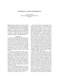
Fig. 1. Specification <strong>of</strong> the interoperability limit around amodule containing the EMI source.built. Obviously those limits are expressed in terms <strong>of</strong> absolutenumbers <strong>and</strong> depend on neither conditions <strong>of</strong> measurementsnor <strong>of</strong> numerical modeling.A typical emission problem <strong>of</strong> the module containing RF IC(EMI source) is shown on Figure 1. The module is shieldedbecause the highest magnetic field around the module shouldnot exceed the interoperability limit defined as equal to x dBmat y mm from the module. One <strong>of</strong> simulation targets is optimization<strong>of</strong> the shield design. Rigorous consideration requiresfield—circuit co-simulations using SPICE-like model <strong>of</strong> components.With fast progress in development <strong>of</strong> commercialcodes, such simulation workflows may become routine proceduresin the near future, but today they are still considered asadvanced “state <strong>of</strong> the art”. One <strong>of</strong> the reasons is that models <strong>of</strong>active components are frequently unavailable, which makes circuitpart <strong>of</strong> the workflow meaningless. In those cases sourceparameters are defined using reference data known a priori (<strong>for</strong>example, 2 mW <strong>and</strong> 50 Ohm) <strong>and</strong> simulations are per<strong>for</strong>medusing code <strong>for</strong> three-dimensional electromagnetic field computationsonly. This approach cannot take into consideration realelectromagnetic behavior <strong>of</strong> the source (IC) <strong>and</strong>, there<strong>for</strong>e, cannotprovide accurate computation <strong>of</strong> the magnitude <strong>of</strong> the field.Of course, if the excitation in the numerical model is assignedcorrectly (<strong>for</strong> example, to the PCB net carrying the highestcurrent), numerical results will indicate accurately enough theareas <strong>of</strong> highest <strong>and</strong> lowest concentration <strong>of</strong> the electromagneticfield. But it does not answer the following question we frequentlyget from EMC designers: “How high are simulated high fields<strong>and</strong> how low are low fields?” In other words, inaccurate setup <strong>of</strong>parameters <strong>of</strong> the EM source in numerical model does not allowcomparing computed fields with interoperability limits.When detailed specifications <strong>and</strong> models needed <strong>for</strong> circuitfieldco-simulations are not available, actual characteristics <strong>of</strong>the EM source may be approximated with the use <strong>of</strong> measurednear field distribution over IC: parameters <strong>of</strong> the source in thenumerical model are tuned (calibrated) in order to reach agreementbetween measured <strong>and</strong> computed fields. This task is anexample <strong>of</strong> inverse problems that are widely known in nondestructivetesting, geophysics, medical imaging (such as computedaxial tomography), remote sensing, etc. There<strong>for</strong>e, near fieldmeasurements can be applied at two stages <strong>of</strong> EMC: <strong>for</strong>improvement <strong>of</strong> the numerical model <strong>and</strong> final verification <strong>of</strong>compliance with interoperability limits. At the first stage theelectromagnetic field is measured over the IC (if possible)whereas at the second stage measurements should be done overwhole module. In both cases we want to obtain absolute values<strong>of</strong> the field magnitudes that are related with output data <strong>of</strong>measurements via correction or calibration factor [2]. The latterdepends on the measurement setup (properties <strong>of</strong> a probe, preamplifier,cables etc). In spite <strong>of</strong> the growing popularity <strong>of</strong> nearfield measurements using EMC scanners, we have not found inthe literature any general procedure to convert output voltage <strong>of</strong>the magnetic probe into absolute values <strong>of</strong> the magnetic field.Without knowledge <strong>of</strong> the calibration factor, we have to dealwith only relative values that cannot be compared with interoperabilitylimits.In this paper practical procedures to measure <strong>and</strong> simulateabsolute values <strong>of</strong> the electromagnetic field around a module areconsidered. The methodology <strong>for</strong> conversion <strong>of</strong> near fieldmeasured data into absolute values <strong>of</strong> the magnetic fields independent<strong>of</strong> the measurement conditions is given in Section 2.We obtain the calibration factor using a reference PCB thatshould be simple enough to admit accurate analytical or numericalsolution <strong>for</strong> the electromagnetic field distribution. Nearfield measurements <strong>for</strong> the reference PCB should be per<strong>for</strong>medwith the same setup as the normal IC emission measurement.Section 3 describes practical application <strong>of</strong> this methodology tonear-field measurements over a real VCO block. Section 4contains methodology how to approximate (“tune”) EM sourcesin numerical models using measured data. Simulations to verifycompliance <strong>of</strong> the module with interoperability limits areconsidered in Section 5.2. CONVERSION OF MEASURED NEAR-FIELD VALUES: PRACTICAL PROCEDURENear-field measurements are increasingly being used toprovide in<strong>for</strong>mation regarding the electric <strong>and</strong> magneticfields in the vicinity <strong>of</strong> IC cips printed circuit boards[3]–[5]. One <strong>of</strong> the reasons is that measurement <strong>of</strong> onlyinput <strong>and</strong> output signals using a network analyzer is notsufficient to analyze the per<strong>for</strong>mance <strong>and</strong> errors because, inmany cases, the in<strong>for</strong>mation obtained is not sufficient tolocalize the cause <strong>of</strong> errors.One <strong>of</strong> the popular methods to measure emissions radiatedfrom a PCB is the magnetic probe method. In this method wemeasure the output voltage (V px , V py <strong>and</strong> V pz <strong>for</strong> x-, y- <strong>and</strong> z-orientations <strong>of</strong> the probe, respectively) <strong>of</strong> the magnetic probe.The magnetic field components H x , H y , <strong>and</strong> H z are related withV px , V py <strong>and</strong> V pz , respectively, via correction or calibration factorC f as follows [2]:orH x = V px · C f ; H y = V py · C f ; H z = V pz · C f (1)H x dB = V px dB + C f dB ; H y dB = V py dB + C f dB ;H z dB = V pz dB + C f dB (2)Here V p dB is V p value in dB V <strong>and</strong> C f dB is C f value in dB S/m.There<strong>for</strong>e, the calibration factor must be known to convertthe output voltage to the magnetic field using (1)–(2). If thecalibration factor is unknown, we can obtain only relative(normalized) values <strong>of</strong> the magnetic field. According to ourexperience, application <strong>of</strong> analytical <strong>for</strong>mulae <strong>and</strong>/or calibrationcharacteristics <strong>of</strong> commercial probes are not reliable so we hadto choose another approach, namely: the calibration factor can©2009 IEEE55
e obtained using a reference (test) PCB that should be simpleenough to admit accurate analytical or numerical solution <strong>for</strong> themagnetic field distribution. Near field measurements <strong>and</strong> simulations<strong>for</strong> the reference PCB should be per<strong>for</strong>med with the same setupas the normal IC emission measurement. In this case the calibrationfactor will be the same <strong>for</strong> IC <strong>and</strong> reference PCB measurementsso that the calibration procedure will include the following steps:1. Near-field measurements over target IC to obtain Vpx ICdB ,Vpy ICICdB <strong>and</strong> Vpz dB2. Near-field measurements over reference PCB to obtainV refpx dB , V refrefpy dB <strong>and</strong> Vpz dB .3. Numerical modeling <strong>of</strong> reference PCB to obtain Hx ref ,Hyref <strong>and</strong> Hz ref .4. Calculation <strong>of</strong> the calibration factor C f dB using one <strong>of</strong>the following <strong>for</strong>mulae:Fig. 2. VCO block.C fC fdB = H refx dB − V refpx dBor C f dB = H refy dB − V refpy dBordB = H refz dB − V refpz dB(3)5. Conversion to the magnetic field values H IC<strong>and</strong> Hz ICdB using (2).x dB , HIC y dBIn the next section the procedure described is illustrated.3. EXAMPLE: MAGNETIC FIELD OVERA VCO BLOCK3.1 Near-Field <strong>Measurements</strong> Over VCOVoltage-controlled oscillator is well-known in EMC design asa source <strong>of</strong> radiation emission that usually needs to be reducedby shielding. Our first aim was measurement <strong>of</strong> the magneticfield over the VCO block shown in Figure 2 at fundamentalfrequency 3.975 GHz <strong>and</strong> detection <strong>of</strong> highest values <strong>of</strong> emission(maximum amplitudes <strong>of</strong> the magnetic field components).<strong>Measurements</strong> have been per<strong>for</strong>med in XY-plane (parallel tothe PCB) <strong>for</strong> opened VCO shield using commercial EMC scannerwith spectrum analyzer <strong>and</strong> magnetic probes with <strong>and</strong>without preamplifier. Figure 3 presents distributions <strong>of</strong>components <strong>of</strong> the magnetic field measured at 3.2 mm fromthe PCB (1 mm from top <strong>of</strong> the shield; height <strong>of</strong> the shield is2.2 mm). Maximum amplitudes <strong>of</strong> measured magnetic field atthat plane are collected in Table 1.Note thatFig. 3. X-, Y- <strong>and</strong> Z- components <strong>of</strong> the magnetic fieldmeasured over VCO block.(Vpx VCOdBm )max = max ( Vpx VCOdBm (x, y)) ; z coordinate is fixed <strong>and</strong>equal to 3.2 mm <strong>for</strong> data in Table 1.3.2 Near-Field <strong>Measurements</strong> OverReference PCBAs the reference PCB we have used a simple 50 Ohmmicrostrip line shown in Figure 4. The microstrip line wasconnected to the source <strong>of</strong> the same power level as VCO RFoutput. Figure 5 shows both the VCO board <strong>and</strong> the referenceH max ̸=√ (Hmaxx) 2+(Hmaxy) 2+(Hmaxzbecause components have their maximum at different positions soHxmaxHymaxHzmax= max ( H x (x, y) ) = Hx max (x 1 , y 1 )= max ( H y (x, y) ) = Hy max (x 2 , y 2 )= max ( H z (x, y) ) = H maxz (x 3 , y 3 )) 2Here <strong>and</strong> below Vpx VCOdBm denotes an amplitude <strong>of</strong> the probe outputvoltage, measured at point (x,y,z) above VCO, by the probeplaced in x-orientation. Maximum amplitude was detected as aresult <strong>of</strong> scanning over PCB in x- <strong>and</strong> y-directions soFig. 4. Reference PCB (50 Ohm microstrip line).56 ©2009 IEEE
TABLE 1. MAXIMUM AMPLITUDES OF THE COMPONENTS OF MEASURED MAGNETIC FIELD OVER VCO (HEIGHT IS3.2 MM FROM THE PCB, FREQUENCY IS 3.975 GHZ).( ) max, ( ) max, (maxV VCOpx dBm dBm V VCOpy dBm dBm V VCOpz dBm), dBmWithout pre-amplifier −63 −63 −61With pre-amplifier −29 −30 −27Fig. 5. VCO board (left) <strong>and</strong> reference PCB (right).Fig. 6. X-, Y- <strong>and</strong> Z- components <strong>of</strong> the magnetic fieldmeasured over reference PCB.PCB. Figure 6 shows the distribution <strong>of</strong> components <strong>of</strong> themagnetic field at 3.2 mm from the PCB at 3.975 GHz. Maximumamplitudes <strong>of</strong> components are shown in Table 2. <strong>Measurements</strong><strong>of</strong> the reference PCB have been per<strong>for</strong>med with thesame levels <strong>of</strong> pre-amplifier as in the case <strong>of</strong> VCO.3.3 Numerical Modeling Over Reference PCBFrom basic <strong>for</strong>mula (1) it follows that the output <strong>of</strong> the near-fieldprobe is directly proportional to the field intensity at the locationFig. 7. X-, Y- <strong>and</strong> Z- components <strong>of</strong> the magnetic fieldcomputed over reference PCB.<strong>of</strong> the probe. This does not allow <strong>for</strong> the fact that the presence <strong>of</strong>the probe itself may introduce some perturbation in the field componentbeing measured. There<strong>for</strong>e rigorous consideration requiresinclusion <strong>of</strong> the probe in the computational model together withthe reference PCB. Since perturbation caused by the probe is usuallyeffect <strong>of</strong> high order <strong>of</strong> magnitude, taking it into account ispossible only using an accurate <strong>and</strong> detailed model <strong>of</strong> the probe asit was done in [6] <strong>for</strong> h<strong>and</strong>made probes. In our measurement setupwe have used commercial near field probes that made modelingdifficult due to lack <strong>of</strong> in<strong>for</strong>mation about probe’s internal structure.On the other h<strong>and</strong>, our probes are smaller than those havebeen used in [6] so we can expect low disturbance within 5% [7].Thus we decided to restrict ourselves by major effects in simulation<strong>of</strong> the near-field distribution above the reference PCB <strong>and</strong> donot include the probe in the computational model. It imposeslimitations on the applicability <strong>of</strong> the technique, but their investigationrequires special consideration that is outside the content<strong>of</strong> this paper. According to our knowledge, similar assumptionshave been made in papers [8]–[10] where numerical modeling <strong>of</strong>the near field measurement setup was also considered.The electromagnetic behavior <strong>of</strong> the microstrip line wassimulated using different commercial codes <strong>for</strong> 3-D EM fieldcomputations <strong>and</strong> good agreement between numerical resultshas been observed. Figure 6 shows computed components <strong>of</strong> themagnetic field at shown in Figure 7 <strong>and</strong> their maximum amplitudescan be found in Table 3.TABLE 2. MAXIMUM AMPLITUDES OF THE COMPONENTS OF MEASURED MAGNETIC FIELD OVER REFERENCE PCB(HEIGHT IS 3.2 MM FROM THE PCB, FREQUENCY IS 3.975 GHZ).( ) max, ( ) max, (max,V refpx dBm dBm V refpy dBm dBm V refpz dBm)dBmWithout pre-amplifier −81 −69 −72With pre-amplifier −48 −37 −41©2009 IEEE57
TABLE 3. MAXIMUM AMPLITUDES OF COMPUTEDMAGNETIC FIELD COMPONENTS OVER REFERENCEPCB (HEIGHT IS 3.2 MM FROM THE PCB, FREQUENCYIS 3.975 GHZ).(Hrefx) max,A/m(Hrefy) max,A/m(Hrefz0.010 0.034 0.026) max,A/m3.4 Calculation <strong>of</strong> the Calibration FactorFormula (3) requires results <strong>of</strong> measurement <strong>and</strong> computation<strong>of</strong> only one component <strong>of</strong> the magnetic field to obtain thecalibration factor. In our case measurements <strong>of</strong> all componentshave been done using the same setup so the calibration factorshould not depend on selection <strong>of</strong> the component. For verificationwe have per<strong>for</strong>med calculations using max amplitudes <strong>of</strong>Hx, Hy, <strong>and</strong> Hz separately <strong>and</strong> results are in good agreement(+/−2 dB). As it follows from data in Table 4, the calibrationfactor in series 1 <strong>and</strong> 2 (without <strong>and</strong> with pre-amplifier) isequal to 53 <strong>and</strong> 19, respectively. <strong>Measurements</strong> were done <strong>for</strong>various positions <strong>of</strong> the probe in x-, <strong>and</strong> y- directions. It wasobserved that the calibration factor does not depend on theprobe position.<strong>Measurements</strong>, simulations <strong>and</strong> calculations <strong>of</strong> calibrationfactors have been repeated <strong>for</strong> other distances between the probe<strong>and</strong> PCB, <strong>and</strong> results are shown in Table 5. Note that thecalibration coefficients relating x-, y-, <strong>and</strong> z-components <strong>of</strong> themagnetic field to the probe voltage have almost equal values atshort distances between the probe <strong>and</strong> PCB since the electromagneticfield near a large current would be dominated by themagnetic field. However, difference between the calibrationfactors <strong>for</strong> components is growing with increase <strong>of</strong> the distancebecause the probe output might also be influenced by theelectric field.TABLE 4. CALCULATION OF THE CALIBRATION FACTOR FOR MEASUREMENTS WITHOUT AND WITH PREAMPLIFIER(SERIES 1 AND 2, RESPECTIVELY), HEIGHT IS 3.2 MM FROM THE PCB, AND FREQUENCY IS 3.975 GHZ.Measured output voltage (reference PCB) Computed magnetic field (reference PCB) Calibration factorsH-field comp.(V refpx,py,pz dBm) max (V refpx,py,pz dBV) max (H )ref max(x,y,zH refx,y,z dB) maxC f dB = H refx- −81 (series 1) −94 (series 1) 0.01 −40 54 (series 1)−48 (series 2) −61 (series 2) 21 (series 2)y- −69 (series 1) −82 (series 1) 0.034 −29 53 (series 1)−37 (series 2) −50 (series 2) 20 (series 2)z- −72 (series 1) −85 (series 1) 0.026 −32 53 (series 1)−41 (series 2) −54 (series 2) 18 (series 2)dB − Vref p dBTABLE 5. CALCULATION OF THE CALIBRATION FACTOR FOR MEASUREMENTS WITH PREAMPLIFIER FOR VARIOUSDISTANCES FROM THE PCB (FREQUENCY IS 3.975 GHZ).Measured output voltage (reference PCB) Computed magnetic field (reference PCB) Calibration factorsDistance, mmH-field comp(V refpx,py,pz dBm) max (V refpx,py,pz dBV) max (H )ref max(maxx,y,zH refx,y,z dB)C f dB5.2 x- −54 −67 0.0036 −49 18y- −44 −57 0.011 −39 18z- −49 −62 0.0087 −41 2110 x- −61 −74 0.001 −60 14y- −56 −69 0.0019 −54 15z- −59 −72 0.0019 −54 18TABLE 6. CONVERSION OF THE MEASURED OUTPUT VOLTAGE TO THE MAGNETIC FIELD OVER VCO.H field comp.(V VCOpx,py,pz dBmMeasured output voltage (VCO)) max (dBmV VCOpx,py,pz dBV) maxdB V HVCOdBMagnetic field (VCO)(= C f dB + V VCOp dBdB A/m)HVCO maxx,y,z A/mx- −63 (series 1) −76 (series 1) −23 (series 1) 0.071 (series 1)−29 (series 2) −42 (series 2) −23 (series 2) 0.071 (series 2)y- −63 (series 1) −76 (series 1) −23 (series 1) 0.071 (series 1)−30 (series 2) −43 (series 2) −24 (series 2) 0.063 (series 2)z- −61 (series 1) −74 (series 1) −21 (series 1) 0.082 (series 1)−27 (series 2) −40 (series 2) −21 (series 2) 0.082 (series 2)58 ©2009 IEEE
TABLE 7. MAGNETIC FIELD OVER VCO (3.2 MM FROM PCB, 3.975 GHZ): MEASURED, COMPUTED WITH DEFAULTPARAMETERS OF THE PORT AND COMPUTED WITH TUNED PARAMETERS OF THE PORT.( )HVCO max, ( )x A/m HVCO max, ( )y A/m HVCO max,z A/mComputed with default parameters 0.68 0.47 0.75(1 W, 50 Ohm)Computed with “tuned” parameters 0.074 0.052 0.082(0.012 W, 50 Ohm)Measured 0.071 0.063 0.0823.5 Representation <strong>of</strong> Measured MagneticField in A/mConversion <strong>of</strong> maximum amplitudes <strong>of</strong> the componentsfrom dBm to A/m was per<strong>for</strong>med using (2) <strong>and</strong> results areshown in Table 6. It is easily seen that data measured without<strong>and</strong> with pre-amplifier (series 1 <strong>and</strong> 2, respectively) ledto very close values <strong>of</strong> the magnetic field (disagreement is1dB). So results do not depend on the measurement setup<strong>and</strong> do indeed give absolute values <strong>of</strong> the magnetic fieldcomponents.4. “TUNING” PARAMETERS OF THE EMSOURCES IN NUMERICAL MODELSUSING MEASURED DATAConsider now the computation <strong>of</strong> the magnetic field aroundIC when no data <strong>for</strong> rigorous modeling <strong>of</strong> the source behavioris available. One <strong>of</strong> the most popular approaches to setupexcitation in commercial tools <strong>for</strong> 3D EM field computationis definition <strong>of</strong> characteristics <strong>of</strong> current flowing through aconductor using so-called discrete or lumped port (physicalrepresentation similar to Hertzian dipole). Usually power (P)<strong>and</strong> resistance (R) <strong>of</strong> the port should be defined, default valuesare 1 W <strong>and</strong> 50 Ohm, respectively, but how can we knowactual values in a given case? The answer becomes clear if wehave already measured the magnetic field over the PCB:parameters <strong>of</strong> the port can be approximated by solvinginverse problem. In many practical cases the problem is linear<strong>and</strong> advanced commercial codes allow P <strong>and</strong> R to vary atthe post-processing stage so the procedure consists <strong>of</strong> the followingsteps:1. Model real IC by set <strong>of</strong> ports assigned to the nets carryinghighest current. This requires a priori knowledge aboutgeneral EM behavior <strong>of</strong> the module/device.2. Run simulations with default values <strong>of</strong> parameters <strong>of</strong> theports.3. Compare computed <strong>and</strong> measured distributions <strong>of</strong> theEM field at specified height over the PCB <strong>and</strong> “tune”parameters <strong>of</strong> the port to reach agreement betweenmeasured data <strong>and</strong> numerical results.Consider again our VCO block. From specification it isknown that the highest current is flowing in the “RF output”net. The simplest model <strong>of</strong> the VCO block consists <strong>of</strong>this net with assigned port, PCB represented as solid metalbrick <strong>and</strong> walls <strong>of</strong> the shield (Figure 8). All parts are assumedto be copper.Numerical results be<strong>for</strong>e <strong>and</strong> after tuning are showntogether with measured data in Table 7. It is easily to seeFig. 8. Simplest model <strong>of</strong> the VCO block without cover <strong>of</strong>the shield.that setting up the port power <strong>and</strong> resistance equal to 0.012W <strong>and</strong> 50 Ohm, respectively, provides good agreementbetween measured <strong>and</strong> computed components <strong>of</strong> the magneticfield at 3.2 mm from the PCB. Those parameters canthen be used in 3D EM simulations <strong>of</strong> all problems wherethis VCO is the excitation source.Although the port in our numerical model is assigned to oneparticular net (RF output), parameters <strong>of</strong> the port are tunedusing the highest values <strong>of</strong> emission from whole VCO block.There<strong>for</strong>e, VCO output power, related with current flowing inthe RF output net, should not be mixed with tuned power <strong>of</strong>the port in the numerical model. As it is seen on Figure 3, maximumin the EM field distribution takes place not over the RFoutput net so VCO output power, equal to 2 mW according tospecification, is significantly less than 0.012 W.It is natural to ask the question: will the port with parameterstuned <strong>for</strong> one distance from the IC to observation pointdescribe correctly EM field at other distances? From theoreticalpoint <strong>of</strong> view—yes, as long as this distance remains much largerthan characteristic size <strong>of</strong> the IC. In other words, until theHertzian dipole approximation can be applied. There<strong>for</strong>e, it isenough to tune parameters <strong>of</strong> the port just once <strong>for</strong> a certainfrequency <strong>and</strong> then apply them <strong>for</strong> the EM field computationsat wide range <strong>of</strong> distances.Figures 9(a)–9(c) show measured <strong>and</strong> computed distributions<strong>of</strong> maximum amplitudes <strong>of</strong> the components <strong>of</strong> the magneticfield with increase <strong>of</strong> distance from VCO. Radiation inVCO takes place not only from RF output net as it is assumedin our simplest numerical model. This is the most probablereason <strong>of</strong> some disagreements between measured <strong>and</strong> computedcurves in Figures 9(b)–9(c). Another reason may berelated with the fact that converted measured data are lessaccurate at “far” distances from the board as it was discussedin Section 3.4.©2009 IEEE59
Fig. 10. VCO shield.a)Fig. 11. Magnetic field (magnitude) at 5 mm above theVCO shield.b)c)Fig. 9. (a) Maximum amplitude <strong>of</strong> x-component <strong>of</strong> themagnetic field as a function <strong>of</strong> the distance from PCB. (b)Maximum amplitude <strong>of</strong> y-component <strong>of</strong> the magnetic fieldas a function <strong>of</strong> the distance from PCB. (c) Maximumamplitude <strong>of</strong> z-component <strong>of</strong> the magnetic field as a function<strong>of</strong> the distance from PCB.5. VERIFICATION OF COMPLIANCEWITH INTEROPERABILITY LIMITSBY SIMULATIONSIn practice IC components are supplied by third-party vendors <strong>and</strong>frequently it is much easier to get results <strong>of</strong> near fieldmeasurements than detailed specifications <strong>and</strong> models needed <strong>for</strong>circuit-field co-simulations. In such cases measured data can beused <strong>for</strong> numerical modeling <strong>of</strong> EM behavior <strong>of</strong> the module/device<strong>and</strong> verification <strong>of</strong> compliance with interoperability limits.Consider the following “toy” example to illustrate the methodology.Suppose the cover <strong>of</strong> the VCO shield has a slot as shown inFigure 10. Let our target be optimization <strong>of</strong> the length L <strong>of</strong> the slot:it should be as long as possible, but magnitude <strong>of</strong> the magnetic fieldat 5 mm from the top <strong>of</strong> the VCO should not exceed −90 dBm.Note that this task cannot be achieved by calculation <strong>of</strong> shieldingeffectiveness without taking into account EM source characteristics.Three-dimensional EM field computations have been per<strong>for</strong>medusing the port parameters tuned in the previous section. Examples<strong>of</strong> magnetic field distributions <strong>for</strong> slots <strong>of</strong> various lengths are shownin Figure 11. It is easily seen that increase <strong>of</strong> length from 0.5 mmto 2 mm causes sharp growth <strong>of</strong> the electromagnetic field emissionfrom the shield. Figure 12 demonstrates maximum magnitude <strong>of</strong>the magnetic field at 5 mm over the shield as a function <strong>of</strong> length<strong>of</strong> the slot. From this figure is follows that interoperability limitwill be exceeded <strong>for</strong> slot longer than 0.9 mm.Procedures <strong>of</strong> tuning parameters <strong>of</strong> the port, verification <strong>of</strong>compliance with interoperability limit <strong>and</strong> optimization <strong>of</strong>design are summarized <strong>and</strong> shown as the workflow in Figure 13.CONCLUSIONSIn the present paper a set <strong>of</strong> two principal methodologies havebeen described:60 ©2009 IEEE
Fig. 12. Maximum magnetic field (magnitude) at 5 mmabove VCO shield as function <strong>of</strong> length <strong>of</strong> the slot.1. Methodology to convert EMC scanner output data(voltage measured in dBm) into absolute values <strong>of</strong>magnetic fields independent <strong>of</strong> the measurementconditions <strong>and</strong> expressed in A/m. This is done usingreference PCB that is simple enough to enable accuratenumerical modeling. Results <strong>of</strong> measurement <strong>and</strong>modeling <strong>of</strong> reference PCB are used to obtain thecalibration factor that is then applied to IC measureddata.2. Methodology to calibrate (tune) EM sources in numericalmodels using measured data by solving the inverse problem.It enables the simulation <strong>of</strong> absolute (as opposed tonormalized) values <strong>of</strong> EM field emission without detailedknowledge <strong>of</strong> the source properties.Validation <strong>of</strong> the methodologies is done by:• Calculation <strong>of</strong> the calibration factor <strong>for</strong> different components<strong>of</strong> H-field at various positions <strong>of</strong> the probe (to make sure thecalibration factor does not depend on the probe position).• Numerical modeling <strong>of</strong> reference PCB using variouscommercial simulation tools.• Repeating measurements with <strong>and</strong> without pre-amplifier(different calibration factors), leading to the same absolutevalues <strong>of</strong> the magnetic fieldsApplication <strong>of</strong> both methodologies to a test problem <strong>of</strong>emission from a VCO IC is demonstrated. Numerical modeling<strong>of</strong> the electromagnetic behavior <strong>of</strong> reference PCB (to obtaincalibration coefficients) has been per<strong>for</strong>med neglecting theprobe interaction with the field measured. This assumption canbe avoided by inclusion <strong>of</strong> the probe into computational model<strong>of</strong> the measurement setup <strong>and</strong> it would be the next step in thiswork. Numerical results being compared with interoperabilitylimit enable to make verdict “Ok/Not Ok” <strong>for</strong> various designoptions <strong>of</strong> the VCO shield.REFERENCES[1] A. Drozd, “Progress on the development <strong>of</strong> st<strong>and</strong>ards <strong>and</strong> recommended practices<strong>for</strong> CEM computer modeling <strong>and</strong> code validation,” Proceedings <strong>of</strong> IEEEInternational Symposium on Electromagnetic Compatibility, pp. 313–316, 2003.[2] “Measurement <strong>of</strong> conducted emissions—magnetic probe method,” InternationalSt<strong>and</strong>ard IEC 61967-6, Part 6, 2002.[3] Y. Gao, A. Lauer, Q. Ren, <strong>and</strong> I. Wolff, “Calibration <strong>of</strong> electric coaxial nearfieldprobes <strong>and</strong> applications,” IEEE Transactions Microwave Theory <strong>Techniques</strong>,vol. 46, no. 11, pp. 1694–1703.Fig. 13. Proposed workflow to verify compliance withinteroperability limits by numerical modeling.[4] K. Slattery, J. Neal, <strong>and</strong> W. Cui, “Near-field measurements <strong>of</strong> VLSI devices,”IEEE Transactions Electromagnetic Compatibility, vol. 41, pp. 374–384, 1999.[5] H. Funato <strong>and</strong> T. Suga, “Magnetic near-field probe <strong>for</strong> CHz b<strong>and</strong> <strong>and</strong> spatialresolution improvement technique,” Proceedings <strong>of</strong> 17th InternationalZurich Symposium on Electromagnetic Compatibility, pp. 284–287, 2006.[6] J. Shi, M. Cracraft, K. Slattery, M. Yamaguchi, <strong>and</strong> R. DuBr<strong>of</strong>f “Calibration<strong>and</strong> compensation <strong>of</strong> near-field measurements,” IEEE TransactionsElectromagnetic Compatibility, vol. 47, pp. 642–650, 2005.[7] W. Joseph <strong>and</strong> L. Martens, “The influence <strong>of</strong> the measurement probe on theevaluation <strong>of</strong> electromagnetic fields,” IEEE Transactions Electromagnetic Compatibility,vol. 43, no. 2, pp. 339–649, 2003.[8] C. Chen, N. Nagaoka, T. Anada, K. Li, Z. Ma, <strong>and</strong> C. Christopoulos, “Nearelectric field in microstrip/coplanar circuits <strong>and</strong> antennas —simulation <strong>and</strong>measurement,” Proceedings IEEE International Symposium on ElectromagneticCompatibility, pp. 108–113, 2006.[9] K. Srinivasan, H. Sasaki, M. Swaminathan, <strong>and</strong> R. Tummala, “Calibration<strong>of</strong> near field measurements using microstrip line <strong>for</strong> noise prediction,” Proceedings<strong>of</strong> Electronic Components <strong>and</strong> Technology Conf., pp. 1432–1436, 2004.[10] M. Takahashi, H. Ota, K.I. Arai, <strong>and</strong> R. Sato, “A study on magneticnear-field measurements above a patch antenna using an optical waveguideprobe with loop element,” IEICE Transactions on Communications,vol., E88-B, no. 8, pp. 3140–3145, 2005.BIOGRAPHIESSergey Yuferev was born in St. Petersburg, Russia,in 1964. He has received the M.Sc. degree in computationalfluid mechanics from the St. Petersburg TechnicalUniversity in 1987 <strong>and</strong> the Ph.D. degree from theA.F.I<strong>of</strong>fe Institute in 1992. From 1987 to 1998, hewas with the Dense Plasma Dynamics Laboratory <strong>of</strong> theA.F.I<strong>of</strong>fe Institute. From 1999 to 2000, he was a VisitingAssociate Pr<strong>of</strong>essor <strong>of</strong> Electrical Engineering at The University <strong>of</strong>Ohio, in Akron. Since 2000, he has been with Nokia Corp., Finl<strong>and</strong>. Hiscurrent research interests are in the areas <strong>of</strong> numerical modeling <strong>of</strong> electromagneticfields, EMC/EMI problems <strong>of</strong> mobile phones, perturbation methodsin electromagnetics, <strong>and</strong> surface impedance concepts.Esa Saunamäki was born in Seinäjoki, Finl<strong>and</strong>in 1971. He received the electronics technician degreein 1991 from the Technical College <strong>of</strong> Kurikka,Finl<strong>and</strong>. After graduation, he worked <strong>for</strong> severalyears in the electronic care <strong>and</strong> maintenance areas.He joined Nokia Mobile Phones in 1998. He wasquickly promoted to work on EMC design challengesin Nokia. Currently he is working with mobile phone EMC issues asan EMC Senior Design Engineer.©2009 IEEE61