HMC434(E) - Hittite Microwave
HMC434(E) - Hittite Microwave
HMC434(E) - Hittite Microwave

You also want an ePaper? Increase the reach of your titles
YUMPU automatically turns print PDFs into web optimized ePapers that Google loves.
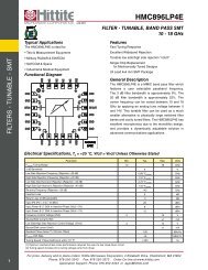
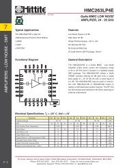
v04.0410<strong>HMC434</strong> / 434ESMT GaAs HBT MMICDIVIDE-BY-8, DC - 8 GHz4FREQUENCY DIVIDERS & DETECTORS - SMTTypical ApplicationsPrescaler for DC to C Band PLL Applications:• UNII, Pt. - Pt. & VSAT Radios• 802.11a & HiperLAN WLAN• Fiber Optic• Cellular / 3G InfrastructureFunctional DiagramFeaturesUltra Low SSB Phase Noise: -150 dBc/HzSingle-Ended I/O’sOutput Power: -2 dBmSingle DC Supply: +3V @ 62 mA9 mm 2 Ultra Small Package: SOT26General DescriptionElectrical Specifications, T A= +25° C, 50 Ohm System, Vcc= +3VThe <strong>HMC434</strong>(E) is a low noise Divide-by-8 StaticDivider utilizing InGaP GaAs HBT technology inultra small surface mount SOT26 plastic packages.This device operates from DC (with a square waveinput) to 8 GHz input frequency with a single +3VDC supply. Single-ended inputs and outputs reducecomponent count and cost. The low additive SSBphase noise of -150 dBc/Hz at 100 kHz offset helpsthe user maintain good system noise performance.Parameter Conditions Min. Typ. Max. UnitsMaximum Input Frequency 8 8.5 GHzMinimum Input Frequency Sine Wave Input. [1] 0.2 GHzInput Power RangeFin= 1 to 3 GHzFin= 3 to 7 GHzFin= 7 to 8 GhzOutput Power Fin= 1 to 8 GHz -5.0 -2.0 dBmReverse Leakage RF Output Terminated, Fin= 4 GHz, Pin= 0 dBm -20 dBmSSB Phase Noise (100 kHz offset) Pin= 0 dBm, Fin= 4 GHz -150 dBc/HzOutput Transition Time Pin= 0 dBm, Fout= 882 MHz 140 psSupply Current (Icc) Vcc= +3.0V 62 83 mA1. Divider will operate down to DC for square-wave input signal.-10-30+12+12+10dBmdBmdBm4 - 78For price, delivery and to place orders: <strong>Hittite</strong> <strong>Microwave</strong> Corporation, 20 Alpha Road, Chelmsford, MA 01824Phone: 978-250-3343 Fax: 978-250-3373 Order On-line at www.hittite.comApplication Support: Phone: 978-250-3343 or apps@hittite.com
v04.0410<strong>HMC434</strong> / 434ESMT GaAs HBT MMICDIVIDE-BY-8, DC - 8 GHzInput Sensitivity Window, T= 25 °C2015Input Sensitivity Window vs. Temperature20154INPUT POWER (dBm)1050-5-10-15RecommendedOperating Window-200 1 2 3 4 5 6 7 8 9 10INPUT FREQUENCY (GHz)Output Power vs. TemperatureOUTPUT POWER (dBm)Output HarmonicContent, Pin= 0 dBm, T= 25 °COUTPUT LEVEL (dBm)0-1-2-3-4-50 1 2 3 4 5 6 7 8 9 100-10-20-30-40+25 C-40 C+75 CINPUT FREQUENCY (GHz)Pfeedthru2nd Harmonic3rd HarmonicINPUT POWER (dBm)SSB Phase NoisePerformance, Pin= 0 dBm, T= 25 °CSSB PHASE NOISE (dBc/Hz)0-20-40-60-80-100-120-140-16010 2 10 3 10 4 10 5 10 6 10 7OFFSET FREQUENCY (Hz)Reverse Leakage, Pin= 0 dBm, T= 25 °CPOWER LEVEL (dBm)1050-5-10-15-200 1 2 3 4 5 6 7 8 9 100-10-20-30-40-50Min Pin +25 CMax Pin +25 CMin Pin -40 CMax Pin -40 CMin Pin +85 CMax Pin +85 CINPUT FREQUENCY (GHz)FREQUENCY DIVIDERS & DETECTORS - SMT-500 1 2 3 4 5 6 7 8 9 10INPUT FREQUENCY (GHz)-600 2 4 6 8 10INPUT FREQUENCY (GHz)For price, delivery and to place orders: <strong>Hittite</strong> <strong>Microwave</strong> Corporation, 20 Alpha Road, Chelmsford, MA 01824Phone: 978-250-3343 Fax: 978-250-3373 Order On-line at www.hittite.comApplication Support: Phone: 978-250-3343 or apps@hittite.com4 - 79
v04.0410<strong>HMC434</strong> / 434ESMT GaAs HBT MMICDIVIDE-BY-8, DC - 8 GHz4Output Voltage Waveform,Pin= 0 dBm, Fout= 882 MHz, T= 25 °C300200FREQUENCY DIVIDERS & DETECTORS - SMTAMPLITUDE (mV)1000-100-200-30022.7 23.1 23.5 23.9 24.3 24.7TIME (nS)Absolute Maximum RatingsRF Input Power (Vcc = +3V)15 dBmNominal +3V Supply to GND-0.3V to +3.5VMax Peak Flow Temperature 260 °CStorage Temperature -65 to +125 °CDC blocking capacitors are required at RF input and RF output ports.Choose value for lowest frequency of operation.ELECTROSTATIC SENSITIVE DEVICEOBSERVE HANDLING PRECAUTIONSReliability InformationJunction Temperature to Maintain1 Million Hour MTTF135 °CNominal Junction Temperature(T = 85 °C)99 °CThermal Resistance(Junction to GND Paddle, 3V Supply)70 °C/WOperating Temperature -40 to +85 °CTypical Supply Current vs. VccVcc (V)Icc (mA)2.70 503.0 623.30 74Note: Divider will operate over full voltage range shown above4 - 80For price, delivery and to place orders: <strong>Hittite</strong> <strong>Microwave</strong> Corporation, 20 Alpha Road, Chelmsford, MA 01824Phone: 978-250-3343 Fax: 978-250-3373 Order On-line at www.hittite.comApplication Support: Phone: 978-250-3343 or apps@hittite.com
v04.0410<strong>HMC434</strong> / 434ESMT GaAs HBT MMICDIVIDE-BY-8, DC - 8 GHzOutline Drawing4Package InformationPin DescriptionPin Number Function Description Interface Schematic1, 4 N/CThe pins are not connected internally; however, alldata shown herein was measured with these pinsconnected to RF/DC ground externally.NOTES:1. LEADFRAME MATERIAL: COPPER ALLOY2. DIMENSIONS ARE IN INCHES [MILLIMETERS]3. LEAD SPACING TOLERANCE IS NON-CUMULATIVE.4. PAD BURR LENGTH SHALL BE 0.15mm MAXIMUM.PAD BURR HEIGHT SHALL BE 0.05mm MAXIMUM.5. PACKAGE WARP SHALL NOT EXCEED 0.05mm.6. ALL GROUND LEADS AND GROUND PADDLE MUST BESOLDERED TO PCB RF GROUND.7. REFER TO HITTITE APPLICATION NOT FOR SUGGESTEDLAND PATTERN.Part Number Package Body Material Lead Finish MSL Rating Package Marking [3][1] H434<strong>HMC434</strong> Low Stress Injection Molded Plastic Sn/Pb Solder MSL1XXXX[2] 434E<strong>HMC434</strong>E RoHS-compliant Low Stress Injection Molded Plastic 100% matte Sn MSL1XXXX[1] Max peak refl ow temperature of 235 °C[2] Max peak refl ow temperature of 260 °C[3] 4-Digit lot number XXXXFREQUENCY DIVIDERS & DETECTORS - SMT2 GND Pin must connect ro RF/DC ground.3 IN RF input must be DC blocked.For price, delivery and to place orders: <strong>Hittite</strong> <strong>Microwave</strong> Corporation, 20 Alpha Road, Chelmsford, MA 01824Phone: 978-250-3343 Fax: 978-250-3373 Order On-line at www.hittite.comApplication Support: Phone: 978-250-3343 or apps@hittite.com4 - 81
v04.0410<strong>HMC434</strong> / 434ESMT GaAs HBT MMICDIVIDE-BY-8, DC - 8 GHz4Pin Description (Continued)Pin Number Function Description Interface Schematic5 Vcc Supply voltage 3V ± 0.3V.FREQUENCY DIVIDERS & DETECTORS - SMT6 OUT Divided output must be DC blocked.Application CircuitNote: Line lengths on pins 1 & 4(N/C) are not necessary.Note:DC blocking capacitor values (C1, C2) and DC decoupling capacitorvalues (C3, C4) are chosen for lowest frequency of operation.4 - 82For price, delivery and to place orders: <strong>Hittite</strong> <strong>Microwave</strong> Corporation, 20 Alpha Road, Chelmsford, MA 01824Phone: 978-250-3343 Fax: 978-250-3373 Order On-line at www.hittite.comApplication Support: Phone: 978-250-3343 or apps@hittite.com
v04.0410<strong>HMC434</strong> / 434ESMT GaAs HBT MMICDIVIDE-BY-8, DC - 8 GHzEvaluation PCB4List of Materials for Evaluation PCB 105675 [1]ItemDescriptionJ1 - J2PCB Mount SMA RF ConnectorJ3 - J4DC PinC1 - C2100 pF Capacitor, 0402 Pkg.C31000 pF Capacitor, 0402 Pkg.C410 μF Tantalum Capacitor, 1206 Pkg.U1<strong>HMC434</strong> / <strong>HMC434</strong>E Divide-by-8PCB [2]105199 Eval Board[1] Reference this number when ordering complete evaluation PCB[2] Circuit Board Material: Rogers 4350The circuit board used in the application should useRF circuit design techniques. Signal lines shouldhave 50 Ohm impedance while the package groundleads should be connected directly to the groundplane similar to that shown. A sufficient number ofvia holes should be used to connect the top andbottom ground planes. The evaluation circuit boardshown is available from <strong>Hittite</strong> upon request.FREQUENCY DIVIDERS & DETECTORS - SMTFor price, delivery and to place orders: <strong>Hittite</strong> <strong>Microwave</strong> Corporation, 20 Alpha Road, Chelmsford, MA 01824Phone: 978-250-3343 Fax: 978-250-3373 Order On-line at www.hittite.comApplication Support: Phone: 978-250-3343 or apps@hittite.com4 - 83