HX8347-D - Mikrocontroller.net
HX8347-D - Mikrocontroller.net
HX8347-D - Mikrocontroller.net
- No tags were found...

You also want an ePaper? Increase the reach of your titles
YUMPU automatically turns print PDFs into web optimized ePapers that Google loves.
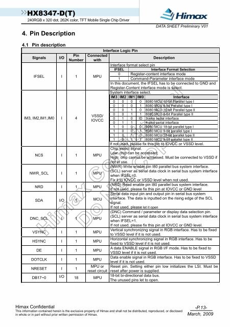
<strong>HX8347</strong>-D(T)240RGB x 320 dot, 262K color, TFT Mobile Single Chip Driver4. Pin DescriptionDATA SHEET Preliminary V014.1 Pin descriptionInterface Logic PinPin ConnectedSignals I/ODescriptionNumber withInterface format select pinIFSELInterface Format Selection0 Register-content interface modeIFSEL I 1 MPU1 Command-Parameter interface modeIn this document, the IFSEL has to be connected to GND andRegister-Content interface mode is select.System interface select.IM3 IM2 IM1 IM0Interface0 0 0 0 8080 MCU 16-bit Parallel type I0 0 0 1 8080 MCU 8-bit Parallel type I0 0 1 0 8080 MCU 16-bit Parallel type II0 0 1 1 8080 MCU 8-bit Parallel type IIVSSD/IM3, IM2,IM1,IM0 I 40 1 0 ID 3-wire serial interfaceIOVCC0 1 1 - 4-wire serial interface1 0 0 0 8080 MCU 18-bit parallel type I1 0 0 1 8080 MCU 9-bit parallel type I1 0 1 0 8080 MCU 18-bit parallel type II1 0 1 1 8080 MCU 9-bit parallel type IIIf not used, please fix this pin to IOVCC or VSSD level.Chip select signal.Low: chip can be accessed;NCS I 1 MPUHigh: chip cannot be accessed. Must be connected to VSSD ifnot in use.(NWR) Write enable pin I80 parallel bus system interface.(SCL) server as serial data clock in serial bus system interfaceNWR_SCL I 1 MPUwhen IFSEL=0.Fix it to IOVCC or VSSD level when not used.(NRD) Read enable pin I80 parallel bus system interface.NRD I 1 MPUIf not used, please fix this pin at IOVCC or GND levelSerial data input pin and output pin in serial bus systemSDA I/O 1 MCU interface. The data is inputted on the rising edge of the SCLsignal.If not used, please let it open(DNC) Command / parameter or display data selection pin.(SCL) server as serial data clock in serial bus system interfaceDNC_SCL I 1 MPUwhen IFSEL=1.If not used, please fix this pin at IOVCC or GND level.Vertical synchronizing signal in RGB interface. Has to be fixedVSYNC I 1 MPUto VSSD level if it is not used.Horizontal synchronizing signal in RGB interface. Has to beHSYNC I 1 MPUfixed to VSSD level if it is not used.A data ENABLE signal in RGB I/F mode. Has to be fixed toDE I 1 MPUVSSD level if it is not used.Data enable signal in RGB interface. Has to be fixed to VSSDDOTCLK I 1 MPUNRESET I 1MPU orreset circuitDB17~0 I/O 18 MPUlevel if it is not used.Reset pin. Setting either pin low initializes the LSI. Must bereset after power is supplied.18-bit bi-directional data bus.The unused pins let to open.Himax ConfidentialThis information contained herein is the exclusive property of Himax and shall not be distributed, reproduced, or disclosedin whole or in part without prior written permission of Himax.-P.13-March, 2009