SS8550 PNP Epitaxial Silicon Transistor
SS8550 PNP Epitaxial Silicon Transistor SS8550 PNP Epitaxial Silicon Transistor
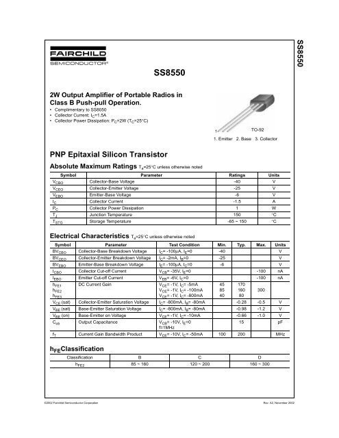
SS8550SS85502W Output Amplifier of Portable Radios inClass B Push-pull Operation.• Complimentary to SS8050• Collector Current: I C =1.5A• Collector Power Dissipation: P C =2W (T C =25°C)1TO-921. Emitter 2. Base 3. CollectorPNP Epitaxial Silicon TransistorAbsolute Maximum Ratings T a =25°C unless otherwise notedSymbol Parameter Ratings UnitsV CBO Collector-Base Voltage -40 VV CEO Collector-Emitter Voltage -25 VV EBO Emitter-Base Voltage -6 VI C Collector Current -1.5 AP C Collector Power Dissipation 1 WT J Junction Temperature 150 °CT STG Storage Temperature -65 ~ 150 °CElectrical Characteristics T a =25°C unless otherwise notedSymbol Parameter Test Condition Min. Typ. Max. UnitsBV CBO Collector-Base Breakdown Voltage I C = -100µA, I E =0 -40 VBV CEO Collector-Emitter Breakdown Voltage I C = -2mA, I B =0 -25 VBV EBO Emitter-Base Breakdown Voltage I E = -100µA, I C =0 -6 VI CBO Collector Cut-off Current V CB = -35V, I E =0 -100 nAI EBO Emitter Cut-off Current V EB = -6V, I C =0 -100 nAh FE1 DC Current Gain V CE = -1V, I C = -5mAh FE3 V CE = -1V, I C = -800mAh FE2V CE = -1V, I C = -100mAV CE (sat) Collector-Emitter Saturation Voltage I C = -800mA, I B = -80mA -0.28 -0.5 VV BE (sat) Base-Emitter Saturation Voltage I C = -800mA, I B = -80mA -0.98 -1.2 VV BE (on) Base-Emitter on Voltage V CE = -1V, I C = -10mA -0.66 -1.0 VC ob Output Capacitance V CB = -10V, I E =015 pFf=1MHzf T Current Gain Bandwidth Product V CE = -10V, I C = -50mA 100 200 MHzh FE ClassificationClassification B C Dh FE2 85 ~ 160 120 ~ 200 160 ~ 30045854017016080300©2002 Fairchild Semiconductor Corporation Rev. A2, November 2002
- Page 2 and 3: Typical CharacteristicsSS8550-0.5IB
- Page 4: TRADEMARKSThe following are registe
<strong>SS8550</strong><strong>SS8550</strong>2W Output Amplifier of Portable Radios inClass B Push-pull Operation.• Complimentary to SS8050• Collector Current: I C =1.5A• Collector Power Dissipation: P C =2W (T C =25°C)1TO-921. Emitter 2. Base 3. Collector<strong>PNP</strong> <strong>Epitaxial</strong> <strong>Silicon</strong> <strong>Transistor</strong>Absolute Maximum Ratings T a =25°C unless otherwise notedSymbol Parameter Ratings UnitsV CBO Collector-Base Voltage -40 VV CEO Collector-Emitter Voltage -25 VV EBO Emitter-Base Voltage -6 VI C Collector Current -1.5 AP C Collector Power Dissipation 1 WT J Junction Temperature 150 °CT STG Storage Temperature -65 ~ 150 °CElectrical Characteristics T a =25°C unless otherwise notedSymbol Parameter Test Condition Min. Typ. Max. UnitsBV CBO Collector-Base Breakdown Voltage I C = -100µA, I E =0 -40 VBV CEO Collector-Emitter Breakdown Voltage I C = -2mA, I B =0 -25 VBV EBO Emitter-Base Breakdown Voltage I E = -100µA, I C =0 -6 VI CBO Collector Cut-off Current V CB = -35V, I E =0 -100 nAI EBO Emitter Cut-off Current V EB = -6V, I C =0 -100 nAh FE1 DC Current Gain V CE = -1V, I C = -5mAh FE3 V CE = -1V, I C = -800mAh FE2V CE = -1V, I C = -100mAV CE (sat) Collector-Emitter Saturation Voltage I C = -800mA, I B = -80mA -0.28 -0.5 VV BE (sat) Base-Emitter Saturation Voltage I C = -800mA, I B = -80mA -0.98 -1.2 VV BE (on) Base-Emitter on Voltage V CE = -1V, I C = -10mA -0.66 -1.0 VC ob Output Capacitance V CB = -10V, I E =015 pFf=1MHzf T Current Gain Bandwidth Product V CE = -10V, I C = -50mA 100 200 MHzh FE ClassificationClassification B C Dh FE2 85 ~ 160 120 ~ 200 160 ~ 30045854017016080300©2002 Fairchild Semiconductor Corporation Rev. A2, November 2002
Typical Characteristics<strong>SS8550</strong>-0.5IB=-4.0mA1000VCE = -1VIC[mA], COLLECTOR CURRENT-0.4-0.3-0.2-0.1IB=-3.5mAIB=-3.0mAIB=-2.5mAIB=-2.0mAIB=-1.5mAIB=-1.0mAIB=-0.5mAhFE, DC CURRENT GAIN10010-0.4 -0.8 -1.2 -1.6 -2.01-0.1 -1 -10 -100 -1000VCE[V], COLLECTOR-EMITTER VOLTAGEIC[mA], COLLECTOR CURRENTFigure 1. Static CharacteristicFigure 2. DC current GainVBE(sat), VCE(sat)[V], SATURATION VOLTAGE-10000-1000-100VBE(sat)VCE(sat)IC=10IB-10-0.1 -1 -10 -100 -1000IC[mA], COLLECTOR CURRENT-100-10-1VCE = -1V-0.1-0.0 -0.2 -0.4 -0.6 -0.8 -1.0 -1.2IC[mA], COLLECTOR CURRENTVBE[V], BASE-EMITTER VOLTAGEFigure 3. Base-Emitter Saturation VoltageCollector-Emitter Saturation VoltageFigure 4. Base-Emitter On VoltageCob[pF], CAPACITANCE10010f=1MHzIE=01-1 -10 -100 -1000fT[MHz], CURRENT GAIN-BANDWIDTH PRODUCT1000100VCE=-10V10-1 -10 -100 -1000VCB[V], COLLECTOR-BASE VOLTAGEIC[mA], COLLECTOR CURRENTFigure 5. Collector Output CapacitanceFigure 6. Current Gain Bandwidth Product©2002 Fairchild Semiconductor CorporationRev. A2, November 2002
Package Dimensions<strong>SS8550</strong>TO-924.58 +0.25–0.153.86MAX0.46 ±0.101.27TYP[1.27 ±0.20]1.02 ±0.100.38 +0.10–0.051.27TYP[1.27 ±0.20]3.60 ±0.20(R2.29)(0.25) 14.47 ±0.404.58 ±0.200.38 +0.10–0.05Dimensions in Millimeters©2002 Fairchild Semiconductor Corporation Rev. A2, November 2002
TRADEMARKSThe following are registered and unregistered trademarks Fairchild Semiconductor owns or is authorized to use and is notintended to be an exhaustive list of all such trademarks.ACExActiveArrayBottomlessCoolFETCROSSVOLTDOMEEcoSPARKE 2 CMOSEnSignaFACTFACT Quiet seriesFAST ®FASTrFRFETGlobalOptoisolatorGTOHiSeCI 2 CAcross the board. Around the world.The Power FranchiseProgrammable Active DroopImpliedDisconnectISOPLANARLittleFETMicroFETMicroPakMICROWIREMSXMSXProOCXOCXProOPTOLOGIC ®OPTOPLANARPACMANPOPPower247PowerTrench ®QFETQSQT OptoelectronicsQuiet SeriesRapidConfigureRapidConnectSILENT SWITCHER ®SMART STARTSPMStealthSuperSOT-3SuperSOT-6SuperSOT-8SyncFETTinyLogicTruTranslationUHCUltraFET ®VCXDISCLAIMERFAIRCHILD SEMICONDUCTOR RESERVES THE RIGHT TO MAKE CHANGES WITHOUT FURTHER NOTICE TO ANYPRODUCTS HEREIN TO IMPROVE RELIABILITY, FUNCTION OR DESIGN. FAIRCHILD DOES NOT ASSUME ANYLIABILITY ARISING OUT OF THE APPLICATION OR USE OF ANY PRODUCT OR CIRCUIT DESCRIBED HEREIN;NEITHER DOES IT CONVEY ANY LICENSE UNDER ITS PATENT RIGHTS, NOR THE RIGHTS OF OTHERS.LIFE SUPPORT POLICYFAIRCHILD’S PRODUCTS ARE NOT AUTHORIZED FOR USE AS CRITICAL COMPONENTS IN LIFE SUPPORTDEVICES OR SYSTEMS WITHOUT THE EXPRESS WRITTEN APPROVAL OF FAIRCHILD SEMICONDUCTORCORPORATION.As used herein:1. Life support devices or systems are devices or systemswhich, (a) are intended for surgical implant into the body,or (b) support or sustain life, or (c) whose failure to performwhen properly used in accordance with instructions for useprovided in the labeling, can be reasonably expected toresult in significant injury to the user.PRODUCT STATUS DEFINITIONSDefinition of Terms2. A critical component is any component of a life supportdevice or system whose failure to perform can bereasonably expected to cause the failure of the life supportdevice or system, or to affect its safety or effectiveness.Datasheet Identification Product Status DefinitionAdvance InformationFormative or InDesignThis datasheet contains the design specifications forproduct development. Specifications may change inany manner without notice.Preliminary First Production This datasheet contains preliminary data, andsupplementary data will be published at a later date.Fairchild Semiconductor reserves the right to makechanges at any time without notice in order to improvedesign.No Identification Needed Full Production This datasheet contains final specifications. FairchildSemiconductor reserves the right to make changes atany time without notice in order to improve design.Obsolete Not In Production This datasheet contains specifications on a productthat has been discontinued by Fairchild semiconductor.The datasheet is printed for reference information only.©2002 Fairchild Semiconductor Corporation Rev. I1


