Virtex-5 FPGA Board XCM-109 Series User's Manual
Virtex-5 FPGA Board XCM-109 Series User's Manual
Virtex-5 FPGA Board XCM-109 Series User's Manual
- No tags were found...

You also want an ePaper? Increase the reach of your titles
YUMPU automatically turns print PDFs into web optimized ePapers that Google loves.
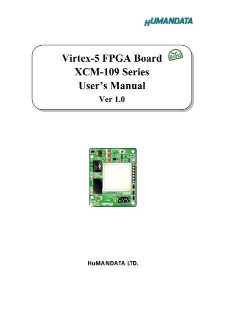
<strong>Virtex</strong>-5 <strong>FPGA</strong> <strong>Board</strong><strong>XCM</strong>-<strong>109</strong> <strong>Series</strong>User’s <strong>Manual</strong>Ver 1.0HuMANDATA LTD.
Table of Contents• Revision History ................................................................................................. 1• Introduction ........................................................................................................ 11. Specifications ......................................................................................................... 22. Overview ................................................................................................................ 32.1. Name of Parts .................................................................................................... 32.2. Block Diagram ................................................................................................... 42.3. Power Supply ..................................................................................................... 42.4. JTAG Connector ................................................................................................. 53. Configuration Switch ............................................................................................. 64. <strong>FPGA</strong> Configuration .............................................................................................. 75. Configuration Device Programming ...................................................................... 76. Additional Documentation and User Support ....................................................... 8
PrecautionsDo Not1. This product uses ordinary off-the-shelf electronic components, and is therefore inappropriate for use inapplications that require special quality or reliability and are expected to protect human lives or preventaccidents, such as safety mechanisms in fields including space, aeronautics, medicine, and nuclearpower.2. Do not be used underwater or in high-humidity environments.3. Do not be used in the presence of corrosive gases, combustible gases, or other flammable gases.4. Do not turn on power when circuit board surface is in contact with other metal.5. Do not apply voltage higher than rated voltage.Attention6. This manual may be revised in the future without notice owing to improvements.7. All efforts have been made to produce the best manual possible, but if users notice an error or otherproblem, we ask that they notify us.8. Item 7 notwithstanding, HuMANDATA cannot be held liable for the consequences arising from use ofthis product.9. HuMANDATA cannot be held liable for consequences arising from using this product in a way differentfrom the uses described herein, or from uses not shown herein.10. This manual, circuit diagrams, sample circuits, and other content may not be copied, reproduced, ordistributed without permission.11. If the product emits smoke, catches fire, or becomes unusually hot, cut the power immediately.12. Be careful of static electricity.13. This product may be subject to the export restrictions of Japan, the United States, or other countries.Purchasers are responsible for properly observing export restrictions.14. HuMANDATA firmly refuses to export (including reexporting) products to countries or regions subject toexport restrictions.Product Warranty and Scope of Support1. HuMANDATA guarantees that its products can be assembled as shown in published circuit diagrams and other design documents.There may be differences between actual components or their prescribed quantities and model numbers and those shown in circuitdiagrams.2. Except for the guarantee in item 1, above, no guarantees whatsoever are made. When assembling the product as shown in a circuitdiagram is impossible, and the problem can be solved by revising the diagram, HuMANDATA will revise the diagram. When aproblem can be solved only by replacing components or modifying the product, HuMANDATA will take back the product to replace itwith a properly functioning product.3. If the problem is minor, HuMANDATA will sometimes describe how to make the revision or modification, and ask the customer tosolve the problem.4. HuMANDATA will determine how to honor the warranty, as through repair, replacement, return, or other action. The customer cannotspecify what action to take.5. <strong>FPGA</strong>s and other components used in products sometimes have characteristic defects. Returns and replacements are not possibleeven if such defects are discovered, whether before or after purchase.6. HuMANDATA shall not be obligated to inform customers about defects in the main components used in products.7. HuMANDATA shall not be obligated to provide support for products, or to provide support for the software of other companiesneeded to use HuMANDATA products.8. Published documentation shall be limited to that published by HuMANDATA at the time of product purchase, and HuMANDATA shallnot be obligated to provide any other documentation.9. When repairs or replacements are provided under warranty in Japan, purchaser shall pay shipping charges for shipping toHuMANDATA, and HuMANDATA shall pay shipping charges for shipping to purchaser.10. When shipping from outside of Japan, purchaser shall pay all expenses including shipping charges and taxes.11. Under whatever circumstances, HuMANDATA shall provide support for its products for a maximum of one year after shipping fromfactory.12. The Warranty is not applicable and support ends in the event of fire, storm and flood damage, earthquakes, lightning strikes, andother natural disasters, as well as conflict or other occurrences.13. Purchaser is assumed to have read and understood all the above when purchasing a HuMANDATA product.Limitation of Liability1. Purchasers assume all liability associated with the use of this product.2. HuMANDATA assumes no liability whatsoever for any direct, indirect, special, incidental, or consequential damages arising from theuse of this product, even if HuMANDATA has been advised of the possibility of such damage, whether legal or in tort.3. At the time this product is purchased, items 1 and 2 above shall be deemed to have been confirmed by purchaser.Trademarks and Other Considerations1. This manual uses various companies’ trademarks in places.2. HuMANDATA is this company’s registered trademark.HuMANDATA’s Philosophy1. HuMANDATA endeavors to raise product quality. We continually make detailed improvements and adjustments that are not shownin circuit diagrams.2. HuMANDATA actively publishes, on the Web and in other ways, information considered useful to customers. Examples would behow to use <strong>FPGA</strong>s and how to use development tools.3. HuMANDATA makes efforts for the long-term provision of products and for continuing their long-term support.4. Instead of concealing small product problems and documentation errors, HuMANDATA makes them public.5. HuMANDATA abides by Japanese law and its spirit. We make no transactions with purchasers who commit illegal acts.
• Revision HistoryDate Revision DescriptionJun. 30, 2010 v1.0 Initial release• IntroductionThank you for buying our product <strong>XCM</strong>-<strong>109</strong> series.This is an evaluation board equipped with a Xilinx <strong>FPGA</strong> <strong>Virtex</strong>-5, power, reset,and clock circuit and configuration device.It can provide you with very convenient and easy-to-use environment.<strong>XCM</strong>-<strong>109</strong> <strong>Series</strong> v1.01
1. SpecificationsModel Name <strong>XCM</strong>-<strong>109</strong>-LX30 <strong>XCM</strong>-<strong>109</strong>-LX50<strong>FPGA</strong> XC5VLX30-1FFG676C XC5VLX50-1FFG676CConfig. Device M25P16-VMN6P (Numonyx, 16Mbit) *SDRAM MT48LC16M16A2BG-7E (Micron, 256Mb: 4Mb x16 x4 banks) *User I/Os 128User Switch 1User LEDs 2On-<strong>Board</strong> Clock 50 [MHz] (External inputs are available) *Status LEDs 2 (POWER, DONE)Power-On Reset 140 [ms] typ. (Configuration Reset Signal) *JTAG Connector SIL 7-pin socket, 2.54 [mm] pitchPower InputDC 3.3 [V](Internal power is generated by an on-board regulator.)PCB8 Layer FR-4 t1.6 [mm] Immersion goldDimensions1.693" x 2.126" (43 x 54 [mm])Weight23 [g] typ.User I/O Connectors FX10A-80P/8-SV1(71) (Hirose) x 2 *AccessoriesSIL 7-pin header (Mounted) *FX10A-80S/8-SV (71) x2 *RoHS Compliance YES* There may be cases that these parts and specifications are changed.<strong>XCM</strong>-<strong>109</strong> <strong>Series</strong> v1.02
2. Overview2.1. Name of PartsUser SwitchDONE LEDOscillator 50 MHzPower & PORPower LEDUser LEDsJTAGSDRAMSerial I/F<strong>FPGA</strong>Thermal DiodeComponent SideConfig. SWUser I/Os (CNA)Config. DeviceUser I/Os (CNB)Solder Side<strong>XCM</strong>-<strong>109</strong> <strong>Series</strong> v1.03
2.2. Block Diagram3.3V INPUTExternal CLKUser I/Os CNB64 GPIOOscillator50MHzSDRAMMT48LC16M16A2(256Mbit)Power-on ResetMin. 140 msPower Circuit2.5V, 1.0VDONE LED<strong>Virtex</strong>-5XC5VLX30/50-1FFG676CConfig. DeviceM25P16 (16Mbit)MUXJTAGBufferJTAGUser LEDs2Config. SwitchPower LED (3.3V)1User Switch64 GPIOUser I/Os CNAVIO(B) INPUTExternal CLK2.3. Power SupplyThis board operates from external 3.3 [V] input. You can use CNA and CNB toinput external power. The external power supply should be sufficient andstabilized.Internally required 2.5[V] and 1.0[V] are generated by on-boarded regulators.<strong>XCM</strong>-<strong>109</strong> <strong>Series</strong> v1.04
2.4. JTAG ConnectorThis connector is used to configure the <strong>FPGA</strong> and program the configuration devicein-system. Pin assignment is as follows.CN3Signal Name Direction JTAG PinGND I/O 1TCK IN 2TDO OUT 3TMS IN 4VCC(3.3V) OUT(POW) 5TDI IN 6GND I/O 7<strong>XCM</strong>-<strong>109</strong> <strong>Series</strong> v1.05
3. Configuration SwitchSW1No. 1 2 3 4 5 6 7 8Net Label FS0 FS1 FS2 HSWAP_EN X_M2 X_M1 X_M0 X_PROGDefault OFF OFF OFF OFF OFF OFF OFF OFFFunction SPI variant sel IO Pull-up Mode Select Target sel.Master SPI Slave Serial JTAGX_M[ 2..0] 0 : 0 : 1 1 : 1 : 1 1 : 0 : 1• FS0, FS1, FS2SPI variant select pins.• HSWAP_ENI/O pull-up control during configuration.ON : pull-upOFF : 3-stated.• M2, M1, M0Configuration mode setting. The modes showed above are compartment.• X_PROGSelect JTAG access target.ON : Configuration deviceOFF : <strong>FPGA</strong><strong>XCM</strong>-<strong>109</strong> <strong>Series</strong> v1.06
4. <strong>FPGA</strong> ConfigurationTo configure the <strong>FPGA</strong> via JTAG, please refer to the following steps.1. Double-click [Configuration Target Device] in [Processes] tab.2. Select [Configure devices using Boundary-Scan (JTAG)].3. Open the bit file you made.4. Confirm [Verify] is not checked in [Device Programming Properties] dialog.5. Select the <strong>FPGA</strong> icon, then open [Operations] menu and click [Program].If configuration is completed successfully, the DONE LED will light up.5. Configuration Device ProgrammingTo program the configuration device via JTAG , you need to prepare mcs file. Youcan generate mcs file using iMPACT. Please refer to the following steps.• Generating mcs file1. Double-click [PROM File Formatter] in [Configuration Modes] tab.2. Select [3rd-Party SPI PROM] for target and choose [MCS] for PROM FileFormat.3. Enter [PROM File Name].4. [Select SPI PROM Density (bits)] set 16M.5. Open the [.bit file] in [Add device] dialog.6. Open [Operations] and click [Generate File].• Programming Configuration Device7. Click [Boundary Scan] in [Configuration Mode] window.8. Select the configuration device icon, then open [Operations] and click[Program].9. Check [Verify] and [Erase Before Programming] then click [OK].Then it will show you the message “Program Succeeded”.<strong>XCM</strong>-<strong>109</strong> <strong>Series</strong> v1.07
6. Additional Documentation and User SupportThe following documents and other supports are available athttp://www.hdl.co.jp/en/spc/<strong>XCM</strong>/xcm-<strong>109</strong>/• Circuit Schematic• Pin List• Dimensional drawing• PCB drawing• Net List… and more.<strong>XCM</strong>-<strong>109</strong> <strong>Series</strong> v1.08
<strong>Virtex</strong>-5 <strong>FPGA</strong> <strong>Board</strong><strong>XCM</strong>-<strong>109</strong> <strong>Series</strong>User’s <strong>Manual</strong>Ver. 1.0 .............................................. Jun. 30, 2010HuMANDATA LTD.Address:Tel:Fax:URL:1-2-10-2F, Nakahozumi, IbarakiOsaka, JapanZIP 567-003481-(0)72-620-2002 (Japanese)81-(0)72-620-2003 (Japanese/English)http://www.hdl.co.jp/en/ (Global)http://www.hdl.co.jp/ (Japan)