COPY DO NOT COPY DO NOT COPY DO NOT COPY
COPY DO NOT COPY DO NOT COPY DO NOT COPY
COPY DO NOT COPY DO NOT COPY DO NOT COPY
- No tags were found...

You also want an ePaper? Increase the reach of your titles
YUMPU automatically turns print PDFs into web optimized ePapers that Google loves.
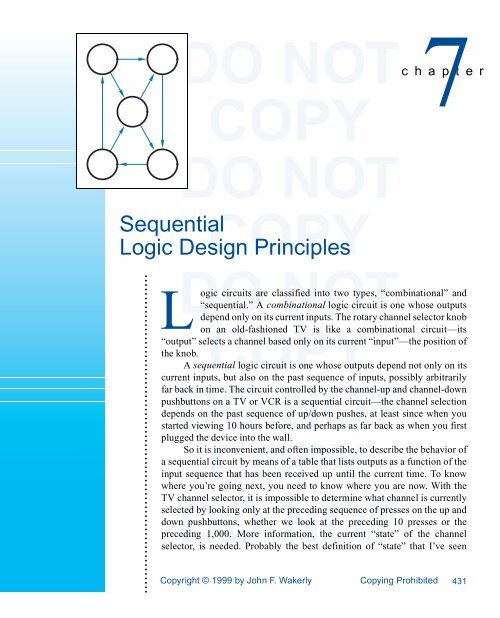
<strong>DO</strong> <strong>NOT</strong><strong>COPY</strong><strong>DO</strong> <strong>NOT</strong><strong>COPY</strong>SequentialLogic Design Principles7c h a p t e r• • • • • • • • • • • • • • • • • • • • • • • • • • • • • • • • • • • • • • • • • • • • • • • • • • • • • • • • • • • • • • • • • • • • • • • •L<strong>DO</strong><strong>NOT</strong><strong>COPY</strong><strong>DO</strong> <strong>NOT</strong><strong>COPY</strong><strong>DO</strong> <strong>NOT</strong>ogic circuits are classified into two types, “combinational” and“sequential.” A combinational logic circuit is one whose outputsdepend only on its current inputs. The rotary channel selector knobon an old-fashioned TV is like a combinational circuit—its“output” selects a channel based only on its current “input”—the position ofthe knob.A sequential logic circuit is one whose outputs depend not only on itscurrent inputs, but also on the past sequence of inputs, possibly arbitrarilyfar back in time. The circuit controlled by the channel-up and channel-downpushbuttons on a TV or VCR is a sequential circuit—the channel selectiondepends on the past sequence of up/down pushes, at least since when youstarted viewing 10 hours before, and perhaps as far back as when you firstplugged the device into the wall.So it is inconvenient, and often impossible, to describe the behavior ofa sequential circuit by means of a table that lists outputs as a function of theinput sequence that has been received up until the current time. To knowwhere you’re going next, you need to know where you are now. With theTV channel selector, it is impossible to determine what channel is currentlyselected by looking only at the preceding sequence of presses on the up anddown pushbuttons, whether we look at the preceding 10 presses or thepreceding 1,000. More information, the current “state” of the channelselector, is needed. Probably the best definition of “state” that I’ve seenCopyright © 1999 by John F. WakerlyCopying Prohibited431
432 Chapter 7 Sequential Logic Design Principles<strong>DO</strong>appeared<strong>NOT</strong>in Herbert Hellerman’s book<strong>COPY</strong>on Digital Computer System Principles(McGraw-Hill, 1967):stateThe state of a sequential circuit is a collection of state variables whosestate variablevalues at any one time contain all the information about the past necessary<strong>DO</strong> <strong>NOT</strong>to account for the circuit’s future<strong>COPY</strong>behavior.In the channel-selector example, the current channel number is the currentstate. Inside the TV, this state might be stored as seven binary state variablesrepresenting a decimal number between 0 and 127. Given the current state<strong>DO</strong>(channel<strong>NOT</strong>number), we can always predict<strong>COPY</strong>the next state as a function of the inputs(presses of the up/down pushbuttons). In this example, one highly visible outputof the sequential circuit is an encoding of the state itself—the channel-numberdisplay. Other outputs, internal to the TV, may be combinational functions of thestate alone (e.g., VHF/UHF/cable tuner selection) or of both state and input<strong>DO</strong>(e.g.,<strong>NOT</strong>turning off the TV if the current<strong>COPY</strong>state is 0 and the “down” button ispressed).State variables need not have direct physical significance, and there areoften many ways to choose them to describe a particular sequential circuit. Forexample, in the TV channel selector, the state might be stored as three BCD<strong>DO</strong>digits<strong>NOT</strong>or 12 bits, with many of the<strong>COPY</strong>bit combinations (4,096 possible) goingunused.In a digital logic circuit, state variables are binary values, corresponding tocertain logic signals in the circuit, as we’ll see in later sections. A circuit with nbinary state variables has 2 n possible states. As large as it might be, 2 n is always<strong>DO</strong> <strong>NOT</strong> <strong>COPY</strong>finite-state machine finite, never infinite, so sequential circuits are sometimes called finite-statemachines.The state changes of most sequential circuits occur at times specified by aclockfree-running clock signal. Figure 7-1 gives timing diagrams and nomenclature<strong>DO</strong>for<strong>NOT</strong>typical clock signals. By convention,<strong>COPY</strong>a clock signal is active high if statechanges occur at the clock’s rising edge or when the clock is HIGH, and activeclock periodlow in the complementary case. The clock period is the time between successiveclock frequency transitions in the same direction, and the clock frequency is the reciprocal of theclock tickperiod. The first edge or pulse in a clock period or sometimes the period itself isduty<strong>DO</strong>cyclecalled<strong>NOT</strong>a clock tick. The duty cycle is the<strong>COPY</strong>percentage of time that the clock signalNON-FINITE- A group of mathematicians recently proposed a non-finite-state machine, but they’reSTATE<strong>DO</strong>MACHINES still<strong>NOT</strong>busy listing its states. . . . Sorry, that’s<strong>COPY</strong>just a joke. There are mathematical modelsfor infinite-state machines, such as Turing machines. They typically contain asmall finite-state-machine control unit, and an infinite amount of auxiliary memory,such as an endless tape.Copyright © 1999 by John F. WakerlyCopying Prohibited
Section 7.1 Bistable Elements 433<strong>DO</strong> <strong>NOT</strong> <strong>COPY</strong>(a)state changes occur hereCLKt<strong>DO</strong> <strong>NOT</strong>Ht Lperiod = t<strong>COPY</strong>pert perfrequency = 1 / t perduty cycle = t H / t per(b)state changes occur hereFigure 7-1CLK_LClock signals:<strong>DO</strong> <strong>NOT</strong> <strong>COPY</strong>t L t H(a) active high;t perduty cycle = t L / t per(b) active low.is at its asserted level. Typical digital systems, from digital watches to supercomputers,<strong>DO</strong>use a quartz-crystal<strong>NOT</strong>oscillator to generate a free-running<strong>COPY</strong>clock signal.Clock frequencies might range from 32.768 kHz (for a watch) to 500 MHz (for aCMOS RISC microprocessor with a cycle time of 2 ns); “typical” systems usingTTL and CMOS parts have clock frequencies in the 5–150 MHz range.In this chapter we’ll discuss two types of sequential circuits that accountfor<strong>DO</strong>the majority of practical discrete<strong>NOT</strong>designs. A feedback sequential<strong>COPY</strong>circuit uses feedback sequentialordinary gates and feedback loops to obtain memory in a logic circuit, thereby circuitcreating sequential-circuit building blocks such as latches and flip-flops that areused in higher-level designs. A clocked synchronous state machine uses these clocked synchronousbuilding blocks, in particular edge-triggered D flip-flops, to create circuits state machinewhose<strong>DO</strong>inputs are examined<strong>NOT</strong>and whose outputs change in accordance<strong>COPY</strong>with acontrolling clock signal. There are other sequential circuit types, such as generalfundamental mode, multiple pulse mode, and multiphase circuits, which aresometimes useful in high-performance systems and VLSI, and are discussed inadvanced texts.<strong>DO</strong> <strong>NOT</strong> <strong>COPY</strong>7.1 Bistable ElementsThe simplest sequential circuit consists of a pair of inverters forming a feedbackloop, as shown in Figure 7-2. It has no inputs and two outputs, Q and Q_L.<strong>DO</strong> <strong>NOT</strong> <strong>COPY</strong>7.1.1 Digital AnalysisThe circuit of Figure 7-2 is often called a bistable, since a strictly digital analysis bistableshows that it has two stable states. If Q is HIGH, then the bottom inverter has aHIGH<strong>DO</strong>input and a LOW output,<strong>NOT</strong>which forces the top inverter’s<strong>COPY</strong>output HIGH aswe assumed in the first place. But if Q is LOW, then the bottom inverter has aLOW input and a HIGH output, which forces Q LOW, another stable situation.We could use a single state variable, the state of signal Q, to describe the state ofthe circuit; there are two possible states, Q = 0 and Q = 1.Copyright © 1999 by John F. WakerlyCopying Prohibited
434 Chapter 7 Sequential Logic Design Principles<strong>DO</strong> <strong>NOT</strong> <strong>COPY</strong>V in1 V out1QFigure 7-2A pair of inverters formingV V<strong>DO</strong> <strong>NOT</strong>a bistable element.<strong>COPY</strong>in2out2Q_LThe bistable element is so simple that it has no inputs and therefore no wayof controlling or changing its state. When power is first applied to the circuit, it<strong>DO</strong>randomly<strong>NOT</strong>comes up in one state or<strong>COPY</strong>the other and stays there forever. Still, itserves our illustrative purposes very well, and we will actually show a couple ofapplications for it in Sections 8.2.3 and 8.2.4.7.1.2 Analog Analysis<strong>DO</strong>The<strong>NOT</strong>analysis of the bistable has more<strong>COPY</strong>to reveal if we consider its operation froman analog point of view. The dark line in Figure 7-3 shows the steady-state (DC)transfer function T for a single inverter; the output voltage is a function of inputvoltage, V<strong>DO</strong> <strong>NOT</strong>out = T(V in ). With two inverters connected in a feedback loop as inFigure 7-2, we know that V in1 = V out2 and V<strong>COPY</strong>in2 = V out1 ; therefore, we can plot thetransfer functions for both inverters on the same graph with an appropriatelabeling of the axes. Thus, the dark line is the transfer function for the topinverter in Figure 7-2, and the colored line is the transfer function for the bottomone.Considering only the steady-state behavior of the bistable’s feedback loop,<strong>DO</strong> <strong>NOT</strong> <strong>COPY</strong>and not dynamic effects, the loop is in equilibrium if the input and outputvoltages of both inverters are constant DC values consistent with the loopconnection and the inverters’ DC transfer function. That is, we must haveV<strong>DO</strong> <strong>NOT</strong>in1 = V<strong>COPY</strong>out2= T(V in2 )= T(V out1 )= T(T(V<strong>DO</strong> <strong>NOT</strong> <strong>COPY</strong>in1 ))VstableFigure 7-3out1= VTransfer functions forin2inverters in a bistablemetastableTransfer function:feedback loop.<strong>DO</strong> <strong>NOT</strong> <strong>COPY</strong>V out1 = T(V in1 )V out2 = T(V in2 )stableV in1 = V out2Copyright © 1999 by John F. WakerlyCopying Prohibited
Section 7.1 Bistable Elements 435Likewise,<strong>DO</strong>we must have<strong>NOT</strong> <strong>COPY</strong>V in2 = T(T(V in2 ))We can find these equilibrium points graphically from Figure 7-3; they are thepoints at which the two transfer curves meet. Surprisingly, we find that there arenot<strong>DO</strong>two but three equilibrium<strong>NOT</strong>points. Two of them, labeled stable,<strong>COPY</strong>correspond to stablethe two states that our “strictly digital” analysis identified earlier, with Q either0 (LOW) or 1 (HIGH).The third equilibrium point, labeled metastable, occurs with V<strong>DO</strong> <strong>NOT</strong> <strong>COPY</strong>out1 and V out2 metastableabout halfway between a valid logic 1 voltage and a valid logic 0 voltage; so Qand Q_L are not valid logic signals at this point. Yet the loop equations aresatisfied; if we can get the circuit to operate at the metastable point, it couldtheoretically stay there indefinitely.7.1.3 Metastable BehaviorCloser<strong>DO</strong>analysis of the situation<strong>NOT</strong>at the metastable point shows<strong>COPY</strong>that it is aptlynamed. It is not truly stable, because random noise will tend to drive a circuitthat is operating at the metastable point toward one of the stable operating pointsas we’ll now demonstrate.Suppose the bistable is operating precisely at the metastable point in<strong>DO</strong> <strong>NOT</strong> <strong>COPY</strong>Figure 7-3. Now let us assume that a small amount of circuit noise reduces V in1by a tiny amount. This tiny change causes V out1 to increase by a small amount.But since V<strong>DO</strong>out1 produces V in2 , we can follow the first horizontal arrow from nearthe metastable point to the second transfer characteristic, which now demands alower voltage for V out2 , which<strong>NOT</strong>is V in1 . Now we’re back where we<strong>COPY</strong>started, exceptwe have a much larger change in voltage at V in1 than the original noise produced,and the operating point is still changing. This “regenerative” process continuesuntil we reach the stable operating point at the upper left-hand corner ofFigure 7-3. However, if we perform a “noise” analysis for either of the stableoperating<strong>DO</strong>points, we find that<strong>NOT</strong>feedback brings the circuit back<strong>COPY</strong>toward the stableoperating point, rather than away from it.Metastable behavior of a bistable can be compared to the behavior of a balldropped onto a hill, as shown in Figure 7-4. If we drop a ball from overhead, itwill probably roll down immediately to one side of the hill or the other. But if itlands<strong>DO</strong>right at the top, it may<strong>NOT</strong>precariously sit there for a while<strong>COPY</strong>before randommetastable<strong>DO</strong> <strong>NOT</strong> <strong>COPY</strong>Figure 7-4Ball and hill analogy forstablestable metastable behavior.Copyright © 1999 by John F. WakerlyCopying Prohibited
436 Chapter 7 Sequential Logic Design Principles<strong>DO</strong>forces<strong>NOT</strong>(wind, rodents, earthquakes) start<strong>COPY</strong>it rolling down the hill. Like the ball atthe top of the hill, the bistable may stay in the metastable state for an unpredictablelength of time before nondeterministically settling into one stable state orthe other.<strong>DO</strong> <strong>NOT</strong>If the simplest sequential circuit<strong>COPY</strong>is susceptible to metastable behavior, youcan be sure that all sequential circuits are susceptible. And this behavior is notsomething that only occurs at power-up.Returning to the ball-and-hill analogy, consider what happens if we try tokick the ball from one side of the hill to the other. Apply a strong force (Arnold<strong>DO</strong>Schwarzenegger),<strong>NOT</strong>and the ball goes<strong>COPY</strong>right over the top and lands in a stableresting place on the other side. Apply a weak force (Mr. Rogers), and the ballfalls back to its original starting place. But apply a wishy-washy force (CharlieBrown), and the ball goes to the top of the hill, teeters, and eventually falls backto one side or the other.<strong>DO</strong> <strong>NOT</strong>This behavior is completely analogous<strong>COPY</strong>to what happens to flip-flops undermarginal triggering conditions. For example, we’ll soon study S-R flip-flops,where a pulse on the S input forces the flip-flop from the 0 state to the 1 state. Aminimum pulse width is specified for the S input. Apply a pulse of this width orlonger, and the flip-flop immediately goes to the 1 state. Apply a very short<strong>DO</strong>pulse,<strong>NOT</strong>and the flip-flop stays in the 0 state.<strong>COPY</strong>Apply a pulse just under the minimumwidth, and the flip-flop may go into the metastable state. Once the flip-flop is inthe metastable state, its operation depends on “the shape of its hill.” Flip-flopsbuilt from high-gain, fast technologies tend to come out of metastability fasterthan ones built from low-performance technologies.<strong>DO</strong> <strong>NOT</strong> <strong>COPY</strong>We’ll say more about metastability in the next section in connection withspecific flip-flop types, and in Section 8.9 with respect to synchronous designmethodology and synchronizer failure.<strong>DO</strong>7.2<strong>NOT</strong>Latches and Flip-Flops<strong>COPY</strong>Latches and flip-flops are the basic building blocks of most sequential circuits.Typical digital systems use latches and flip-flops that are prepackaged, functionallyspecified devices in a standard integrated circuit. In ASIC design<strong>DO</strong>environments,<strong>NOT</strong>latches and flip-flops<strong>COPY</strong>are typically predefined cells specified bythe ASIC vendor. However, within a standard IC or an ASIC, each latch or flipflopcell is typically designed as a feedback sequential circuit using individuallogic gates and feedback loops. We’ll study these discrete designs for tworeasons—to understand the behavior of the prepackaged elements better, and to<strong>DO</strong>gain<strong>NOT</strong>the capability of building a latch<strong>COPY</strong>or flip-flop “from scratch” as is requiredoccasionally in digital-design practice and often in digital-design exams.flip-flopAll digital designers use the name flip-flop for a sequential device that normallysamples its inputs and changes its outputs only at times determined by alatchclocking signal. On the other hand, most digital designers use the name latch forCopyright © 1999 by John F. WakerlyCopying Prohibited
Section 7.2 Latches and Flip-Flops 437<strong>DO</strong> <strong>NOT</strong> <strong>COPY</strong>RS R Q QNQ0 0 last Q last QN Figure 7-50 1 0 1 S-R latch: (a) circuit1 0 1 0 design using NOR<strong>DO</strong> <strong>NOT</strong>QN1 1<strong>COPY</strong>0 0 gates; (b) functionS(a)(b)table.a sequential device that watches all of its inputs continuously and changes itsoutputs at any time, independent of a clocking signal. We follow this standardconvention<strong>DO</strong>in this text. However,<strong>NOT</strong>some textbooks and digital<strong>COPY</strong>designers may(incorrectly) use the name “flip-flop” for a device that we call a “latch.”In any case, because the functional behaviors of latches and flip-flops arequite different, it is important for the logic designer to know which type is beingused in a design, either from the device’s part number (e.g., 74x374 vs. 74x373)<strong>DO</strong> <strong>NOT</strong> <strong>COPY</strong>or other contextual information. We discuss the most commonly used types oflatches and flip-flops in the following subsections.7.2.1 S-R LatchAn<strong>DO</strong>S-R (set-reset) latch based<strong>NOT</strong>on NOR gates is shown in Figure<strong>COPY</strong>7-5(a). The S-R latchcircuit has two inputs, S and R, and two outputs, labeled Q and QN, where QNis normally the complement of Q. Signal QN is sometimes labeled Q or Q_L.If S and R are both 0, the circuit behaves like the bistable element—wehave a feedback loop that retains one of two logic states, Q = 0 or Q = 1. Asshown<strong>DO</strong>in Figure 7-5(b), either<strong>NOT</strong>S or R may be asserted to force<strong>COPY</strong>the feedback loopto a desired state. S sets or presets the Q output to 1; R resets or clears the Q outputto 0. After the S or R input is negated, the latch remains in the state that it was presetsetforced into. Figure 7-6(a) shows the functional behavior of an S-R latch for a resettypical sequence of inputs. Colored arrows indicate causality, that is, which clearinput<strong>DO</strong>transitions cause which<strong>NOT</strong>output transitions.<strong>COPY</strong>S<strong>DO</strong> <strong>NOT</strong> <strong>COPY</strong>RQQN<strong>DO</strong> <strong>NOT</strong> <strong>COPY</strong>(a)(b)Figure 7-6 Typical operation of an S-R latch: (a) “normal” inputs; (b) S and Rasserted simultaneously.Copyright © 1999 by John F. WakerlyCopying Prohibited
438 Chapter 7 Sequential Logic Design Principles<strong>DO</strong> <strong>NOT</strong> <strong>COPY</strong>Q VERSUS QN In most applications of an S-R latch, the QN (a.k.a. Q) output is always the complementof the Q output. However, the Q name is not quite correct, because there is onecase where this output is not the complement of Q. If both S and R are 1, as they are<strong>DO</strong>in several<strong>NOT</strong>places in Figure 7-6(b), then both<strong>COPY</strong>outputs are forced to 0. Once we negateeither input, the outputs return to complementary operation as usual. However, if wenegate both inputs simultaneously, the latch goes to an unpredictable next state, and itmay in fact oscillate or enter the metastable state. Metastability may also occur if a 1pulse that is too short is applied to S or R.<strong>DO</strong> <strong>NOT</strong> <strong>COPY</strong>Three different logic symbols for the same S-R latch circuit are shown inFigure 7-7. The symbols differ in the treatment of the complemented output.Historically, the first symbol was used, showing the active-low or complemented<strong>DO</strong>signal<strong>NOT</strong>name inside the function rectangle.<strong>COPY</strong>However, in bubble-to-bubble logicdesign the second form of the symbol is preferred, showing an inversion bubbleoutside the function rectangle. The last form of the symbol is obviously wrong.propagation delayFigure 7-8 defines timing parameters for an S-R latch. The propagationdelay is the time it takes for a transition on an input signal to produce a transition<strong>DO</strong> <strong>NOT</strong> <strong>COPY</strong>on an output signal. A given latch or flip-flop may have several different propagationdelay specifications, one for each pair of input and output signals. Also,the propagation delay may be different depending on whether the output makesa LOW-to-HIGH or HIGH-to-LOW transition. With an S-R latch, a LOW-to-HIGH<strong>DO</strong>transition<strong>NOT</strong>on S can cause a LOW-to-HIGH<strong>COPY</strong>transition on Q, so a propagation delayt pLH(SQ) occurs as shown in transition 1 in the figure. Similarly, a LOW-to-HIGHtransition on R can cause a HIGH-to-LOW transition on Q, with propagationdelay t<strong>DO</strong> <strong>NOT</strong>pHL(RQ) as shown in transition 2. Not shown in the figure are the correspondingtransitions on QN, which would have propagation delays t<strong>COPY</strong>pHL(SQN) andt pLH(RQN) .minimum pulse width Minimum pulse width specifications are usually given for the S and Rinputs. As shown in Figure 7-8, the latch may go into the metastable state andremain there for a random length of time if a pulse shorter than the minimumwidth t<strong>DO</strong> <strong>NOT</strong>pw(min) is applied to S or R. The latch can be deterministically brought outof the metastable state only by applying<strong>COPY</strong>a pulse to S or R that meets or exceedsthe minimum pulse width requirement.Figure 7-7Symbols for an<strong>DO</strong>S-R latch:<strong>NOT</strong> <strong>COPY</strong>(a) without bubble;S QS QS Q(b) preferred for bubbleto-bubbledesign;R QNR QR QN(c) incorrect becauseof double negation.(a)(b)(c)Copyright © 1999 by John F. WakerlyCopying Prohibited
Section 7.2 Latches and Flip-Flops 439<strong>DO</strong> <strong>NOT</strong> <strong>COPY</strong>HOW CLOSE As mentioned in the previous note, an S-R latch may go into the metastable state ifIS CLOSE? S and R are negated simultaneously. Often, but not always, a commercial latch’sspecifications define “simultaneously” (e.g., S and R negated within 20 ns of each<strong>DO</strong>other).<strong>NOT</strong>In any case, the minimum delay<strong>COPY</strong>between negating S and R for them to beconsidered nonsimultaneous is closely related to the minimum pulse width specification.Both specifications are measures of how long it takes for the latch’s feedbackloop to stabilize during a change of state.SRQ<strong>DO</strong> <strong>NOT</strong> <strong>COPY</strong><strong>DO</strong> <strong>NOT</strong> <strong>COPY</strong>(1)<strong>DO</strong> <strong>NOT</strong> <strong>COPY</strong><strong>DO</strong> <strong>NOT</strong> <strong>COPY</strong><strong>DO</strong> <strong>NOT</strong> <strong>COPY</strong><strong>DO</strong> <strong>NOT</strong> <strong>COPY</strong><strong>DO</strong> <strong>NOT</strong> <strong>COPY</strong>t pLH(SQ)(2)t pHL(RQ)t pw(min)Figure 7-8 Timing parameters for an S-R latch.7.2.2 S-R LatchAn S-R latch (read “S-bar-R-bar latch”) with active-low set and reset inputs maybe built from NAND gates as shown in Figure 7-9(a). In TTL and CMOS logicfamilies, S-R latches are used much more often than S-R latches because NANDgates are preferred over NOR gates.As shown by the function table, Figure 7-9(b), operation of the S-R latch issimilar to that of the S-R, with two major differences. First, S and R are activelow, so the latch remembers its previous state when S = R = 1; the active-lowinputs are clearly indicated in the symbols in (c). Second, when both S and R areasserted simultaneously, both latch outputs go to 1, not 0 as in the S-R latch.Except for these differences, operation of the S-R is the same as the S-R, includingtiming and metastability considerations.(a) S_L(b) (c)S_L R_L Q QNor SQ0 0 1 10 1 1 01 0 0 1R_LQN1 1 last Q last QNS-R latchFigure 7-9 S-R latch: (a) circuit design using NAND gates; (b) function table; (c) logic symbol.or RSRQQCopyright © 1999 by John F. WakerlyCopying Prohibited
440 Chapter 7 Sequential Logic Design Principles<strong>DO</strong> <strong>NOT</strong> <strong>COPY</strong>(a) S(b)(c)S R C Q QNQS0 0 1 last Q last QNQCC0 1 1 0 1QR1 0 1 1 0<strong>DO</strong> <strong>NOT</strong> <strong>COPY</strong>QN1 1 1 1 1Rx x 0 last Q last QNFigure 7-10 S-R latch with enable: (a) circuit using NAND gates; (b) functiontable; (c) logic symbol.<strong>DO</strong> <strong>NOT</strong> <strong>COPY</strong>7.2.3 S-R Latch with EnableAn S-R or S-R latch is sensitive to its S and R inputs at all times. However, itmay easily be modified to create a device that is sensitive to these inputs onlyS-R latch with enable when an enabling input C is asserted. Such an S-R latch with enable is shown in<strong>DO</strong> <strong>NOT</strong> <strong>COPY</strong>Figure 7-10. As shown by the function table, the circuit behaves like an S-Rlatch when C is 1, and retains its previous state when C is 0. The latch’s behaviorfor a typical set of inputs is shown in Figure 7-11. If both S and R are 1 when Cchanges from 1 to 0, the circuit behaves like an S-R latch in which S and R are<strong>DO</strong>negated<strong>NOT</strong>simultaneously—the next state<strong>COPY</strong>is unpredictable and the output maybecome metastable.7.2.4 D LatchS-R latches are useful in control applications, where we often think in terms of<strong>DO</strong>setting<strong>NOT</strong>a flag in response to some condition,<strong>COPY</strong>and resetting it when conditionschange; so we control the set and reset inputs somewhat independently. However,we often need latches simply to store bits of information—each bit ofinformation is presented on a signal line, and we’d like to store it somewhere. AD latchD latch may be used in such an application.<strong>DO</strong> <strong>NOT</strong>Figure 7-12 shows a D latch. Its<strong>COPY</strong>logic diagram is recognizable as that of anS-R latch with enable, with an inverter added to generate S and R inputs from theFigure 7-11 Typical operation of an S-R latch with enable.<strong>DO</strong>Ignored since<strong>NOT</strong>C is 0. Ignored until C<strong>COPY</strong>is 1.SR<strong>DO</strong> <strong>NOT</strong> <strong>COPY</strong>CQQNCopyright © 1999 by John F. WakerlyCopying Prohibited
Section 7.2 Latches and Flip-Flops 441<strong>DO</strong> <strong>NOT</strong> <strong>COPY</strong>DQC D Q QNC 1 0 0 1D Q1 1 1 0C Q<strong>DO</strong> <strong>NOT</strong> <strong>COPY</strong>QN 0 x last Q last QN(a)(b)(c)Figure 7-12 D latch: (a) circuit design using NAND gates; (b) function table; (c) logic symbol.DC<strong>DO</strong> <strong>NOT</strong> <strong>COPY</strong>Q<strong>DO</strong> <strong>NOT</strong> <strong>COPY</strong><strong>DO</strong> <strong>NOT</strong> <strong>COPY</strong><strong>DO</strong> <strong>NOT</strong> <strong>COPY</strong><strong>DO</strong> <strong>NOT</strong> <strong>COPY</strong>Figure 7-13 Functional behavior of a D latch for various inputs.single D (data) input. This eliminates the troublesome situation in S-R latches,where S and R may be asserted simultaneously. The control input of a D latch,labeled C in (c), is sometimes named ENABLE, CLK, or G, and is active low insome D-latch designs.An example of a D latch’s functional behavior is given in Figure 7-13.When the C input is asserted, the Q output follows the D input. In this situation,the latch is said to be “open” and the path from D input to Q output is “transparent”;the circuit is often called a transparent latch for this reason. When the Cinput is negated, the latch “closes”; the Q output retains its last value and nolonger changes in response to D, as long as C remains negated.More detailed timing behavior of the D latch is shown in Figure 7-14. Fourdifferent delay parameters are shown for signals that propagate from the C or Dinput to the Q output. For example, at transitions 1 and 4 the latch is initiallyFigure 7-14 Timing parameters for a D latch.transparent latchDCQ<strong>DO</strong> <strong>NOT</strong> <strong>COPY</strong><strong>DO</strong> <strong>NOT</strong> <strong>COPY</strong>(1) (2) (3) (4) (5)t pHL(DQ)t pHL(CQ)t holdt pLH(CQ)t pLH(DQ)t pLH(DQ)t setupCopyright © 1999 by John F. WakerlyCopying Prohibited
442 Chapter 7 Sequential Logic Design Principles<strong>DO</strong>“closed”<strong>NOT</strong>and the<strong>COPY</strong>D input is the opposite of Q output, so that when C goes to 1 thelatch “opens up” and the Q output changes after delay t pLH(CQ) or t pHL(CQ) . Attransitions 2 and 3 the C input is already 1 and the latch is already open, so thatQ transparently follows the transitions on D with delay t<strong>DO</strong> <strong>NOT</strong> <strong>COPY</strong>pHL(DQ) and t pLH(DQ) .Four more parameters specify the delay to the QN output, not shown.Although the D latch eliminates the S = R = 1 problem of the S-R latch, itdoes not eliminate the metastability problem. As shown in Figure 7-14, there isa (shaded) window of time around the falling edge of C when the D input mustnot change. This window begins at time t<strong>DO</strong> <strong>NOT</strong> <strong>COPY</strong>setup before the falling (latching) edgesetup timeof C; t setup is called the setup time. The window ends at time t hold afterward; t holdhold timeis called the hold time. If D changes at any time during the setup- and hold-timewindow, the output of the latch is unpredictable and may become metastable, asshown for the last latching edge in the figure.<strong>DO</strong>7.2.5<strong>NOT</strong>Edge-Triggered D Flip-Flop<strong>COPY</strong>positive-edge-triggered A positive-edge-triggered D flip-flop combines a pair of D latches, as shown inD flip-flopFigure 7-15, to create a circuit that samples its D input and changes its Q and QNoutputs only at the rising edge of a controlling CLK signal. The first latch ismastercalled the master; it is open and follows the input when CLK is 0. When CLK<strong>DO</strong>goes<strong>NOT</strong>to 1, the master latch is closed<strong>COPY</strong>and its output is transferred to the secondslavelatch, called the slave. The slave latch is open all the while that CLK is 1, butchanges only at the beginning of this interval, because the master is closed andunchanging during the rest of the interval.The triangle on the D flip-flop’s CLK input indicates edge-triggered behavior,and is called a dynamic-input indicator. Examples of the flip-flop’s<strong>DO</strong> <strong>NOT</strong> <strong>COPY</strong>dynamic-inputindicatorfunctional behavior for several input transitions are presented in Figure 7-16.The QM signal shown is the output of the master latch. Notice that QM changesonly when CLK is 0. When CLK goes to 1, the current value of QM is transferred<strong>DO</strong>to Q,<strong>NOT</strong>and QM is prevented from changing<strong>COPY</strong>until CLK goes to 0 again.Figure 7-17 shows more detailed timing behavior for the D flip-flop. Allpropagation delays are measured from the rising edge of CLK, since that’s theonly event that causes an output change. Different delays may be specified forLOW-to-HIGH and HIGH-to-LOW output changes.<strong>DO</strong> <strong>NOT</strong> <strong>COPY</strong>Figure 7-15 Positive-edge-triggered D flip-flop: (a) circuit design usingD latches; (b) function table; (c) logic symbol.(a)(b)(c)<strong>DO</strong>D<strong>NOT</strong>QMQ<strong>COPY</strong>D CLK Q QND QD Q0 0 1D QCC Q QN1 1 0CLK Qx 0 last Q last QNCLKx 1 last Q last QNCopyright © 1999 by John F. WakerlyCopying Prohibited
Section 7.2 Latches and Flip-Flops 443<strong>DO</strong> <strong>NOT</strong> <strong>COPY</strong>DCLKQM<strong>DO</strong> <strong>NOT</strong> <strong>COPY</strong>QQN<strong>DO</strong> <strong>NOT</strong> <strong>COPY</strong>Figure 7-16 Functional behavior of a positive-edge-triggered D flip-flop.Like a D latch, the edge-triggered D flip-flop has a setup and hold timewindow during which the D inputs must not change. This window occurs aroundthe<strong>DO</strong>triggering edge of CLK,<strong>NOT</strong>and is indicated by shaded color<strong>COPY</strong>in Figure 7-17. Ifthe setup and hold times are not met, the flip-flop output will usually go to a stable,though unpredictable, 0 or 1 state. In some cases, however, the output willoscillate or go to a metastable state halfway between 0 and 1, as shown at thesecond-to-last clock tick in the figure. If the flip-flop goes into the metastablestate,<strong>DO</strong>it will return to a stable<strong>NOT</strong>state on its own only after a probabilistic<strong>COPY</strong>delay, asexplained in \secref{metest}. It can also be forced into a stable state by applyinganother triggering clock edge with a D input that meets the setup- and hold-timerequirements, as shown at the last clock tick in the figure.A negative-edge-triggered D flip-flop simply inverts the clock input, so negative-edge-triggeredthat<strong>DO</strong>all the action takes place<strong>NOT</strong>on the falling edge of CLK_L;<strong>COPY</strong>by convention, a D flip-flopfalling-edge trigger is considered to be active low. The flip-flop’s function tableand logic symbol are shown in Figure 7-18.Some D flip-flops have asynchronous inputs that may be used to force the asynchronous inputsflip-flop to a particular state independent of the CLK and D inputs. These inputs, preset<strong>DO</strong> <strong>NOT</strong> <strong>COPY</strong>typically labeled PR (preset) and CLR (clear), behave like the set and reset clearFigure 7-17 Timing behavior of a positive-edge-triggered D flip-flop.D<strong>DO</strong> <strong>NOT</strong> <strong>COPY</strong>CLK<strong>DO</strong> <strong>NOT</strong> <strong>COPY</strong>Qt holdt pLH(CQ)t pHL(CQ)t setupCopyright © 1999 by John F. WakerlyCopying Prohibited
444 Chapter 7 Sequential Logic Design Principles<strong>DO</strong> <strong>NOT</strong> <strong>COPY</strong>D CLK_L Q QNDD QD Q Q0 0 1CC Q QN1 1 0D Qx 0<strong>DO</strong> <strong>NOT</strong> <strong>COPY</strong>last Q last QNCLK_LCLK Qx 1 last Q last QN(a)(b)(c)Figure 7-18 Negative-edge triggered D flip-flop: (a) circuit design usingD latches; (b) function table; (c) logic symbol.<strong>DO</strong>inputs<strong>NOT</strong>on an SR latch. The logic symbol<strong>COPY</strong>and NAND circuit for an edge-triggeredD flip-flop with these inputs is shown in Figure 7-19. Although asynchronousinputs are used by some logic designers to perform tricky sequential functions,they are best reserved for initialization and testing purposes, to force a sequentialcircuit into a known starting state; more on this when we discuss synchronous<strong>DO</strong>design<strong>NOT</strong>methodology in \secref{syncmethod}.<strong>COPY</strong>7.2.6 Edge-Triggered D Flip-Flop with EnableA commonly desired function in D flip-flops is the ability to hold the last valuestored, rather than load a new value, at the clock edge. This is accomplished by<strong>DO</strong> <strong>NOT</strong> <strong>COPY</strong>enable inputadding an enable input, called EN or CE (clock enable). While the name “clockclock-enable input enable” is descriptive, the extra input’s function is not obtained by controllingFigure 7-19 Positive-edge-triggered D flip-flop with preset and clear:<strong>DO</strong> <strong>NOT</strong>(a) logic symbol; (b)<strong>COPY</strong>circuit design using NAND gates.(b) PR_LD(a)Q<strong>DO</strong> <strong>NOT</strong> <strong>COPY</strong>PRD QCLK QCLRQN<strong>DO</strong> <strong>NOT</strong> <strong>COPY</strong>CLKCLR_L<strong>DO</strong> <strong>NOT</strong> <strong>COPY</strong>TIME FOR A Commercial TTL positive-edge-triggered D flip-flops do not use the master-slaveCOMMERCIAL latch design of Figure 7-15 or Figure 7-19. Instead, flip-flops like the 74LS74 use thesix-gate design of Figure 7-20, which is smaller and faster. We’ll show how toformally analyze the next-state behavior of both designs in Section 7.9.Copyright © 1999 by John F. WakerlyCopying Prohibited
Section 7.2 Latches and Flip-Flops 445<strong>DO</strong> <strong>NOT</strong> <strong>COPY</strong>PR_L<strong>DO</strong> <strong>NOT</strong> <strong>COPY</strong>CLR_LQ<strong>DO</strong>CLK<strong>NOT</strong> <strong>COPY</strong>QNFigure 7-20Commercial circuit fora positive-edgetriggeredD flip-flopDsuch as 74LS74.<strong>DO</strong> <strong>NOT</strong> <strong>COPY</strong>the clock in any way whatsoever. Rather, as shown in Figure 7-21(a), a 2-inputmultiplexer controls the value applied to the internal flip-flop’s D input. If EN isasserted, the external D input is selected; if EN is negated, the flip-flop’s currentoutput<strong>DO</strong>is used. The resulting<strong>NOT</strong>function table is shown in (b). The<strong>COPY</strong>flip-flop symbolis shown in (c); in some flip-flops, the enable input is active low, denoted by aninversion bubble on this input.7.2.7 Scan Flip-FlopAn<strong>DO</strong>important flip-flop function<strong>NOT</strong>for ASIC testing is so-called<strong>COPY</strong>scan capability. scan capabilityThe idea is to be able to drive the flip-flop’s D input with an alternate source ofdata during device testing. When all of the flip-flops are put into testing mode,a test pattern can be “scanned in” to the ASIC using the flip-flops’ alternate datainputs. After the test pattern is loaded, the flip-flops are put back into “normal”<strong>DO</strong> <strong>NOT</strong> <strong>COPY</strong>mode, and all of the flip-flops are clocked normally. After one or more clockticks, the flip-flops are put back into test mode, and the test results are “scannedout.”Figure<strong>DO</strong>7-21 Positive-edge-triggered<strong>NOT</strong>D flip-flop with enable:<strong>COPY</strong>(a) circuit design;(b) function table; (c) logic symbol.(a)(b)(c)DD EN CLK Q QNEN D Q<strong>DO</strong> <strong>NOT</strong>0<strong>COPY</strong>1 0 1D Q QEN1 1 1 0CLK QC Q QNx 0 last Q last QNCLKx x 0 last Q last QNx x 1 last Q last QNCopyright © 1999 by John F. WakerlyCopying Prohibited
446 Chapter 7 Sequential Logic Design Principles<strong>DO</strong> <strong>NOT</strong> <strong>COPY</strong>TE TI D CLK Q QNDTE 0 x 0 0 1DQD Q Q 0 x 1 1 0TEC Q QN 1 0 x 0 1<strong>DO</strong>TI<strong>NOT</strong> <strong>COPY</strong>TI1 1 x 1 0QCLKCLKx x x 0 last Q last QNx x x 1 last Q last QN(a)(b)(c)Figure 7-22 Positive-edge-triggered<strong>DO</strong> <strong>NOT</strong> <strong>COPY</strong>D flip-flop with scan: (a) circuit design;(b) function table; (c) logic symbol.Figure 7-22(a) shows the design of a typical scan flip-flop. It is nothingmore than a D flip-flop with a 2-input multiplexer on the D input. When the TEtest-enable (test enable) input is negated, the circuit behaves like an ordinary<strong>DO</strong>input, TE<strong>NOT</strong> <strong>COPY</strong>D flip-flop.test input, TIWhen TE is asserted, it takes its data from TI (test input) instead of from D. Thisfunctional behavior is shown in (b), and a symbol for the device is given in (c).scan chainThe extra inputs are used to connect all of an ASIC’s flip-flops in a scanchain for testing purposes. Figure 7-23 is a simple example with four flip-flops<strong>DO</strong>in the<strong>NOT</strong>scan chain. The TE inputs of all<strong>COPY</strong>the flip-flops are connected to a global TEinput, while each flip-flop’s Q output is connected to another’s TI input in serial(daisy-chain) fashion. The TI, TE, and TO (test output) connections are strictlyfor testing purposes; the additional logic connected to the D inputs and Q outputsneeded to make the circuit do something useful are not shown.<strong>DO</strong> <strong>NOT</strong>To test the circuit, including the<strong>COPY</strong>additional logic, the global TE input isasserted while n clock ticks occur and n test-vector bits are applied to the globalTI input and are thereby scanned (shifted) into the n flip-flops; n equals 4 inFigure 7-23. Then TE is negated, and the circuit is allowed to run for one or moreadditional clock ticks. The new state of the circuit, represented by the new values<strong>DO</strong>in the<strong>NOT</strong>n flip-flops, can be observed (scanned<strong>COPY</strong>out) at TO by asserting TE while nmore clock ticks occur. To make the testing process more efficient, another testvector can be scanned in while the previous result is being scanned out.ASICFigure 7-23 A scan chain with four flip-flops.external<strong>DO</strong> <strong>NOT</strong> <strong>COPY</strong>pinsDDDDQQQQTETETETE<strong>DO</strong>TI<strong>NOT</strong> <strong>COPY</strong>TITITITITOQQQQCLKCLKCLKCLKCLKTECopyright © 1999 by John F. WakerlyCopying Prohibited
Section 7.2 Latches and Flip-Flops 447<strong>DO</strong>There are many different<strong>NOT</strong>types of scan flip-flops, corresponding<strong>COPY</strong>to differenttypes of basic flip-flop functionality. For example, scan capability could beadded to the D flip-flop with enable in Figure 7-21, by replacing its internal2-input multiplexer with a 3-input one. At each clock tick, the flip-flop wouldload<strong>DO</strong>D, TI, or its current state<strong>NOT</strong>depending on the values of EN and<strong>COPY</strong>TE. Scan capabilitycan also be added to other flip-flop types, such as J-K and T introducedlater in this section.*7.2.8 Master/Slave S-R Flip-FlopWe<strong>DO</strong>indicated earlier that S-R<strong>NOT</strong>latches are useful in “control” applications,<strong>COPY</strong>wherewe may have independent conditions for setting and resetting a control bit. If thecontrol bit is supposed to be changed only at certain times with respect to a clocksignal, then we need an S-R flip-flop that, like a D flip-flop, changes its outputsonly on a certain edge of the clock signal. This subsection and the next twodescribe<strong>DO</strong>flip-flops that are useful<strong>NOT</strong>for such applications.<strong>COPY</strong>If we substitute S-R latches for the D latches in the negative-edge-triggeredD flip-flop of Figure 7-18(a), we get a master/slave S-R flip-flop, shown in master/slave S-RFigure 7-24. Like a D flip-flop, the S-R flip-flop changes its outputs only at the flip-flopfalling edge of a control signal C. However, the new output value depends oninput<strong>DO</strong>values not just at the falling<strong>NOT</strong>edge, but during the entire interval<strong>COPY</strong>in which Cis 1 prior to the falling edge. As shown in Figure 7-25, a short pulse on S anytime during this interval can set the master latch; likewise, a pulse on R can resetit. The value transferred to the flip-flop output on the falling edge of C dependson whether the master latch was last set or cleared while C was 1.<strong>DO</strong> <strong>NOT</strong> <strong>COPY</strong>Shown in Figure 7-24(c), the logic symbol for the master/slave S-R flipflopdoes not use a dynamic-input indicator, because the flip-flop is not trulyedge triggered. It is more like a latch that follows its input during the entire intervalthat C is 1, but that changes its output to reflect the final latched value onlywhen<strong>DO</strong>C goes to 0. In the symbol,<strong>NOT</strong>a postponed-output indicator<strong>COPY</strong>indicates that the postponed-outputoutput signal does not change until enable input C is negated. Flip-flops with this indicatorkind of behavior are sometimes called pulse-triggered flip-flops.pulse-triggeredflip-flopFigure 7-24 Master/slave S-R flip-flop: (a) circuit using S-R latches;(b) function table; (c) logic symbol.<strong>DO</strong> <strong>NOT</strong> <strong>COPY</strong>(a)(b)(c)S R C Q QNSS QMQSQSQx x 0 last Q last QNQC QM_L CCQQ QN 0 0 last Q last QNQRRRR<strong>DO</strong> <strong>NOT</strong>0 1<strong>COPY</strong>0 1C1 0 1 01 1 undef. undef.*Throughout this book, optional sections are marked with an asterisk.Copyright © 1999 by John F. WakerlyCopying Prohibited
448 Chapter 7 Sequential Logic Design Principles<strong>DO</strong> <strong>NOT</strong> <strong>COPY</strong>Ignored since C is 0. Ignored until C is 1. Ignored until C is 1.SR<strong>DO</strong> <strong>NOT</strong> <strong>COPY</strong>CQMQM_L<strong>DO</strong> <strong>NOT</strong> <strong>COPY</strong>QQN<strong>DO</strong> <strong>NOT</strong> <strong>COPY</strong>Figure 7-25 Internal and functional behavior of a master/slave S-R flip-flop.The operation of the master/slave S-R flip-flop is unpredictable if both Sand R are asserted at the falling edge of C. In this case, just before the falling<strong>DO</strong>edge,<strong>NOT</strong>both the Q and QN outputs of the<strong>COPY</strong>master latch are 1. When C goes to 0, themaster latch’s outputs change unpredictably and may even become metastable.At the same time, the slave latch opens up and propagates this garbage to theflip-flop output.<strong>DO</strong>*7.2.9<strong>NOT</strong>Master/Slave J-K Flip-Flop<strong>COPY</strong>The problem of what to do when S and R are asserted simultaneously is solvedmaster/slave J-K flipflopHowever, as shown in Figure 7-26, asserting J asserts the master’s S input onlyin a master/slave J-K flip-flop. The J and K inputs are analogous to S and R.if the flip-flop’s QN output is currently 1 (i.e., Q is 0), and asserting K asserts the<strong>DO</strong> <strong>NOT</strong> <strong>COPY</strong>master’s R input only if Q is currently 1. Thus, if J and K are asserted simultaneously,the flip-flop goes to the opposite of its current state.Figure 7-26 Master/slave J-K flip-flop: (a) circuit design using S-R latches;<strong>DO</strong> <strong>NOT</strong>(b) function table; (c)<strong>COPY</strong>logic symbol.(a)(b)(c)J K C Q QNJQJS QM SQQ Q x x 0 last Q last QNC<strong>DO</strong>C<strong>NOT</strong>C<strong>COPY</strong>QQM_L0 0 last Q last QNKKQQRRQN0 1 0 11 0 1 0C1 1 last QN last QCopyright © 1999 by John F. WakerlyCopying Prohibited
Section 7.2 Latches and Flip-Flops 449<strong>DO</strong> <strong>NOT</strong> <strong>COPY</strong>IgnoredIgnoredIgnoredIgnoredIgnoredsince C is 0. since QN is 0. since C is now 0. since Q is 0. since QN is 0.J<strong>DO</strong>K<strong>NOT</strong> <strong>COPY</strong>CQM<strong>DO</strong> <strong>NOT</strong> <strong>COPY</strong>QM_LQQN<strong>DO</strong> <strong>NOT</strong> <strong>COPY</strong>Figure 7-27 Internal and functional behavior of a master/slave J-K flip-flop.Figure 7-27 shows the functional behavior of a J-K master/slave flip-flopfor a typical set of inputs. Note that the J and K inputs need not be asserted at theend<strong>DO</strong>of the triggering pulse for<strong>NOT</strong>the flip-flop output to change at<strong>COPY</strong>that time. In fact,because of the gating on the master latch’s S and R inputs, it is possible for theflip-flop output to change to 1 even though K and not J is asserted at the end ofthe triggering pulse. This behavior, known as 1s catching, is illustrated in the 1s catchingsecond-to-last triggering pulse in the figure. An analogous behavior known as 0scatching<strong>DO</strong>is illustrated in the last<strong>NOT</strong>triggering pulse. Because of this<strong>COPY</strong>behavior, the J 0s catchingand K inputs of a J-K master/slave flip-flop must be held valid during the entireinterval that C is 1.7.2.10 Edge-Triggered J-K Flip-FlopThe<strong>DO</strong>problem of 1s and 0s catching<strong>NOT</strong>is solved in an edge-triggered<strong>COPY</strong>J-K flip-flop, edge-triggered J-Kwhose functional equivalent is shown in Figure 7-28. Using an edge-triggered D flip-flopflip-flop internally, the edge-triggered J-K flip-flop samples its inputs at theFigure 7-28 Edge-triggered J-K flip-flop: (a) equivalent function using an<strong>DO</strong>edge-triggered<strong>NOT</strong>D flip-flop; (b) function table; (c)<strong>COPY</strong>logic symbol.(a)(b)(c)J K CLK Q QNJx x 0 Qlast Q last QNJCLK<strong>DO</strong> <strong>NOT</strong>D QQ<strong>COPY</strong>x x 1 last Q last QNQKK0 0 last Q last QNCLK QQN0 1 0 1CLK1 0 1 01 1 last QN last QCopyright © 1999 by John F. WakerlyCopying Prohibited
450 Chapter 7 Sequential Logic Design Principles<strong>DO</strong> <strong>NOT</strong> <strong>COPY</strong>JKCLK<strong>DO</strong> <strong>NOT</strong> <strong>COPY</strong>QFigure 7-29 Functional behavior of a positive-edge-triggered J-K flip-flop.<strong>DO</strong> <strong>NOT</strong> <strong>COPY</strong>rising edge of the clock and produces its next output according to the “characteristicequation” Q* = J ⋅ Q′ + K′ ⋅ Q (see Section 7.3.3).Typical functional behavior of an edge-triggered J-K flip-flop is shown inFigure 7-29. Like the D input of an edge-triggered D flip-flop, the J and K inputs<strong>DO</strong>of a<strong>NOT</strong>J-K flip-flop must meet published<strong>COPY</strong>setup- and hold-time specifications withrespect to the triggering clock edge for proper operation.Because they eliminate the problems of 1s and 0s catching and of simultaneouslyasserting both control inputs, edge-triggered J-K flip-flops have largely74x109obsoleted the older pulse-triggered types. The 74x109 is a TTL positive-edgetriggered<strong>DO</strong> <strong>NOT</strong>J-K flip-flop with an active-low<strong>COPY</strong>K input (named K or K_L).A<strong>NOT</strong>HER The internal design of the 74LS109 is very similar to that of the 74LS74, which weCOMMERCIAL showed in Figure 7-20. As shown in Figure 7-30, the ’109 simply replaces the<strong>DO</strong>(FLIP-FLOP, bottom-left<strong>NOT</strong>gate of the ’74, which realizes<strong>COPY</strong>the characteristic equation Q* = D, with anTHAT IS) AND-OR structure that realizes the J-K characteristic equation, Q* = J ⋅ Q′ + K_L ⋅ Q.Figure 7-30PR_LInternal<strong>DO</strong>logic diagram<strong>NOT</strong> <strong>COPY</strong>for the 74LS109positive-edge-triggeredJ-K flip-flop.CLR_LQ<strong>DO</strong> <strong>NOT</strong> <strong>COPY</strong>CLKQN<strong>DO</strong> <strong>NOT</strong>J<strong>COPY</strong>K_LCopyright © 1999 by John F. WakerlyCopying Prohibited
Section 7.2 Latches and Flip-Flops 451<strong>DO</strong> <strong>NOT</strong> <strong>COPY</strong>TQTQQ(a)(b)Figure<strong>DO</strong>7-31 Positive-edge-triggered<strong>NOT</strong>T flip-flop: (a) logic symbol;<strong>COPY</strong>(b) functional behavior.The most common application of J-K flip-flops is in clocked synchronousstate machines. As we’ll explain in Section 7.4.5, the next-state logic for J-Kflip-flops is sometimes simpler than for D flip-flops. However, most statemachines<strong>DO</strong>are still designed using<strong>NOT</strong>D flip-flops because the design<strong>COPY</strong>methodology isa bit simpler and because most sequential programmable logic devices containD, not J-K, flip-flops. Therefore, we’ll give most of our attention to D flip-flops.7.2.11 T Flip-Flop<strong>DO</strong> <strong>NOT</strong> <strong>COPY</strong>A T (toggle) flip-flop changes state on every tick of the clock. Figure 7-31 shows T flip-flopthe symbol and illustrates the behavior of a positive-edge-triggered T flip-flop.Notice that the signal on the flip-flop’s Q output has precisely half the frequencyof the T input. Figure 7-32 shows how to obtain a T flip-flop from a D or J-K flipflop.<strong>DO</strong>T flip-flops are most often<strong>NOT</strong>used in counters and frequency<strong>COPY</strong>dividers, as we’llshow in \secref{counters}.In many applications of T flip-flops, the flip-flop need not be toggled onevery clock tick. Such applications can use a T flip-flop with enable. As shown T flip-flop with enablein Figure 7-33, the flip-flop changes state at the triggering edge of the clock onlyif the<strong>DO</strong>enable signal EN is asserted.<strong>NOT</strong>Like the D, J, and K inputs on<strong>COPY</strong>other edge-triggeredflip-flops, the EN input must meet specified setup and hold times withrespect to the triggering clock edge. The circuits of Figure 7-32 are easily modifiedto provide an EN input, as shown in Figure 7-34.<strong>DO</strong> <strong>NOT</strong> <strong>COPY</strong>(a)(b)Figure 7-321 JD QQQ Q Possible circuit designs for aTCLKTCLK QQNQKQNT flip-flop: (a) using a D flipflop;(b) using a J-K flip-flop.<strong>DO</strong> <strong>NOT</strong> <strong>COPY</strong>Figure 7-33 Positive-edge-triggered T flip-flop with enable: (a) logic symbol;(b) functional behavior.(a)(b)<strong>DO</strong> <strong>NOT</strong> <strong>COPY</strong>ENEN QT QTQCopyright © 1999 by John F. WakerlyCopying Prohibited
452 Chapter 7 Sequential Logic Design Principles<strong>DO</strong> <strong>NOT</strong> <strong>COPY</strong>Figure 7-34JD QQENPossible circuits for aQ QENTCLKT flip-flop with enable:CLK QQNQKQN(a) using a D flip-flop; T(b)<strong>DO</strong>using a J-K flip-flop. (a)<strong>NOT</strong> <strong>COPY</strong>(b)7.3 Clocked Synchronous State-Machine Analysis<strong>DO</strong>Although<strong>NOT</strong>latches and flip-flops, the basic<strong>COPY</strong>building blocks of sequential circuits,are themselves feedback sequential circuits that can be formally analyzed, we’llclocked synchronous first study the operation of clocked synchronous state machines, since they arestate machine the easiest to understand. “State machine” is a generic name given to thesesequential circuits; “clocked” refers to the fact that their storage elements (flipflops)<strong>DO</strong> <strong>NOT</strong>employ a clock input; and “synchronous”<strong>COPY</strong>means that all of the flip-flopsuse the same clock signal. Such a state machine changes state only when a triggeringedge or “tick” occurs on the clock signal.7.3.1 State-Machine Structure<strong>DO</strong>Figure<strong>NOT</strong>7-35 shows the general structure<strong>COPY</strong>of a clocked synchronous state machine.state memoryThe state memory is a set of n flip-flops that store the current state of themachine, and has 2 n distinct states. The flip-flops are all connected to a commontickclock signal that causes the flip-flops to change state at each tick of the clock.What constitutes a tick depends on the flip-flop type (edge triggered, pulse triggered,etc.). For the positive-edge-triggered D and J-K flip-flops considered in<strong>DO</strong> <strong>NOT</strong> <strong>COPY</strong>this section, a tick is the rising edge of the clock signal.next-state logicThe next state of the state machine in Figure 7-35 is determined by theoutput logicnext-state logic F as a function of the current state and input. The output logic G<strong>DO</strong> <strong>NOT</strong> <strong>COPY</strong>Figure 7-35 Clocked synchronous state-machine structure (Mealy machine).<strong>DO</strong> <strong>NOT</strong> <strong>COPY</strong>inputsNext-state excitation State current state OutputLogicMemoryLogicoutputsFG<strong>DO</strong> <strong>NOT</strong> <strong>COPY</strong>clock inputclocksignalCopyright © 1999 by John F. WakerlyCopying Prohibited
Section 7.3 Clocked Synchronous State-Machine Analysis 453determines<strong>DO</strong>the output as a function<strong>NOT</strong>of the current state and input.<strong>COPY</strong>Both F and Gare strictly combinational logic circuits. We can writeNext state = F(current state, input)Output = G(current state, input)<strong>DO</strong> <strong>NOT</strong> <strong>COPY</strong>State machines may use positive-edge-triggered D flip-flops for their statememory, in which case a tick occurs at each rising edge of the clock signal. It isalso possible for the state memory to use negative-edge-triggered D flip-flops, Dlatches, or J-K flip-flops. However, inasmuch as most state machines aredesigned<strong>DO</strong>nowadays using programmable<strong>NOT</strong>logic devices with positive-edge-triggeredD flip-flops, that’s what we’ll concentrate on.<strong>COPY</strong>7.3.2 Output LogicA sequential circuit whose output depends on both state and input as shown inFigure<strong>DO</strong>7-35 is called a Mealy<strong>NOT</strong>machine. In some sequential circuits,<strong>COPY</strong>the outputdepends on the state alone:Output = G(current state)Such a circuit is called a Moore machine, and its general structure is shown inFigure<strong>DO</strong>7-36.<strong>NOT</strong> <strong>COPY</strong>Obviously, the only difference between the two state-machine models is inhow outputs are generated. In practice, many state machines must be categorizedas Mealy machines, because they have one or more Mealy-type outputs thatdepend on input as well as state. However, many of these same machines alsohave<strong>DO</strong>one or more Moore-type<strong>NOT</strong>outputs that depend only on state.<strong>COPY</strong>In the design of high-speed circuits, it is often necessary to ensure thatstate-machine outputs are available as early as possible and do not change duringeach clock period. One way to get this behavior is to encode the state so that thestate variables themselves serve as outputs. We call this an output-coded state output-coded stateassignment;<strong>DO</strong>it produces a<strong>NOT</strong>Moore machine in which the<strong>COPY</strong>output logic of assignmentFigure 7-36 is null, consisting of just wires.Figure 7-36 Clocked synchronous state-machine structure (Moore machine).<strong>DO</strong> <strong>NOT</strong> <strong>COPY</strong>inputsNext-state excitation State current state OutputLogicMemoryLogicoutputsFG<strong>DO</strong> <strong>NOT</strong> <strong>COPY</strong>clock inputclocksignalCopyright © 1999 by John F. WakerlyCopying Prohibited
454 Chapter 7 Sequential Logic Design Principles<strong>DO</strong> <strong>NOT</strong> <strong>COPY</strong>inputsNext-state excitation<strong>DO</strong> <strong>NOT</strong>State current state OutputOutputLogic<strong>COPY</strong>MemoryLogicPipelinepipelinedMemoryoutputsFGclock inputclock input<strong>DO</strong> <strong>NOT</strong> <strong>COPY</strong>clocksignalFigure 7-37 Mealy machine with pipelined outputs.<strong>DO</strong> <strong>NOT</strong> <strong>COPY</strong>Another approach is to design the state machine so that the outputs duringone clock period depend on the state and inputs during the previous clock period.pipelined outputs We call these pipelined outputs, and they are obtained by attaching another stageof memory (flip-flops) to a Mealy machine’s outputs as in Figure 7-37.<strong>DO</strong> <strong>NOT</strong>With appropriate circuit or drawing<strong>COPY</strong>manipulations, you can map one statemachinemodel into another. For example, you could declare the flip-flops thatproduce pipelined outputs from a Mealy machine to be part of its state memory,and thereby obtain a Moore machine with an output-coded state assignment.The exact classification of a state machine into one style or another is not<strong>DO</strong>so important.<strong>NOT</strong>What’s important is how<strong>COPY</strong>you think about output structure and howit satisfies your overall design objectives, including timing and flexibility. Forexample, pipelined outputs are great for timing, but you can use them only insituations where you can figure out the desired next output value one clockperiod in advance. In any given application, you may use different styles for<strong>DO</strong>different<strong>NOT</strong>output signals. For example,<strong>COPY</strong>we’ll see in Section 7.11.5 that differentstatements can be used to specify different output styles in ABEL.7.3.3 Characteristic Equations<strong>DO</strong>The<strong>NOT</strong>functional behavior of a latch or<strong>COPY</strong>flip-flop can be described formally by acharacteristic equation characteristic equation that specifies the flip-flop’s next state as a function of itscurrent state and inputs.The characteristic equations of the flip-flops in Section 7.2 are listed in* suffix<strong>DO</strong>Table<strong>NOT</strong>7-1. By convention, the ∗ suffix<strong>COPY</strong>in Q∗ means “the next value of Q.” Noticethat the characteristic equation does not describe detailed timing behavior of thedevice (latching vs. edge-triggered, etc.), only the functional response to thecontrol inputs. This simplified description is useful in the analysis of statemachines, as we’ll soon show.Copyright © 1999 by John F. WakerlyCopying Prohibited
Section 7.3 Clocked Synchronous State-Machine Analysis 455<strong>DO</strong> <strong>NOT</strong> <strong>COPY</strong>CharacteristicTable 7-1Device TypeEquation Latch and flip-flopcharacteristicS-R latchQ∗ = S + R′ ⋅ Qequations.D latchQ∗ = D<strong>DO</strong> <strong>NOT</strong> <strong>COPY</strong>Edge-triggered D flip-flop Q∗ = DD flip-flop with enable Q∗ = EN ⋅ D + EN′ ⋅ QMaster/slave S-R flip-flop Q∗ = S + R′ ⋅ QMaster/slave J-K flip-flop Q∗ = J ⋅ Q′ + K′ ⋅ Q<strong>DO</strong>Edge-triggered J-K flip-flop<strong>NOT</strong>Q∗ = J ⋅ Q′ + K′ ⋅ Q<strong>COPY</strong>T flip-flop Q∗ = Q′T flip-flop with enable Q∗ = EN ⋅ Q′ + EN′ ⋅ Q<strong>DO</strong> <strong>NOT</strong> <strong>COPY</strong>7.3.4 Analysis of State Machines with D Flip-FlopsConsider the formal definition of a state machine that we gave previously:Next state= F(current state, input)<strong>DO</strong>Output=<strong>NOT</strong>G(current state, input)<strong>COPY</strong>Recalling our notion that “state” embodies all we need to know about the pasthistory of the circuit, the first equation tells us that what we next need to knowcan be determined from what we currently know and the current input. Thesecond equation tells us that the current output can be determined from the sameinformation.<strong>DO</strong>The goal of sequential<strong>NOT</strong>circuit analysis is to determine<strong>COPY</strong>the next-stateand output functions so that the behavior of a circuit can be predicted.The analysis of a clocked synchronous state machine has three basic steps:1. Determine the next-state and output functions F and G.2.<strong>DO</strong>Use F and G to construct<strong>NOT</strong>a state/output table that completely<strong>COPY</strong>specifies the state/output tablenext state and output of the circuit for every possible combination of currentstate and input.3. (Optional) Draw a state diagram that presents the information from the state diagram<strong>DO</strong>previous step in graphical<strong>NOT</strong>form.<strong>COPY</strong>Figure 7-38 shows a simple state machine with two positive-edgetriggeredD flip-flops. To determine the next-state function F, we must first considerthe behavior of the state memory. At the rising edge of the clock signal,each D flip-flop samples its D input and transfers this value to its Q output; the<strong>DO</strong> <strong>NOT</strong> <strong>COPY</strong>characteristic equation of a D flip-flop is Q∗ = D. Therefore, to determine thenext value of Q (i.e., Q*), we must first determine the current value of D.In Figure 7-38 there are two D flip-flops, and we have named the signals ontheir outputs Q0 and Q1. These two outputs are the state variables; their value isCopyright © 1999 by John F. WakerlyCopying Prohibited
456 Chapter 7 Sequential Logic Design Principles<strong>DO</strong> <strong>NOT</strong> <strong>COPY</strong>Next-state Logic F State Memory Output Logic GoutputinputMAXexcitation<strong>DO</strong>EN<strong>NOT</strong> <strong>COPY</strong>END0Q0D QEN′CLK Q<strong>DO</strong> <strong>NOT</strong> <strong>COPY</strong>Q0Q0′D1Q1D Q<strong>DO</strong> <strong>NOT</strong> <strong>COPY</strong>CLK QQ1Q1′<strong>DO</strong> <strong>NOT</strong> <strong>COPY</strong>clock signalcurrent stateCLKFigure 7-38 Clocked synchronous state machine using positive-edge-triggered D flip-flops.<strong>DO</strong> <strong>NOT</strong> <strong>COPY</strong>the current state of the machine. We have named the signals on the correspondingD inputs D0 and D1. These signals provide the excitation for the D flip-flopsexcitationat each clock tick. Logic equations that express the excitation signals as functionsof the current state and input are called excitation equations and can beexcitation equation<strong>DO</strong>derived<strong>NOT</strong>from the circuit diagram:<strong>COPY</strong>D0 = Q0 ⋅ EN′ + Q0′ ⋅ END1 = Q1 ⋅ EN′ + Q1′ ⋅ Q0 ⋅ EN + Q1 ⋅ Q0′ ⋅ ENBy convention, the next value of a state variable after a clock tick is denoted* suffix<strong>DO</strong> <strong>NOT</strong>by appending a star to the state-variable<strong>COPY</strong>name, for example, Q0∗ or Q1∗.Using the characteristic equation of D flip-flops, Q∗ = D, we can describe thenext-state function of the example machine with equations for the next value ofthe state variables:Q0∗ = D0<strong>DO</strong> <strong>NOT</strong> <strong>COPY</strong>Q1∗ = D1Substituting the excitation equations for D0 and D1, we can writeQ0∗ = Q0 ⋅ EN′ + Q0′ ⋅ ENQ1∗ = Q1 ⋅ EN′ + Q1′ ⋅ Q0 ⋅ EN + Q1 ⋅ Q0′ ⋅ ENCopyright © 1999 by John F. WakerlyCopying Prohibited
Section 7.3 Clocked Synchronous State-Machine Analysis 457(a)<strong>DO</strong> <strong>NOT</strong>(b)(c)<strong>COPY</strong>ENENENTable 7-2Transition, state, andQ1 Q0 0 1 S 0 1 S 0 1 state/output tables forthe state machine in00 00 01 A A B A A, 0 B, 0Figure 7-38.<strong>DO</strong>01 01 10<strong>NOT</strong>B B C B<strong>COPY</strong>B, 0 C, 010 10 11 C C D C C, 0 D, 011 11 00 D D A D D, 0 A, 1Q1∗ Q0∗ S∗ S∗, MAX<strong>DO</strong> <strong>NOT</strong> <strong>COPY</strong>These equations, which express the next value of the state variables as a functionof current state and input, are called transition equations.transition equationFor each combination of current state and input value, the transition equationspredict the next state. Each state is described by two bits, the current valuesof Q0<strong>DO</strong>and Q1: (Q1 Q0) = 00,<strong>NOT</strong>01, 10, or 11. [The reason for “arbitrarily”<strong>COPY</strong>pickingthe order (Q1 Q0) instead of (Q0 Q1) will become apparent shortly.] For eachstate, our example machine has just two possible input values, EN = 0 or EN = 1,so there are a total of 8 state/input combinations. (In general, a machine with sstate bits and i inputs has 2 s+i state/input combinations.)<strong>DO</strong>Table 7-2(a) shows a transition<strong>NOT</strong>table that is created by evaluating<strong>COPY</strong>the transitionequations for every possible state/input combination. Traditionally, atransition tabletransition table lists the states along the left and the input combinations along thetop of the table, as shown in the example.The function of our example machine is apparent from its transitiontable—it<strong>DO</strong>is a 2-bit binary counter<strong>NOT</strong>with an enable input EN. When<strong>COPY</strong>EN = 0 themachine maintains its current count, but when EN = 1 the count advances by 1 ateach clock tick, rolling over to 00 when it reaches a maximum value of 11.If we wish, we may assign alphanumeric state names to each state. The state namessimplest naming is 00 = A, 01 = B, 10 = C, and 11 = D. Substituting the state<strong>DO</strong> <strong>NOT</strong> <strong>COPY</strong>names for combinations of Q1 and Q0 (and Q1∗ and Q0∗) in Table 7-2(a) producesthe state table in (b). Here “S” denotes the current state, and “S∗” denotes state tablethe next state of the machine. A state table is usually easier to understand than atransition table because in complex machines we can use state names that havemeaning.<strong>DO</strong>However, a state table<strong>NOT</strong>contains less information than<strong>COPY</strong>a transition tablebecause it does not indicate the binary values assumed by the state variables ineach named state.Once a state table is produced, we have only the output logic of themachine left to analyze. In the example machine, there is only a single outputsignal,<strong>DO</strong>and it is a function<strong>NOT</strong>of both current state and input<strong>COPY</strong>(this is a Mealymachine). So we can write a single output equation:output equationMAX = Q1 ⋅ Q0 ⋅ ENThe output behavior predicted by this equation can be combined with the nextstateinformation to produce a state/output table as shown in Table 7-2(c). state/output tableCopyright © 1999 by John F. WakerlyCopying Prohibited
458 Chapter 7 Sequential Logic Design Principles<strong>DO</strong> <strong>NOT</strong> <strong>COPY</strong>EN = 0EN = 0(MAX = 0)(MAX = 0)EN = 1AB(MAX = 0)<strong>DO</strong> <strong>NOT</strong> <strong>COPY</strong>EN = 1EN = 1(MAX = 1)(MAX = 0)Figure 7-39State diagram<strong>DO</strong> <strong>NOT</strong>EN = 1corresponding to the<strong>COPY</strong>DC(MAX = 0)state machine ofEN = 0EN = 0Table 7-2.(MAX = 0)(MAX = 0)State/output tables for Moore machines are slightly simpler. For example,<strong>DO</strong>in the<strong>NOT</strong>circuit of Figure 7-38 suppose<strong>COPY</strong>we removed the EN signal from the ANDgate that produces the MAX output, producing a Moore-type output MAXS. ThenMAXS is a function of the state only, and the state/output table can list MAXS ina single column, independent of the input values. This is shown in Table 7-3.state diagramA state diagram presents the information from the state/output table in a<strong>DO</strong>graphical<strong>NOT</strong>format. It has one circle (or<strong>COPY</strong>nodenode) for each state, and an arrow (ordirected arcdirected arc) for each transition. Figure 7-39 shows the state diagram for ourexample state machine. The letter inside each circle is a state name. Each arrowleaving a given state points to the next state for a given input combination; it also<strong>DO</strong>shows<strong>NOT</strong>the output value produced in the<strong>COPY</strong>given state for that input combination.The state diagram for a Moore machine can be somewhat simpler. In thiscase, the output values can be shown inside each state circle, since they are func-Table 7-3EN<strong>DO</strong> <strong>NOT</strong>State/output table for<strong>COPY</strong>a Moore machine. S 0 1 MAXSA A B 0B B C 0C C D 0<strong>DO</strong> <strong>NOT</strong> <strong>COPY</strong>D D A 1S∗<strong>DO</strong> <strong>NOT</strong> <strong>COPY</strong>A CLARIFICATION The state-diagram notation for output values in Mealy machines is a little misleading.You should remember that the listed output value is produced continuouslywhen the machine is in the indicated state and has the indicated input, not just duringthe transition to the next state.Copyright © 1999 by John F. WakerlyCopying Prohibited
Section 7.3 Clocked Synchronous State-Machine Analysis 459<strong>DO</strong> <strong>NOT</strong> <strong>COPY</strong>EN = 0EN = 0AEN = 1BMAXS=0MAXS=0<strong>DO</strong> <strong>NOT</strong> <strong>COPY</strong>EN = 1 EN = 1Figure 7-40State diagram<strong>DO</strong> <strong>NOT</strong>DEN = 1C<strong>COPY</strong>MAXS=1MAXS=0corresponding to theEN = 0EN = 0 state machine ofTable 7-3.tions of state only. The state diagram for a Moore machine using this conventionis shown<strong>DO</strong>in Figure 7-40.<strong>NOT</strong> <strong>COPY</strong>The original logic diagram of our example state machine, Figure 7-38, waslaid out to match our conceptual model of a Mealy machine. However, nothingrequires us to group the next-state logic, state memory, and output logic in thisway. Figure 7-41 shows another logic diagram for the same state machine. Toanalyze<strong>DO</strong>this circuit, the designer<strong>NOT</strong>(or analyzer, in this case) can<strong>COPY</strong>still extract therequired information from the diagram as drawn. The only circuit difference inFigure 7-41 Redrawn logic diagram for a clocked synchronous state machine.<strong>DO</strong> <strong>NOT</strong> <strong>COPY</strong>MAXD0 Q0 D1 Q1D QD Q<strong>DO</strong> <strong>NOT</strong> <strong>COPY</strong>CLK QCLK QEN<strong>DO</strong> <strong>NOT</strong> <strong>COPY</strong>CLKLITTLE<strong>DO</strong>ARROWS, Since<strong>NOT</strong>there is only one input in our example<strong>COPY</strong>machine, there are only two possibleLITTLE ARROWS input combinations, and two arrows leaving each state. In a machine with n inputs,EVERYWHERE we would have 2 n arrows leaving each state. This is messy if n is large. Later, inFigure 7-44, we’ll describe a convention whereby a state needn’t have one arrowleaving it for each input combination, only one arrow for each different next state.Copyright © 1999 by John F. WakerlyCopying Prohibited
460 Chapter 7 Sequential Logic Design Principles<strong>DO</strong> <strong>NOT</strong> <strong>COPY</strong>SUGGESTIVE Using the transition, state, and output tables, we can construct a timing diagram thatDRAWINGS shows the behavior of a state machine for any desired starting state and inputsequence. For example, Figure 7-42 shows the behavior of our example machine<strong>DO</strong>with<strong>NOT</strong>a starting state of 00 (A) and a particular<strong>COPY</strong>pattern on the EN input.Notice that the value of the EN input affects the next state only at the risingedge of the CLOCK input; that is, the counter counts only if EN = 1 at the rising edgeof CLOCK. On the other hand, since MAX is a Mealy-type output, its value is affectedby EN at all times. If we also provide a Moore-type output MAXS as suggested<strong>DO</strong>in the<strong>NOT</strong>text, its value depends only on state<strong>COPY</strong>as shown in the figure.The timing diagram is drawn in a way that shows changes in the MAX andMAXS outputs occurring slightly later than the state and input changes that causethem, reflecting the combinational-logic delay of the output circuits. Naturally, thedrawings are merely suggestive; precise timing is normally indicated by a timing<strong>DO</strong>table<strong>NOT</strong>of the type suggested in Section 5.2.1.<strong>COPY</strong>the new diagram is that we have used the flip-flops’ QN outputs (which arenormally the complement of Q) to save a couple of inverters.<strong>DO</strong> <strong>NOT</strong>In summary, the detailed steps<strong>COPY</strong>for analyzing a clocked synchronous statemachine are as follows:excitation equations 1. Determine the excitation equations for the flip-flop control inputs.transition equations 2. Substitute the excitation equations into the flip-flop characteristic equationsto obtain transition equations.<strong>DO</strong> <strong>NOT</strong> <strong>COPY</strong>transition table3. Use the transition equations to construct a transition table.output equations 4. Determine the output equations.<strong>DO</strong>Figure<strong>NOT</strong>7-42 Timing diagram for example<strong>COPY</strong>state machine.CLOCKEN<strong>DO</strong> <strong>NOT</strong> <strong>COPY</strong>Q1Q0MAX<strong>DO</strong> <strong>NOT</strong> <strong>COPY</strong>MAXSSTATE A A B C C C D D D A ACopyright © 1999 by John F. WakerlyCopying Prohibited
Section 7.3 Clocked Synchronous State-Machine Analysis 461<strong>DO</strong> <strong>NOT</strong> <strong>COPY</strong>Q1′XQ0D0Q0X′D Q<strong>DO</strong> <strong>NOT</strong>Q2′<strong>COPY</strong>CLK QQ2′Q0XXQ1D1Q1<strong>DO</strong> <strong>NOT</strong>X′<strong>COPY</strong>D QQ2CLK QQ1Z2Q2<strong>DO</strong> <strong>NOT</strong>Q0′D2<strong>COPY</strong>Q2D QQ0′Z1X′CLK QYY<strong>DO</strong> <strong>NOT</strong> <strong>COPY</strong>CLKFigure 7-43 A clocked synchronous state machine with three flip-flops and eight states.5.<strong>DO</strong>Add output values to the<strong>NOT</strong>transition table for each state<strong>COPY</strong>(Moore) or state/ transition/output tableinput combination (Mealy) to create a transition/output table.6. Name the states and substitute state names for state-variable combinations state namesin the transition/output table to obtain a state/output table.state/output table7.<strong>DO</strong>(Optional) Draw a state<strong>NOT</strong>diagram corresponding to the state/output<strong>COPY</strong>table. state diagramWe’ll go through this complete sequence of steps to analyze anotherclocked synchronous state machine, shown in Figure 7-43. Reading the logicdiagram, we find that the excitation equations are as follows:<strong>DO</strong>D0 = Q1′<strong>NOT</strong>⋅ X + Q0 ⋅ X′ + Q2<strong>COPY</strong>D1 = Q2′ ⋅ Q0 ⋅ X + Q1 ⋅ X′ + Q2 ⋅ Q1D2 = Q2 ⋅ Q0′ + Q0′ ⋅ X′ ⋅ YSubstituting into the characteristic equation for D flip-flops, we obtain the transition<strong>DO</strong>equations:<strong>NOT</strong> <strong>COPY</strong>Q0∗ = Q1′ ⋅ X + Q0 ⋅ X′ + Q2Q1∗ = Q2′ ⋅ Q0 ⋅ X + Q1 ⋅ X′ + Q2 ⋅ Q1Q2∗ = Q2 ⋅ Q0′ + Q0′ ⋅ X′ ⋅ YCopyright © 1999 by John F. WakerlyCopying Prohibited
462 Chapter 7 Sequential Logic Design Principles<strong>DO</strong> <strong>NOT</strong> <strong>COPY</strong>Table 7-4(a) XY (b) XYTransition/outputand state/outputQ2 Q1 Q0 00 01 10 11 Z1 Z2 S 00 01 10 11 Z1 Z2tables for the000 000 100 001 001 10 A A E B B 10state machine001 001 001 011 011 10 B B B D D 10in Figure<strong>DO</strong>7-43.<strong>NOT</strong> <strong>COPY</strong>010 010 110 000 000 10 C C G A A 10011 011 011 010 010 00 D D D C C 00100 101 101 101 101 11 E F F F F 11101 001 001 001 001 10 F B B B B 10<strong>DO</strong> <strong>NOT</strong>110 111 111 111 111<strong>COPY</strong>11 G H H H H 11111 011 011 011 011 11 H D D D D 11Q2∗ Q1∗ Q0∗S∗<strong>DO</strong>A transition<strong>NOT</strong>table based on these equations<strong>COPY</strong>is shown in Table 7-4(a). Readingthe logic diagram, we can write two output equations:Z1 = Q2 + Q1′ + Q0′Z2 = Q2 ⋅ Q1 + Q2 ⋅ Q0′The resulting output values are shown in the last column of (a). Assigning state<strong>DO</strong>names<strong>NOT</strong>A–H, we obtain the state/output<strong>COPY</strong>table shown in (b).A state diagram for the example machine is shown in Figure 7-44. Sinceour example is a Moore machine, the output values are written with each state.transition expression Each arc is labeled with a transition expression; a transition is taken for input<strong>DO</strong>combinations<strong>NOT</strong>for which the transition<strong>COPY</strong>expression is 1. Transitions labeled “1”are always taken.Figure 7-44 State diagram corresponding to Table 7-4.<strong>DO</strong> <strong>NOT</strong> <strong>COPY</strong><strong>DO</strong> <strong>NOT</strong> <strong>COPY</strong><strong>DO</strong> <strong>NOT</strong> <strong>COPY</strong>X • Y′X • Y′AZ1 Z2 = 10XCZ1 Z2 = 10X′ • YX′ • YXE 1Z1 Z2 = 11G 1Z1 Z2 = 11XFZ1 Z2 = 10HZ1 Z2 = 1111BZ1 Z2 = 10XDZ1 Z2 = 00X′X′Copyright © 1999 by John F. WakerlyCopying Prohibited
Section 7.3 Clocked Synchronous State-Machine Analysis 463<strong>DO</strong>The transition expressions<strong>NOT</strong>on arcs leaving a particular state<strong>COPY</strong>must be mutuallyexclusive and all inclusive, as explained below:• No two transition expressions can equal 1 for the same input combination, mutual exclusionsince a machine can’t have two next states for one input combination.•<strong>DO</strong>For every possible input<strong>NOT</strong>combination, some transition<strong>COPY</strong>expression must all inclusionequal 1, so that all next states are defined.Starting with the state table, a transition expression for a particular currentstate and next state can be written as a sum of minterms for the input combinations<strong>DO</strong>that cause that transition.<strong>NOT</strong>If desired, the expression can then<strong>COPY</strong>be minimizedto give the information in a more compact form. Transition expressions are mostuseful in the design of state machines, where the expressions may be developedfrom the word description of the problem, as we’ll show in \secref{diagdsgn}.*7.3.5<strong>DO</strong>Analysis of State<strong>NOT</strong>Machines with J-K Flip-Flops<strong>COPY</strong>Clocked synchronous state machines built from J-K flip-flops can also be analyzedby the basic procedure in the preceding subsection. The only difference isthat there are two excitation equations for each flip-flop—one for J and the otherfor K. To obtain the transition equations, both of these must be substituted intothe<strong>DO</strong>J-K’s characteristic equation,<strong>NOT</strong>Q∗ =<strong>COPY</strong>J ⋅ Q′ + K′ ⋅ Q.Figure 7-45 is an example state machine using J-K flip-flops. Reading thelogic diagram, we can derive the following excitation equations:J0 = X ⋅ Y′<strong>DO</strong>K0<strong>NOT</strong>= X ⋅ Y′ + Y ⋅ Q1<strong>COPY</strong>J1 = X ⋅ Q0 + YK1 = Y ⋅ Q0′ + X ⋅ Y′ ⋅ Q0X<strong>DO</strong> <strong>NOT</strong>J0<strong>COPY</strong>J Q0 Figure 7-45Y′QCLKClocked synchronousYK0QKstate machine usingQ1J-K flip-flops.<strong>DO</strong>X<strong>NOT</strong> <strong>COPY</strong>Q0XYQ0J1ZXJ Q1 Q1YQCLKQ0′Q0′K1QQ1′YK<strong>DO</strong> <strong>NOT</strong> <strong>COPY</strong>YXY′Q0CLKCopyright © 1999 by John F. WakerlyCopying Prohibited
464 Chapter 7 Sequential Logic Design Principles<strong>DO</strong> <strong>NOT</strong> <strong>COPY</strong>Table 7-5(a)(b)XYXYTransition/outputand state/outputQ1 Q0 00 01 10 11 S 00 01 10 11tables for the00 00, 0 10, 1 01, 0 10, 1 A A, 0 C, 1 B, 0 C, 1state machinein Figure<strong>DO</strong>7-45.<strong>NOT</strong>01 01, 0 11, 0 10, 0<strong>COPY</strong>11, 0 B B, 0 D, 0 C, 0 D, 010 10, 0 00, 0 11, 0 00, 0 C C, 0 A, 0 D, 0 A, 011 11, 0 10, 0 00, 1 10, 1 D D, 0 C, 0 A, 1 C, 1Q1∗ Q0∗, ZS∗, Z<strong>DO</strong> <strong>NOT</strong> <strong>COPY</strong>Substituting into the characteristic equation for J-K flip-flops, we obtain thetransition equations:Q0∗ = J0 ⋅ Q0′ + K0′ ⋅ Q0<strong>DO</strong>= X<strong>NOT</strong>⋅ Y′ ⋅ Q0′ + (X ⋅ Y′ + Y ⋅ Q1)′ ⋅ Q0<strong>COPY</strong>= X ⋅ Y′ ⋅ Q0′ + X′ ⋅ Y′ ⋅ Q0 + X′ ⋅ Q1′⋅ Q0 + Y ⋅ Q1′⋅ Q0Q1∗ = J1 ⋅ Q1′ + K1′ ⋅ Q1= (X ⋅ Q0 + Y) ⋅ Q1′ + (Y ⋅ Q0′ + X ⋅ Y′ ⋅ Q0)′⋅ Q1<strong>DO</strong>= X<strong>NOT</strong>⋅ Q1′⋅ Q0 + Y ⋅ Q1′ + X′ ⋅ Y′ ⋅ Q1<strong>COPY</strong>+ Y′ ⋅ Q1 ⋅ Q0′ + X′ ⋅ Q1 ⋅ Q0 + Y ⋅ Q1 ⋅ Q0A transition table based on these equations is shown in Table 7-5(a). Reading thelogic diagram, we can write the output equation:Z = X ⋅ Q1 ⋅ Q0 + Y ⋅ Q1′ ⋅ Q0′<strong>DO</strong> <strong>NOT</strong> <strong>COPY</strong>The resulting output values are shown in each column of (a) along with the nextstate. Assigning state names A–D, we obtain the state/output table shown in (b).A corresponding state diagram that uses transition expressions is shown inFigure 7-46.<strong>DO</strong> <strong>NOT</strong> <strong>COPY</strong>X • Y′Z = 0 unless otherwise indicatedFigure 7-46X′ • Y′State diagramX • Y′corresponding to theABstate machine of<strong>DO</strong> <strong>NOT</strong> <strong>COPY</strong>Table 7-5.X • Y′Y YY(Z = 1)X • Y′<strong>DO</strong> <strong>NOT</strong> <strong>COPY</strong>(Z = 1)X • Y′CDX′ • YX • Y′X′ • Y′X • Y(Z = 1)Copyright © 1999 by John F. WakerlyCopying Prohibited
Section 7.4 Clocked Synchronous State-Machine Design 4657.4<strong>DO</strong>Clocked Synchronous<strong>NOT</strong>State-Machine<strong>COPY</strong>DesignThe steps for designing a clocked synchronous state machine, starting from aword description or specification, are just about the reverse of the analysis stepsthat we used in the preceding section:<strong>DO</strong> <strong>NOT</strong> <strong>COPY</strong>1. Construct a state/output table corresponding to the word description or state/output tablespecification, using mnemonic names for the states. (It’s also possible tostart with a state diagram; this method is discussed in \secref{diagdsgn}.)2. (Optional) Minimize the number of states in the state/output table. state minimization<strong>DO</strong> <strong>NOT</strong> <strong>COPY</strong>3. Choose a set of state variables and assign state-variable combinations to state assignmentthe named states.4. Substitute the state-variable combinations into the state/output table to createa transition/output table that shows the desired next state-variabletransition/output table<strong>DO</strong>combination and output<strong>NOT</strong>for each state/input combination.<strong>COPY</strong>5. Choose a flip-flop type (e.g., D or J-K) for the state memory. In most cases,you’ll already have a choice in mind at the outset of the design, but this stepis your last chance to change your mind.6.<strong>DO</strong>Construct an excitation<strong>NOT</strong>table that shows the excitation values<strong>COPY</strong>required to excitation tableobtain the desired next state for each state/input combination.7. Derive excitation equations from the excitation table.excitation equations8. Derive output equations from the transition/output table.output equations9. Draw a logic diagram that shows the state-variable storage elements and logic diagram<strong>DO</strong> <strong>NOT</strong> <strong>COPY</strong>realizes the required excitation and output equations. (Or realize the equationsdirectly in a programmable logic device.)In this section, we’ll describe each of these basic steps in state-machinedesign. Step 1 is the most important, since it is here that the designer reallydesigns,<strong>DO</strong>going through the creative<strong>NOT</strong>process of translating a (perhaps<strong>COPY</strong>ambiguous) designEnglish-language description of the state machine into a formal tabular description.Step 2 is hardly ever performed by experienced digital designers, butdesigners bring much of their experience to bear in step 3.Once the first three steps are completed, all of the remaining steps can be<strong>DO</strong> <strong>NOT</strong> <strong>COPY</strong>completed by “turning the crank,” that is, by following a well-defined synthesisprocedure. Steps 4 and 6–9 are the most tedious, but they are easily automated.For example, when you design a state machine that will be realized in a programmablelogic device, you can use an ABEL compiler to do the cranking, as shownin Section<strong>DO</strong>7.11.2. Still, it’s<strong>NOT</strong>important for you to understand<strong>COPY</strong>the details of thesynthesis procedure, both to give you an appreciation of the compiler’s functionand to give you a chance of figuring out what’s really going on when the compilerproduces unexpected results. Therefore, all nine steps of the state-machinedesign procedure are discussed in the remainder of this section.Copyright © 1999 by John F. WakerlyCopying Prohibited
466 Chapter 7 Sequential Logic Design Principles<strong>DO</strong> <strong>NOT</strong> <strong>COPY</strong>STATE-TABLE Designing a state table (or equivalently, a state diagram) is a creative process thatDESIGN AS A KIND is like writing a computer program in many ways:OF PROGRAMMING • You start with a fairly precise description of inputs and outputs, but a possibly<strong>DO</strong> <strong>NOT</strong>ambiguous description of the desired<strong>COPY</strong>relationship between them, and usuallyno clue about how to actually obtain the desired outputs from the inputs.• During the design, you may have to identify and choose among different waysof doing things, sometimes using common sense, and sometimes arbitrarily.• You may have to identify and handle special cases that weren’t included in the<strong>DO</strong> <strong>NOT</strong> <strong>COPY</strong>original description.• You will probably have to keep track of several ideas in your head during thedesign process.• Since the design process is not an algorithm, there’s no guarantee that you can<strong>DO</strong> <strong>NOT</strong>complete the state table or program<strong>COPY</strong>using a finite number of states or lines ofcode. However, unless you work for the government, you must try to do so.• When you finally run the state machine or program, it will do exactly what youtold it to do—no more, no less.• There’s no guarantee that the thing will work the first time; you may have to<strong>DO</strong> <strong>NOT</strong>debug and iterate on the whole process.<strong>COPY</strong>Although state-table design is a challenge, there’s no need to be intimidated. Ifyou’ve made it this far in your education, then you’ve probably written a few programsthat worked, and you can become just as good at designing state tables.<strong>DO</strong> <strong>NOT</strong> <strong>COPY</strong>7.4.1 State-Table Design ExampleThere are several different ways to describe a state machine’s state table. Later,we’ll see how ABEL and VHDL can specify state tables indirectly. In this section,<strong>DO</strong> <strong>NOT</strong>however, we deal only with state<strong>COPY</strong>tables that are specified directly, in thesame tabular format that we used in the previous section for analysis.We’ll present the state-table design process, as well as the synthesis procedurein later subsections, using the simple design problem below:Design a clocked synchronous state machine with two inputs, A and B, and<strong>DO</strong> <strong>NOT</strong> <strong>COPY</strong>a single output Z that is 1 if:– A had the same value at each of the two previous clock ticks, or– B has been 1 since the last time that the first condition was true.Otherwise, the output should be 0.<strong>DO</strong> <strong>NOT</strong> <strong>COPY</strong>If the meaning of this specification isn’t crystal clear to you at this point, don’tworry. Part of your job as a designer is to convert such a specification into a statetable that is absolutely unambiguous; even if it doesn’t match what was originallyintended, it at least forms a basis for further discussion and refinement.Copyright © 1999 by John F. WakerlyCopying Prohibited
Section 7.4 Clocked Synchronous State-Machine Design 467<strong>DO</strong> <strong>NOT</strong> <strong>COPY</strong>REALIZING For proper system operation, the hardware design of a state machine should ensureRELIABLE RESET that it enters a known initial state on power-up, such as the INIT state in our designexample. Most systems have a RESET signal that is asserted during power-up.<strong>DO</strong> <strong>NOT</strong>The RESET signal is typically generated<strong>COPY</strong>by an analog circuit. Such a reset circuittypically detects a voltage (say, 4.5 V) close to the power supply’s full voltage,and follows that with a delay (say, 100 ms) to ensure that all components (includingoscillators) have had time to stabilize before it “unresets” the system. The TexasInstruments TL7705 is such an analog reset IC; it has an internal 4.5-V reference for<strong>DO</strong>the<strong>NOT</strong>detector and uses an external resistor<strong>COPY</strong>and capacitor to determine the “unreset”time constant.If a state machine is built using discrete flip-flops with asynchronous presetand clear inputs, the RESET signal can be applied to these inputs to force the machineinto the desired initial state. If preset and clear inputs are not available, or if reset<strong>DO</strong>must<strong>NOT</strong>be synchronous (as in systems using<strong>COPY</strong>high-speed microprocessors), then theRESET signal may be used as another input to the state machine, with all of the nextstateentries going to the desired initial state when RESET is asserted.<strong>DO</strong>As an additional “hint”<strong>NOT</strong>or requirement, state-table design<strong>COPY</strong>problems ofteninclude timing diagrams that show the state machine’s expected behavior for oneor more sequences of inputs. Such a timing diagram is unlikely to specify unambiguouslythe machine’s behavior for all possible sequences of inputs but, again,it’s<strong>DO</strong>a good starting point for discussion<strong>NOT</strong>and a benchmark against<strong>COPY</strong>which proposeddesigns can be checked. Figure 7-47 is such a timing diagram for our examplestate-table design problem.The first step in the state-table design is to construct a template. From theword description, we know that our example is a Moore machine—its outputdepends<strong>DO</strong>only on the current<strong>NOT</strong>state, that is, what happened in previous<strong>COPY</strong>clock periods.Thus, as shown in Figure 7-48(a), we provide one next-state column foreach possible input combination and a single column for the output values. Theorder in which the input combinations are written doesn’t affect this part of theFigure<strong>DO</strong>7-47 Timing diagram<strong>NOT</strong>for example state machine.<strong>COPY</strong>CLOCK<strong>DO</strong>A<strong>NOT</strong> <strong>COPY</strong>BZCopyright © 1999 by John F. WakerlyCopying Prohibited
468 Chapter 7 Sequential Logic Design Principles<strong>DO</strong> <strong>NOT</strong> <strong>COPY</strong>A BA B(a)(b)Meaning S 00 01 11 10 ZMeaning S 00 01 11 10 ZInitial stateINIT0Initial stateINIT A0 A0 A1 A1 0. . .Got a 0 on AA00. . .Got a 1 on AA10<strong>DO</strong>. . .<strong>NOT</strong> <strong>COPY</strong>S∗S∗A BA B(c)(d)<strong>DO</strong>Meaning S 00<strong>NOT</strong>01 11 10<strong>COPY</strong>ZMeaning S 00 01 11 10 ZInitial stateINIT A0 A0 A1 A1 0Initial stateINIT A0 A0 A1 A1 0Got a 0 on AA0 OK OK A1 A1 0Got a 0 on AA0 OK OK A1 A1 0Got a 1 on AA1 0Got a 1 on AA1 A0 A0 OK OK 0Got two equal A inputs OK1 Got two equal A inputs OK1<strong>DO</strong> <strong>NOT</strong>S∗<strong>COPY</strong>S∗Figure 7-48 Evolution of a state table.process, but we’ve written them in Karnaugh-map order to simplify the derivation<strong>DO</strong> <strong>NOT</strong>of excitation equations later. In a<strong>COPY</strong>Mealy machine we would omit the outputcolumn and write the output values along with the next-state values under eachinput combination. The leftmost column is simply an English-language reminderof the meaning of each state or the “history” associated with it.The word description isn’t specific about what happens when this machine<strong>DO</strong> <strong>NOT</strong> <strong>COPY</strong>is first started, so we’ll just have to improvise. We’ll assume that when power isinitial statefirst applied to the system, the machine enters an initial state, called INIT in thisexample. We write the name of the initial state (INIT) in the first row, and leaveroom for enough rows (states) to complete the design. We can also fill in the<strong>DO</strong>value<strong>NOT</strong>of Z for the INIT state; common<strong>COPY</strong>sense says it should be 0 because therewere no inputs beforehand.Next, we must fill in the next-state entries for the INIT row. The Z outputcan’t be 1 until we’ve seen at least two inputs on A, so we’ll provide two states,A0 and A1, that “remember” the value of A on the previous clock tick, as shown<strong>DO</strong>in Figure<strong>NOT</strong>7-48(b). In both of these states,<strong>COPY</strong>Z is 0, since we haven’t satisfied theconditions for a 1 output yet. The precise meaning of state A0 is “Got A = 0 onthe previous tick, A ≠ 0 on the tick before that, and B ≠ 1 at some time since theprevious pair of equal A inputs.” State A1 is defined similarly.At this point we know that our state machine has at least three states, and<strong>DO</strong>we<strong>NOT</strong>have created two more blank rows<strong>COPY</strong>to fill in. Hmmmm, this isn’t such a goodtrend! In order to fill in the next-state entries for one state (INIT), we had to createtwo new states A0 and A1. If we kept going this way, we could end up with65,535 states by bedtime! Instead, we should be on the lookout for existing statesCopyright © 1999 by John F. WakerlyCopying Prohibited
Section 7.4 Clocked Synchronous State-Machine Design 469<strong>DO</strong> <strong>NOT</strong> <strong>COPY</strong>A BA B(a)(b)Meaning S 00 01 11 10 ZMeaning S 00 01 11 10 ZInitial stateINIT A0 A0 A1 A1 0Initial stateINIT A0 A0 A1 A1 0Got a 0 on AA0 OK OK A1 A1 0Got a 0 on AA0 OK0 OK0 A1 A1 0Got a 1 on AA1 A0 A0 OK OK 0Got a 1 on AA1 A0 A0 OK1 OK1 0<strong>DO</strong>Got two equal A inputs OK ?<strong>NOT</strong>OK OK ? 1Two equal,<strong>COPY</strong>A=0 last OK0 1Two equal, A=1 last OK11S∗S∗A BA B(c)(d)<strong>DO</strong>Meaning S 00<strong>NOT</strong>01 11 10 ZMeaning<strong>COPY</strong>S 00 01 11 10 ZInitial state INIT A0 A0 A1 A1 0Initial state INIT A0 A0 A1 A1 0Got a 0 on AA0 OK0 OK0 A1 A1 0Got a 0 on AA0 OK0 OK0 A1 A1 0Got a 1 on AA1 A0 A0 OK1 OK1 0Got a 1 on AA1 A0 A0 OK1 OK1 0Two equal, A=0 last OK0 OK0 OK0 OK1 A1 1Two equal, A=0 last OK0 OK0 OK0 OK1 A1 1Two equal, A=1 last OK11Two equal, A=1 last OK1 A0 OK0 OK1 OK1 1<strong>DO</strong> <strong>NOT</strong>S∗<strong>COPY</strong>S∗Figure 7-49 Continued evolution of a state table.that have the same meaning as new ones that we might otherwise create. Let’ssee<strong>DO</strong>how it goes.<strong>NOT</strong> <strong>COPY</strong>In state A0, we know that input A was 0 at the previous clock tick.Therefore, if A is 0 again, we go to a new state OK with Z = 1, as shown inFigure 7-48(c). If A is 1, then we don’t have two equal inputs in a row, so we goto state A1 to remember that we just got a 1. Likewise in state A1, shown in (d),<strong>DO</strong> <strong>NOT</strong> <strong>COPY</strong>we go to OK if we get a second 1 input in a row, or to A0 if we get a 0.Once we get into the OK state, the machine description tells us we can staythere as long as B = 1, irrespective of the A input, as shown in Figure 7-49(a). IfB = 0, we have to look for two 1s or two 0s in a row on A again. However, we’vegot<strong>DO</strong>a little problem in this case.<strong>NOT</strong>The current A input may or may<strong>COPY</strong>not be the secondequal input in a row, so we may still be “OK” or we may have to go back toA0 or A1. We defined the OK state too broadly—it doesn’t “remember” enoughto tell us which way to go.The problem is solved in Figure 7-49(b) by splitting OK into two states,OK0<strong>DO</strong>and OK1, that “remember”<strong>NOT</strong>the previous A input. All of<strong>COPY</strong>the next states forOK0 and OK1 can be selected from existing states, as shown in (c) and (d). Forexample, if we get A = 0 in OK0, we can just stay in OK0; we don’t have to createa new state that “remembers” three 0s in a row, because the machine’s descriptiondoesn’t require us to distinguish that case. Thus, we have achieved “closure”of the<strong>DO</strong>state table, which now<strong>NOT</strong>describes a finite-state machine. As<strong>COPY</strong>a sanity check,Figure 7-50 repeats the timing diagram of Figure 7-47, listing the states thatshould be visited according to our final state table.Copyright © 1999 by John F. WakerlyCopying Prohibited
470 Chapter 7 Sequential Logic Design Principles<strong>DO</strong> <strong>NOT</strong> <strong>COPY</strong>CLOCKA<strong>DO</strong> <strong>NOT</strong> <strong>COPY</strong>BZSTATE INIT A0 OK0 A1 OK1 A0 OK0 OK1 OK0 A1 OK1 A0<strong>DO</strong> <strong>NOT</strong> <strong>COPY</strong>Figure 7-50 Timing diagram and state sequence for example state machine.7.4.2 State MinimizationFigure 7-49(d) is a “minimal” state table for our original word description, in the<strong>DO</strong>sense<strong>NOT</strong>that it contains the fewest possible<strong>COPY</strong>states. However, Figure 7-51 showsother state tables, with more states, that also do the job. Formal procedures canbe used to minimize the number of states in such tables.The basic idea of formal minimization procedures is to identify equivalentequivalent states states, where two states are equivalent if it is impossible to distinguish the states<strong>DO</strong> <strong>NOT</strong> <strong>COPY</strong>by observing only the current and future outputs of the machine (and not theinternal state variables). A pair of equivalent states can be replaced by a singlestate.Two states S1 and S2 are equivalent if two conditions are true. First, S1<strong>DO</strong>and<strong>NOT</strong>S2 must produce the same values<strong>COPY</strong>at the state-machine output(s); in a Mealymachine, this must be true for all input combinations. Second, for each inputcombination, S1 and S2 must have either the same next state or equivalent nextstates.Thus, a formal state-minimization procedure shows that states OK00 and<strong>DO</strong>OKA0<strong>NOT</strong>in Figure 7-51(a) are equivalent<strong>COPY</strong>because they produce the same outputFigure 7-51 Nonminimal state tables equivalent to Figure 7-49(d).A BA B(a)<strong>DO</strong> <strong>NOT</strong>(b)<strong>COPY</strong>Meaning S 00 01 11 10 ZMeaning S 00 01 11 10 ZInitial state INIT A0 A0 A1 A1 0Initial state INIT A0 A0 A1 A1 0Got a 0 on AA0 OK00 OK00 A1 A1 0Got a 0 on AA0 OK00 OK00 A1 A1 0Got a 1 on AA1 A0 A0 OK11 OK11 0Got a 1 on AA1 A0 A0 OK11 OK11 0Got 00 on A OK00 OK00 OK00 OKA1 A1 1Got 00 on A OK00 OK00 OK00 A001 A1 1Got 11 on AOK11 A0 OKA0 OK11 OK11 1Got 11 on AOK11 A0 A110 OK11 OK11 1<strong>DO</strong> <strong>NOT</strong> <strong>COPY</strong>OK, got a 0 on A OKA0 OK00 OK00 OKA1 A1 1Got 001 on A, B=1 A001 A0 AE10 OK11 OK11 1OK, got a 1 on A OKA1 A0 OKA0 OK11 OK11 1Got 110 on A, B=1 A110 OK00 OK00 AE01 A1 1S∗Got bb...10 on A, B=1 AE10 OK00 OK00 AE01 A1 1Got bb...01 on A, B=1 AE01 A0 AE10 OK11 OK11 1S∗Copyright © 1999 by John F. WakerlyCopying Prohibited
Section 7.4 Clocked Synchronous State-Machine Design 471and<strong>DO</strong>their next-state entries are<strong>NOT</strong>identical. Since the states are<strong>COPY</strong>equivalent, stateOK00 may be eliminated and its occurrences in the table replaced by OKA0, orvice versa. Likewise, states OK11 and OKA1 are equivalent.To minimize the state table in Figure 7-51(b), a formal procedure must usea bit<strong>DO</strong>of circular reasoning. States<strong>NOT</strong>OK00, A110, and AE10 all<strong>COPY</strong>produce the sameoutput and have almost identical next-state entries, so they might be equivalent.They are equivalent only if A001 and AE01 are equivalent. Similarly, OK11,A001, and AE01 are equivalent only if A110 and AE10 are equivalent. In otherwords, the states in the first set are equivalent if the states in the second set are,and<strong>DO</strong>vice versa. So, let’s just go<strong>NOT</strong>ahead and say they’re equivalent.<strong>COPY</strong>IS THIS REALLY Details of formal state-minimization procedures are discussed in advanced textbooks,cited in the References. However, these procedures are seldom used by mostALL NECESSARY?<strong>DO</strong>digital<strong>NOT</strong>designers. By carefully matching<strong>COPY</strong>state meanings to the requirements of theproblem, experienced digital designers produce state tables for small problems witha minimal or near-minimal number of states, without using a formal minimizationprocedure. Also, there are situations where increasing the number of states may simplifythe design or reduce its cost, so even an automated state-minimization<strong>DO</strong>procedure<strong>NOT</strong>doesn’t necessarily help. A<strong>COPY</strong>designer can do more to simplify a statemachine during the state-assignment phase of the design, discussed in the nextsubsection.7.4.3<strong>DO</strong>State Assignment<strong>NOT</strong> <strong>COPY</strong>The next step in the design process is to determine how many binary variablesare required to represent the states in the state table, and to assign a specific combinationto each named state. We’ll call the binary combination assigned to aparticular<strong>DO</strong>state a coded state.<strong>NOT</strong>The total number of states in a machine<strong>COPY</strong>with n flipflopsis 2 n , so the number of flip-flops needed to code s states is ⎡log 2 s⎤, the total number of statescoded statesmallest integer greater than or equal to log 2 s.For reference, the state/output table of our example machine is repeated inTable 7-6. It has five states, so it requires three flip-flops. Of course, three flipflops<strong>DO</strong>provide a total of eight<strong>NOT</strong>states, so there will be 8 − 5 = 3 unused<strong>COPY</strong>states. We’ll unused statesdiscuss alternatives for handling the unused states at the end of this subsection.Right now, we have to deal with lots of choices for the five coded states.<strong>DO</strong> <strong>NOT</strong> <strong>COPY</strong>INITIAL VERSUS The example state machine in this subsection visits its initial state only during reset.IDLE STATES Many machines are designed instead with an “idle” state that is entered both at resetand whenever the machine has nothing in particular to do.Copyright © 1999 by John F. WakerlyCopying Prohibited
472 Chapter 7 Sequential Logic Design Principles<strong>DO</strong> <strong>NOT</strong> <strong>COPY</strong>Table 7-6A BState and output tablefor example problem. S 00 01 11 10 ZINIT A0 A0 A1 A1 0<strong>DO</strong> <strong>NOT</strong>A0<strong>COPY</strong>OK0 OK0 A1 A1 0A1 A0 A0 OK1 OK1 0OK0 OK0 OK0 OK1 A1 1OK1 A0 OK0 OK1 OK1 1<strong>DO</strong> <strong>NOT</strong> <strong>COPY</strong>S∗The simplest assignment of s coded states to 2 n possible states is to use thefirst s binary integers in binary counting order, as shown in the first assignmentcolumn of Table 7-7. However, the simplest state assignment does not always<strong>DO</strong> <strong>NOT</strong> <strong>COPY</strong>lead to the simplest excitation equations, output equations, and resulting logiccircuit. In fact, the state assignment often has a major effect on circuit cost, andmay interact with other factors, such as the choice of storage elements (e.g., Dvs. J-K flip-flops) and the realization approach for excitation and output logic<strong>DO</strong>(e.g.,<strong>NOT</strong>sum-of-products, product-of-sums,<strong>COPY</strong>or ad hoc).So, how do we choose the best state assignment for a given problem? Ingeneral, the only formal way to find the best assignment is to try all the assignments.That’s too much work, even for students. Instead, most digital designersrely on experience and several practical guidelines for making reasonable state<strong>DO</strong>assignments:<strong>NOT</strong> <strong>COPY</strong>• Choose an initial coded state into which the machine can easily be forcedat reset (00. . . 00 or 11. . . 11 in typical circuits).• Minimize the number of state variables that change on each transition.<strong>DO</strong> <strong>NOT</strong> <strong>COPY</strong>CAUTION: MATH The number of different ways to choose m coded states out of a set of n possible statesis given by a binomial coefficient, denoted ⎛n⎞ , whose value is ----------------------------n!. (We⎝m⎠<strong>DO</strong> <strong>NOT</strong> <strong>COPY</strong>m! ⋅ ( n – m)used binomial coefficients previously in Section 2.10, in the context of decimalcoding.) In our example, there are ⎛8⎞different ways to choose five coded states out⎝5⎠of eight possible states, and 5! ways to assign the five named states to each different8!<strong>DO</strong>choice.<strong>NOT</strong>So there are ------------- ⋅ 5! or 6,720<strong>COPY</strong>different ways to assign the five states of our5! ⋅ 3!example machine to combinations of three binary state variables. We don’t have timeto look at all of them.Copyright © 1999 by John F. WakerlyCopying Prohibited
Section 7.4 Clocked Synchronous State-Machine Design 473<strong>DO</strong> <strong>NOT</strong> <strong>COPY</strong>AssignmentTable 7-7Possible stateState Simplest Decomposed One-hot Almost one-hot assignments for thename Q1–Q3 Q1–Q3 Q1–Q5Q1–Q4 state machine inINIT 000 000 00001 0000 Table 7-6.<strong>DO</strong> <strong>NOT</strong> <strong>COPY</strong>A0 001 100 00010 0001A1 010 101 00100 0010OK0 011 110 01000 0100OK1 100 111 10000 1000<strong>DO</strong> <strong>NOT</strong> <strong>COPY</strong>• Maximize the number of state variables that don’t change in a group ofrelated states (i.e., a group of states in which most of transitions stay in thegroup).•<strong>DO</strong>Exploit symmetries in<strong>NOT</strong>the problem specification and the<strong>COPY</strong>correspondingsymmetries in the state table. That is, suppose that one state or group ofstates means almost the same thing as another. Once an assignment hasbeen established for the first, a similar assignment, differing only in one<strong>DO</strong>bit, should be used for<strong>NOT</strong>the second.<strong>COPY</strong>• If there are unused states (i.e., if s < 2 n where n = ⎡log_2 s⎤), then choosethe “best” of the available state-variable combinations to achieve the foregoinggoals. That is, don’t limit the choice of coded states to the first s n-bitintegers.•<strong>DO</strong>Decompose the set of<strong>NOT</strong>state variables into individual bits<strong>COPY</strong>or fields whereeach bit or field has a well-defined meaning with respect to the inputeffects or output behavior of the machine.• Consider using more than the minimum number of state variables to make<strong>DO</strong>a decomposed assignment<strong>NOT</strong>possible.<strong>COPY</strong>Some of these ideas are incorporated in the “decomposed” state assignmentin Table 7-7. As before, the initial state is 000, which is easy to force eitherasynchronously (applying the RESET signal to the flip-flop CLR inputs) or synchronously(by AND’ing RESET′ with all of the D flip-flop inputs). After this<strong>DO</strong> <strong>NOT</strong> <strong>COPY</strong>point, the assignment takes advantage of the fact that there are only four states inaddition to INIT, which is a fairly “special” state that is never re-entered once themachine gets going. Therefore, Q1 can be used to indicate whether or not themachine is in the INIT state, and Q2 and Q3 can be used to distinguish among thefour<strong>DO</strong>non-INIT states.<strong>NOT</strong> <strong>COPY</strong>The non-INIT states in the “decomposed” column of Table 7-7 appear tohave been assigned in binary counting order, but that’s just a coincidence. Statebits Q2 and Q3 actually have individual meanings in the context of the statemachine’s inputs and output. Q3 gives the previous value of A, and Q2 indicatesCopyright © 1999 by John F. WakerlyCopying Prohibited
474 Chapter 7 Sequential Logic Design Principles<strong>DO</strong>that<strong>NOT</strong>the conditions for a 1 output are<strong>COPY</strong>satisfied in the current state. By decomposingthe state-bit meanings in this way, we can expect the next-state and outputlogic to be simpler than in a “random” assignment of Q2,Q3 combinations to thenon-INIT states. We’ll continue the state-machine design based on this assignment<strong>DO</strong> <strong>NOT</strong>in later subsections.<strong>COPY</strong>Another useful state assignment, one that can be adapted to any stateone-hot assignment machine, is the one-hot assignment shown in Table 7-7. This assignment usesmore than the minimum number of state variables—it uses one bit per state. Inaddition to being simple, a one-hot assignment has the advantage of usually<strong>DO</strong>leading<strong>NOT</strong>to small excitation equations,<strong>COPY</strong>since each flip-flop must be set to 1 fortransitions into only one state. An obvious disadvantage of a one-hot assignment,especially for machines with many states, is that it requires (many) morethan the minimum number of flip-flops. However, the one-hot encoding is idealfor a machine with s states that is required to have a set of 1-out-of-s coded outputs<strong>DO</strong> <strong>NOT</strong>indicating its current state. The one-hot-coded<strong>COPY</strong>flip-flop outputs can be useddirectly for this purpose, with no additional combinational output logic.The last column of Table 7-7 is an “almost one-hot assignment” that usesthe “no-hot” combination for the initial state. This makes a lot of sense for tworeasons: It’s easy to initialize most storage devices to the all-0s state, and the<strong>DO</strong>initial<strong>NOT</strong>state in this machine is never<strong>COPY</strong>revisited once the machine gets going.Completing the state-machine design using this state assignment is consideredin Exercises 7.35 and 7.38.unused statesWe promised earlier to consider the disposition of unused states when thenumber of states available with n flip-flops, 2<strong>DO</strong> <strong>NOT</strong> <strong>COPY</strong>n , is greater than the number ofstates required, s. There are two approaches that make sense, depending on theapplication requirements:• Minimal risk. This approach assumes that it is possible for the statemachine somehow to get into one of the unused (or “illegal”) states, perhapsbecause of a hardware failure,<strong>DO</strong> <strong>NOT</strong> <strong>COPY</strong>an unexpected input, or a design error.Therefore, all of the unused state-variable combinations are identified, andexplicit next-state entries are made so that, for any input combination, theunused states go to the “initial” state, the “idle” state, or some other “safe”state. This is an automatic consequence of some design methodologies if<strong>DO</strong> <strong>NOT</strong> <strong>COPY</strong>the initial state is coded 00. . . 00.• Minimal cost. This approach assumes that the machine will never enter anunused state. Therefore, in the transition and excitation tables, the nextstateentries of the unused states can be marked as “don’t-cares.” In most<strong>DO</strong> <strong>NOT</strong>cases, this simplifies the excitation<strong>COPY</strong>logic. However, the machine’s behaviorif it ever does enter an unused state may be pretty weird.We’ll look at both of these approaches as we complete the design of our examplestate machine.Copyright © 1999 by John F. WakerlyCopying Prohibited
Section 7.4 Clocked Synchronous State-Machine Design 4757.4.4<strong>DO</strong>Synthesis Using D<strong>NOT</strong>Flip-Flops<strong>COPY</strong>Once we’ve assigned coded states to the named states of a machine, the rest ofthe design process is pretty much “turning the crank.” In fact, in Section 7.11.2we’ll describe software tools that can turn the crank for you. Just so that you’llappreciate<strong>DO</strong>those tools, however,<strong>NOT</strong>we’ll go through the process<strong>COPY</strong>by hand in thissubsection.Coded states are substituted for named states in the (possibly minimized)state table to obtain a transition table. The transition table shows the next coded transition tablestate for each combination of current coded state and input. Table 7-8 shows thetransition<strong>DO</strong>and output table that<strong>NOT</strong>is obtained from the example<strong>COPY</strong>state machine ofTable 7-6 on page 472 using the “decomposed” assignment of Table 7-7 onpage 473.The next step is to write an excitation table that shows, for each combinationof coded state and input, the flip-flop excitation input values needed to makeexcitation tablethe<strong>DO</strong>machine go to the desired<strong>NOT</strong>next coded state. This structure and<strong>COPY</strong>content of thistable depend on the type of flip-flops that are used (D, J-K, T, etc.). We usuallyhave a particular flip-flop type in mind at the beginning of a design—and wecertainly do in this subsection, given its title. In fact, most state-machine designsnowadays use D flip-flops, because of their availability in both discrete packagesand<strong>DO</strong>programmable logic devices,<strong>NOT</strong>and because of their ease of use<strong>COPY</strong>(compare withJ-K flip-flops in the next subsection).Of all flip-flop types, a D flip-flop has the simplest characteristic equation,Q∗ = D. Each D flip-flop in a state machine has a single excitation input, D, andthe<strong>DO</strong>excitation table must show<strong>NOT</strong>the value required at each flip-flop’s<strong>COPY</strong>D input foreach coded-state/input combination. Table 7-9 shows the excitation table for ourexample problem. Since D = Q∗, the excitation table is identical to the transitiontable, except for labeling of its entries. Thus, with D flip-flops, you don’t reallyneed to write a separate excitation table; you can just call the first table a transition/excitation<strong>DO</strong>table.<strong>NOT</strong> <strong>COPY</strong>transition/excitationThe excitation table is like a truth table for three combinational logic functions(D1, D2, D3) of five variables (A, B, Q1, Q2, Q3). Accordingly, we cantableABTable 7-8<strong>DO</strong> <strong>NOT</strong>Transition and<strong>COPY</strong>outputQ1 Q2 Q3 00 01 11 10 Z table for example000 100 100 101 101 0problem.100 110 110 101 101 0<strong>DO</strong>101 100 100<strong>NOT</strong>111 111 0<strong>COPY</strong>110 110 110 111 101 1111 100 110 111 111 1Q1∗ Q2∗ Q3∗Copyright © 1999 by John F. WakerlyCopying Prohibited
476 Chapter 7 Sequential Logic Design Principles<strong>DO</strong> <strong>NOT</strong> <strong>COPY</strong>Table 7-9ABExcitation and outputtable for Table 7-8 Q1 Q2 Q3 00 01 11 10 Zusing D flip-flops.000 100 100 101 101 0<strong>DO</strong> <strong>NOT</strong>100<strong>COPY</strong>110 110 101 101 0101 100 100 111 111 0110 110 110 111 101 1111 100 110 111 111 1<strong>DO</strong> <strong>NOT</strong> <strong>COPY</strong>D1 D2 D3design circuits to realize these functions using any of the combinational designmethods at our disposal. In particular, we can transfer the information in theexcitation maps excitation table to Karnaugh maps, which we may call excitation maps, and find<strong>DO</strong>a minimal<strong>NOT</strong>sum-of-products or product-of-sums<strong>COPY</strong>expression for each function.Excitation maps for our example state machine are shown in Figure 7-52.Each function, such as D1, has five variables and therefore uses a 5-variable5-variable Karnaugh Karnaugh map. A 5-variable map is drawn as a pair of 4-variable maps, wheremap<strong>DO</strong>cells<strong>NOT</strong>in the same position in the two<strong>COPY</strong>maps are considered to be adjacent. Thesemaps are a bit unwieldy, but if you want to design by hand any but the most trivialstate machines, you’re going to get stuck with 5-variable maps and worse. Atleast we had the foresight to label the input combinations of the original statetable in Karnaugh-map order, which makes it easier to transfer information to<strong>DO</strong>the<strong>NOT</strong>maps in this step. However, note<strong>COPY</strong>that the states were not assigned inKarnaugh-map order; in particular, the rows for states 110 and 111 are in theopposite order in the map as in the excitation table.D1AAA BA B<strong>DO</strong> <strong>NOT</strong>Q2 Q3<strong>COPY</strong>00 01 11 10 Q2 Q3 00 01 11 10Figure 7-5200 1 1 1 100 1 1 1 1Excitation maps forQ2′ • Q3′01 0 0 0 001 1 1 1 1D1, D2, and D3Q3Q3assuming that11 0 0 0 011 1 1 1 1Q2Q2unused states10 0 0 0 010 1 1 1 1<strong>DO</strong> <strong>NOT</strong> <strong>COPY</strong>Q1go to state 000.Q1=0 BQ1=1 BQ2′ • Q3′ • A Q1 • AD2AAAAA BA BD3A BA BQ2 Q3 00 01 11 10 Q2 Q3 00 01 11 10Q2 Q3 00 01 11 10 Q2 Q3 00 01 11 10Q1 • Q3′ • A′<strong>DO</strong>00 0 0 0 0<strong>NOT</strong>00 1 1 0 000<strong>COPY</strong>0 0 1 100 0 0 1 101 0 0 0 001 0 0 1 101 0 0 0 001 0 0 1 1Q3Q3Q3Q311 0 0 0 011 0 1 1 111 0 0 0 011 0 0 1 1Q2Q2Q2Q210 0 0 0 010 1 1 1 0Q1 • Q3 • A10 0 0 0 010 0 0 1 1Q1=0BQ1=1BQ1 • Q2 • BQ1=0BQ1=1BCopyright © 1999 by John F. WakerlyCopying Prohibited
Section 7.4 Clocked Synchronous State-Machine Design 477<strong>DO</strong>It is in this step, transferring<strong>NOT</strong>the excitation table to excitation<strong>COPY</strong>maps, that wediscover why the excitation table is not quite a truth table—it does not specifyfunctional values for all input combinations. In particular, the next-state informationfor the unused states, 001, 010, and 011, is not specified. Here we mustmake<strong>DO</strong>a choice, discussed in<strong>NOT</strong>the preceding subsection, between<strong>COPY</strong>a minimal-riskand a minimal-cost strategy for handling the unused states. Figure 7-52 hastaken the minimal-risk approach: The next state for each unused state and inputcombination is 000, the INIT state. The three rows of colored 0s in each Karnaughmap are the result of this choice. With the maps completely filled in, wecan<strong>DO</strong>now obtain minimal sum-of-products<strong>NOT</strong>expressions for the flip-flop<strong>COPY</strong>excitationinputs:D1 = Q1 + Q2′ ⋅ Q3′D2 = Q1 ⋅ Q3′ ⋅ A′ + Q1 ⋅ Q3 ⋅ A + Q1 ⋅ Q2 ⋅ BD3 = Q1 ⋅ A + Q2′ ⋅ Q3′ ⋅ A<strong>DO</strong>An output equation can<strong>NOT</strong>easily be developed directly from<strong>COPY</strong>the informationin Table 7-9. The output equation is simpler than the excitation equations,because the output is a function of state only. We could use a Karnaugh map, butit’s easy to find a minimal-risk output function algebraically, by writing it as thesum<strong>DO</strong>of the two coded states (110<strong>NOT</strong>and 111) in which Z is 1:<strong>COPY</strong>Z = Q1 ⋅ Q2 ⋅ Q3′ + Q1 ⋅ Q2 ⋅ Q3= Q1 ⋅ Q2At this point, we’re just about done with the state-machine design. If thestate<strong>DO</strong>machine is going to be built<strong>NOT</strong>with discrete flip-flops and gates,<strong>COPY</strong>then the finalstep is to draw a logic diagram. On the other hand, if we are using a programmablelogic device, then we only have to enter the excitation and output equationsinto a computer file that specifies how to program the device, as an exampleshows in Section 7.11.1. Or, if we’re lucky, we specified the machine using astate-machine<strong>DO</strong>description<strong>NOT</strong>language like ABEL in<strong>COPY</strong>the first place(Section 7.11.2), and the computer did all the work in this subsection for us!MINIMAL-COST If we choose in our example to derive minimal-cost excitation equations, we write<strong>DO</strong>SOLUTION “don’t-cares”<strong>NOT</strong>in the next-state entries<strong>COPY</strong>for the unused states. The colored d’s inFigure 7-53 are the result of this choice. The excitation equations obtained from thismap are somewhat simpler than before:D1 = 1D2 = Q1 ⋅ Q3′ ⋅ A′ + Q3 ⋅ A + Q2 ⋅ B<strong>DO</strong> <strong>NOT</strong>D3 = A<strong>COPY</strong>For a minimal-cost output function, the value of Z is a “don’t-care” for the unusedstates. This leads to an even simpler output function, Z = Q2. The logic diagram forthe minimal-cost solution is shown in Figure 7-54.Copyright © 1999 by John F. WakerlyCopying Prohibited
478 Chapter 7 Sequential Logic Design Principles<strong>DO</strong> <strong>NOT</strong> <strong>COPY</strong>D1AAA BA BFigure 7-53Q2 Q3 00 01 11 10 Q2 Q3 00 01 11 10Excitation maps for D1,00 1 1 1 100 1 1 1 11D2, and D3 assuming01 d d d d01 1 1 1 1that next states ofQ3Q3<strong>DO</strong> <strong>NOT</strong>11<strong>COPY</strong>d d d d11 1 1 1 1unused states areQ2Q210 d d d d10 1 1 1 1“don’t-cares.”Q1=0 BQ1=1 BD2AA<strong>DO</strong>A B<strong>NOT</strong>A BD3AAA<strong>COPY</strong>BA BQ2 Q3 00 01 11 10 Q2 Q3 00 01 11 1000 01 11 1000 01 11 10Q1 Q2 Q3Q2 Q3• Q3′ • A′00 0 0 0 000 1 1 0 000 0 0 1 1 A 00 0 0 1 101 d d d d01 0 0 1 101 d d d d01 0 0 1 1Q3Q3Q3Q311 d d d d11 0 1 1 111 d d d d11 0 0 1 1Q2Q2Q2Q2<strong>DO</strong>10 d d d d<strong>NOT</strong>10 1 1 1 0Q3 • A10<strong>COPY</strong>d d d d10 0 0 1 1Q2 • BQ1=0 BQ1=1 BQ1=0 BQ1=1 BD1Q11D QFigure 7-54Logic<strong>DO</strong>diagram resulting<strong>NOT</strong> <strong>COPY</strong>CLK QCLRfrom Figure 7-53.Q1Q3′A′D2Q2D QZ<strong>DO</strong> <strong>NOT</strong>Q3<strong>COPY</strong>CLK QAACLRQ2BBD3Q3D Q<strong>DO</strong> <strong>NOT</strong> <strong>COPY</strong>CLK QCLRRESET_L<strong>DO</strong>CLK<strong>NOT</strong> <strong>COPY</strong>*7.4.5 Synthesis Using J-K Flip-FlopsAt one time, J-K flip-flops were popular for discrete SSI state-machine designs,since a J-K flip-flop embeds more functionality than a D flip-flop in the same<strong>DO</strong>size<strong>NOT</strong>SSI package. By “more functionality”<strong>COPY</strong>we mean that the combination of Jand K inputs yields more possibilities for controlling the flip-flop than a singleD input does. As a result, a state machine’s excitation logic may be simpler usingJ-K flip-flops than using D flip-flops, which reduced package count when SSIgates were used for the excitation logic.Copyright © 1999 by John F. WakerlyCopying Prohibited
Section 7.4 Clocked Synchronous State-Machine Design 479<strong>DO</strong> <strong>NOT</strong> <strong>COPY</strong>JUST FOR FUN While minimizing excitation logic was a big deal in the days of SSI-based design, thename of the game has changed with PLDs and ASICs. As you might guess from yourknowledge of the AND-OR structure of combinational PLDs, the need to provide separate<strong>DO</strong> <strong>NOT</strong>AND-OR arrays for the J and K inputs<strong>COPY</strong>of a J-K flip-flop would be a distinctdisadvantage in a sequential PLD.In ASIC technologies, J-K flip-flops aren’t so desirable either. For example, inLSI Logic Corp.’s LCA10000 series of CMOS gate arrays, an FD1 D flip-flopmacrocell uses 7 “gate cells”, while an FJK1 J-K flip-flop macrocell uses 9 gate cells,<strong>DO</strong>over<strong>NOT</strong>25% more chip area. Therefore, a<strong>COPY</strong>more cost-effective design usually resultsfrom sticking with D flip-flops and using the extra chip area for more complexexcitation logic in just the cases where it’s really needed.Still, this subsection describes the J-K synthesis process “just for fun.”<strong>DO</strong>Up through the state-assignment<strong>NOT</strong>step, the design procedure<strong>COPY</strong>with J-K flipflopsis basically the same as with D flip-flops. The only difference is that adesigner might select a slightly different state assignment, knowing the sort ofbehavior that can easily be obtained from J-K flip-flops (e.g., “toggling” by settingJ and K to 1).<strong>DO</strong> <strong>NOT</strong> <strong>COPY</strong>The big difference occurs in the derivation of an excitation table from thetransition table. With D flip-flops, the two tables are identical; using the D’scharacteristic equation, Q∗ = D, we simply substitute D = Q∗ for each entry. WithJ-K flip-flops, each entry in the excitation table has twice as many bits as in thetransition<strong>DO</strong>table, since there are<strong>NOT</strong>two excitation inputs per flip-flop.<strong>COPY</strong>A J-K flip-flop’s characteristic equation, Q∗ = J ⋅ Q′ + K′ ⋅ Q, cannot berearranged to obtain independent equations for J and K. Instead, the required valuesfor J and K are expressed as functions of Q and Q∗ in a J-K application table, J-K application tableTable 7-10. According to the first row, if Q is currently 0, all that is required toobtain<strong>DO</strong>0 as the next value of Q<strong>NOT</strong>is to set J to 0; the value of K doesn’t<strong>COPY</strong>matter. Similarly,according to the third row, if Q is currently 1, the next value of Q will be 0if K is 1, regardless of J’s value. Each desired transition can be obtained by eitherof two different combinations on the J and K inputs, so we get a “don’t-care”entry in each row of the application table.<strong>DO</strong>To obtain a J-K excitation<strong>NOT</strong>table, the designer must look at<strong>COPY</strong>both the currentand desired next value of each state bit in the transition table and substitute theQ Q∗ J KTable 7-10Application table for<strong>DO</strong>0 0<strong>NOT</strong>0 d J-K flip-flops.<strong>COPY</strong>0 1 1 d1 0 d 11 1 d 0Copyright © 1999 by John F. WakerlyCopying Prohibited
480 Chapter 7 Sequential Logic Design Principles<strong>DO</strong>corresponding<strong>NOT</strong>pair of<strong>COPY</strong>J and K values from the application table. For the transitiontable in Table 7-8 on page 475, these substitutions produce the excitationtable in Table 7-11. For example, in state 100 under input combination 00, Q1 is1 and the required Q1∗ is 1; therefore, “d0” is entered for J1 K1. For the same<strong>DO</strong>state/input<strong>NOT</strong>combination, Q2 is 0 and Q2∗<strong>COPY</strong>is 1, so “1d” is entered for J2 K2. Obviously,it takes quite a bit of patience and care to fill in the entire excitation table(a job best left to a computer).As in the D synthesis example of the preceding subsection, the excitationtable is almost a truth table for the excitation functions. This information is<strong>DO</strong>transferred<strong>NOT</strong>to Karnaugh maps in Figure<strong>COPY</strong>7-55.The excitation table does not specify next states for the unused states, soonce again we must choose between the minimal-risk and minimal-costapproaches. The colored entries in the Karnaugh maps result from taking theminimal-risk approach.<strong>DO</strong> <strong>NOT</strong> <strong>COPY</strong>Figure 7-55 Excitation maps for J1, K1, J2, K2, J3, and K3, assuming thatunused states go to state 000.J1AAK1AAA BA BA BA B<strong>DO</strong>00 01 11 10<strong>NOT</strong>00 01 11 10<strong>COPY</strong>Q2 Q3Q2 Q3Q2 Q3 00 01 11 10 Q2 Q3 00 01 11 1000 1 1 1 1 Q2 00 d d d d• Q3′00 d d d d 00 0 0 0 001 0 0 0 001 d d d d01 d d d d01 0 0 0 0Q3Q3Q3Q311 0 0 0 011 d d d d11 d d d d11 0 0 0 0Q2Q2Q2Q210 0 0 0 010 d d d d10 d d d d10 0 0 0 0<strong>DO</strong> <strong>NOT</strong> <strong>COPY</strong>Q1=0 BQ1=1 BQ1=0 BQ1=1 BQ1′Q3′ • A • B′J2AAAAA BA BK2A BA BQ2 Q3 00 01 11 10 Q2 Q3 00 01 11 10Q2 Q3 00 01 11 10 Q2 Q3 00 01 11 10Q1 • Q3′ • A′<strong>DO</strong> <strong>NOT</strong> <strong>COPY</strong>00 0 0 0 000 1 1 0 000 d d d d00 d d d d01 0 0 0 001 0 0 1 101 d d d d01 d d d dQ3Q3Q3Q311 d d d d11 d d d d11 1 1 1 111 1 0 0 0Q2Q2Q2Q210 d d d d10 d d d dQ1 • Q3 • A′10 1 1 1 110 0 0 0 1Q1=0<strong>DO</strong>BQ1=1<strong>NOT</strong>BQ1=0<strong>COPY</strong>Q3B• A′ • B′Q1=1 BQ1′J3AAK3AAA BA BA BA BQ2 Q3 00 01 11 10 Q2 Q3 00 01 11 10Q2 Q3 00 01 11 10 Q2 Q3 00 01 11 10Q2<strong>DO</strong> <strong>NOT</strong> <strong>COPY</strong>00010d0d1d1dQ2′ • AQ300010d0d1d1d11 d d d dQ211 d d d d10 0 0 0 010 0 0 1 1Q3Q1 • AQ200011110d d d d1 1 1 11d1d1d1dQ3Q200011110d d d d1 1 0 01 1 0 0d d d dQ3Q1=0BQ1=1BQ1=0BA′Q1=1BCopyright © 1999 by John F. WakerlyCopying Prohibited
Section 7.4 Clocked Synchronous State-Machine Design 481<strong>DO</strong> <strong>NOT</strong> <strong>COPY</strong>ABTable 7-11Excitation and outputQ1 Q2 Q3 00 01 11 10 Z table for the statemachine of Table 7-8,000 1d, 0d, 0d 1d, 0d, 0d 1d, 0d, 1d 1d, 0d, 1d 0using J-K flip-flops.<strong>DO</strong>100 d0, 1d, 0d d0,<strong>NOT</strong>1d, 0d d0, 0d, 1d d0, 0d, 1d<strong>COPY</strong>0101 d0, 0d, d1 d0, 0d, d1 d0, 1d, d0 d0, 1d, d0 0110 d0, d0, 0d d0, d0, 0d d0, d0, 1d d0, d1, 1d 1111 d0, d1, d1 d0, d0, d1 d0, d0, d0 d0, d0, d0 1<strong>DO</strong> <strong>NOT</strong>J1 K1, J2 K2, J3 K3<strong>COPY</strong>Note that even though the “safe” next state for unused states is 000, wedidn’t just put 0s in the corresponding map cells, as we were able to do in the Dcase. Instead, we still had to work with the application table to determine the<strong>DO</strong> <strong>NOT</strong> <strong>COPY</strong>proper combination of J and K needed to get Q∗=0 for each unused state entry,once again a tedious and error-prone process.Using the maps in Figure 7-55, we can derive sum-of-products excitationequations:<strong>DO</strong>J1 = Q2′ ⋅ Q3′<strong>NOT</strong>K1 = 0<strong>COPY</strong>J2 = Q1 ⋅ Q3′ ⋅ A′ + Q1 ⋅ Q3 ⋅ A K2 = Q1′ + Q3′ ⋅ A ⋅ B′ + Q3 ⋅ A′ ⋅ B′J3 = Q2′ ⋅ A + Q1 ⋅ A K3 = Q1′ + A′These equations take two more gates to realize than do the preceding subsection’s<strong>DO</strong>minimal-risk equations<strong>NOT</strong>using<strong>COPY</strong>D flip-flops, so J-K flip-flops didn’t save usanything in this example, least of all design time.<strong>DO</strong> <strong>NOT</strong> <strong>COPY</strong>MINIMAL-COST In the preceding design example, excitation maps for the minimal-cost approachSOLUTION would have been somewhat easier to construct, since we could have just put d’s inall of the unused state entries. Sum-of-products excitation equations obtained fromthe minimal-cost maps (not shown) are as follows:<strong>DO</strong> <strong>NOT</strong>J1 = 1 K1<strong>COPY</strong>= 0J2 = Q1 ⋅ Q3′ ⋅ A′ + Q3 ⋅ A K2 = Q3′ ⋅ A ⋅ B′ + Q3 ⋅ A′ ⋅ B′J3 = A K3 = A′The state encoding for the J-K circuit is the same as in the D circuit, so the output<strong>DO</strong>equation<strong>NOT</strong>is the same, Z = Q1 ⋅ Q2 for minimal<strong>COPY</strong>risk, Z = Q2 for minimal cost.A logic diagram corresponding to the minimal-cost equations is shown inFigure 7-56. This circuit has two more gates than the minimal-cost D circuit inFigure 7-54, so J-K flip-flops still didn’t save us anything.Copyright © 1999 by John F. WakerlyCopying Prohibited
482 Chapter 7 Sequential Logic Design Principles<strong>DO</strong> <strong>NOT</strong> <strong>COPY</strong>J11J Q1QCLKK1Q0Q1K<strong>DO</strong> <strong>NOT</strong> <strong>COPY</strong>CLRQ3′A′Q3J2J Q2AQZACLKQ3′K2QKA<strong>DO</strong> <strong>NOT</strong> <strong>COPY</strong>CLRB′BQ3A′J3J Q3B′QCLKAK3QKA′<strong>DO</strong> <strong>NOT</strong> <strong>COPY</strong>CLRRESET_LCLKFigure 7-56 Logic diagram for example state machine using J-K flip-flops<strong>DO</strong> <strong>NOT</strong>and minimal-cost excitation<strong>COPY</strong>logic.7.4.6 More Design Examples Using D Flip-FlopsWe’ll conclude this section with two more state-machine design examples usingD flip-flops. The first example is a “1s-counting machine”:<strong>DO</strong> <strong>NOT</strong> <strong>COPY</strong>Design a clocked synchronous state machine with two inputs, X and Y, andone output, Z. The output should be 1 if the number of 1 inputs on X and Ysince reset is a multiple of 4, and 0 otherwise.At first glance, you might think the machine needs an infinite number of states,<strong>DO</strong>since<strong>NOT</strong>it counts 1 inputs over an arbitrarily<strong>COPY</strong>long time. However, since the outputindicates the number of inputs received modulo 4, four states are sufficient.We’ll name them S0–S3, where S0 is the initial state and the total number of 1sreceived in Si is i modulo 4. Table 7-12 is the resulting state and output table.<strong>DO</strong> <strong>NOT</strong> <strong>COPY</strong>Table 7-12XYState and outputtable for 1s-countingMeaning S 00 01 11 10 Zmachine.Got zero 1s (modulo 4) S0 S0 S1 S2 S1 1<strong>DO</strong> <strong>NOT</strong>Got one 1 (modulo<strong>COPY</strong>4) S1 S1 S2 S3 S2 0Got two 1s (modulo 4) S2 S2 S3 S0 S3 0Got three 1s (modulo 4) S3 S3 S0 S1 S0 0S∗Copyright © 1999 by John F. WakerlyCopying Prohibited
Section 7.4 Clocked Synchronous State-Machine Design 483<strong>DO</strong> <strong>NOT</strong> <strong>COPY</strong>XYTable 7-13Transition/excitationQ1 Q2 00 01 11 10 Z and output table for00 00 01 11 01 11s-counting machine.<strong>DO</strong>01 01 11<strong>NOT</strong>10 11 0<strong>COPY</strong>11 11 10 00 10 010 10 00 01 00 0Q1∗ Q2∗ or D1 D2<strong>DO</strong> <strong>NOT</strong> <strong>COPY</strong>The 1s-counting machine can use two state variables to code its four states,with no unused states. In this case, there are only 4! possible assignments ofcoded states to named states. Still, we’ll try only one of them. We’ll assign codedstates to the named states in Karnaugh-map order (00, 01, 11, 10) for two reasons:<strong>DO</strong>In this state table, it minimizes<strong>NOT</strong>the number of state variables<strong>COPY</strong>that changefor most transitions, potentially simplifying the excitation equations; and it simplifiesthe mechanical transfer of information to excitation maps.A transition/excitation table based on our chosen state assignment isshown<strong>DO</strong>in Table 7-13. Since we’re<strong>NOT</strong>using D flip-flops, the transition<strong>COPY</strong>and excitationtables are the same. Corresponding Karnaugh maps for D1 and D2 are shown inFigure 7-57. Since there are no unused states, all of the information we need is inthe excitation table; no choice is required between minimal-risk and minimalcostapproaches. The excitation equations can be read from the maps, and theoutput<strong>DO</strong>equation can be read directly<strong>NOT</strong>from the transition/excitation<strong>COPY</strong>table:D1 = Q2 ⋅ X′ ⋅ Y + Q1′ ⋅ X ⋅ Y + Q1 ⋅ X′ ⋅ Y′ + Q2 ⋅ X ⋅ Y′D2 = Q1′ ⋅ X′ ⋅ Y + Q1′ ⋅ X ⋅ Y′ + Q2 ⋅ X′ ⋅ Y′ + Q2′ ⋅ X ⋅ YZ = Q1′ ⋅ Q2′A logic<strong>DO</strong>diagram using D flip-flops<strong>NOT</strong>and AND-OR or NAND-NAND<strong>COPY</strong>excitationlogic can be drawn from these equations.Q2 • X′ • YQ1′ • X • Y Q1′ • X′ • Y Q1′ • X • Y′Figure 7-57<strong>DO</strong>D1XXExcitation maps for D1X Y<strong>NOT</strong>D2X Y<strong>COPY</strong>and D2 inputs inQ1 Q2 00 01 11 10 Q1 Q2 00 01 11 101s-counting machine.00 0 0 1 000 0 1 1 101 0 1 1 101 1 1 0 1Q2Q2<strong>DO</strong>11 1 1<strong>NOT</strong>0 111 1 0<strong>COPY</strong>0 0Q1Q110 1 0 0 010 0 0 1 0YYQ1 • X′ • Y′ Q2 • X′ • Y′ Q2 • X′ • Y′ Q2′ • X • YCopyright © 1999 by John F. WakerlyCopying Prohibited
484 Chapter 7 Sequential Logic Design Principles<strong>DO</strong> <strong>NOT</strong>The second example is a “combination<strong>COPY</strong>lock” state machine that activatesan “unlock” output when a certain binary input sequence is received:Design a clocked synchronous state machine with one input, X, and twooutputs, UNLK and HINT. The UNLK output should be 1 if and only if X is<strong>DO</strong> <strong>NOT</strong>0 and the sequence of inputs received<strong>COPY</strong>on X at the preceding seven clockticks was 0110111. The HINT output should be 1 if and only if the currentvalue of X is the correct one to move the machine closer to being in the“unlocked” state (with UNLK = 1).<strong>DO</strong>It should<strong>NOT</strong>be apparent from word description<strong>COPY</strong>that this is a Mealy machine. TheUNLK output depends on both the past history of inputs and X’s current value,and HINT depends on both the state and the current X (indeed, if the current Xproduces HINT = 0, then the clued-in user will want to change X before the clocktick).<strong>DO</strong> <strong>NOT</strong>A state and output table for<strong>COPY</strong>the combination lock is presented inTable 7-14. In the initial state, A, we assume that we have received no inputs inthe required sequence; we’re looking for the first 0 in the sequence. Therefore, aslong as we get 1 inputs, we stay in state A, and we move to state B when wereceive a 0. In state B, we’re looking for a 1. If we get it, we move on to C; if we<strong>DO</strong>don’t,<strong>NOT</strong>we can stay in B, since the 0 we<strong>COPY</strong>just received might still turn out to be thefirst 0 in the required sequence. In each successive state, we move on to the nextstate if we get the correct input, and we go back to A or B if we get the wrongone. An exception occurs in state G; if we get the wrong input (a 0) there, theprevious three inputs might still turn out to be the first three inputs of the<strong>DO</strong> <strong>NOT</strong> <strong>COPY</strong>required sequence, so we go back to state E instead of B. In state H, we’vereceived the required sequence, so we set UNLK to 1 if X is 0. In each state, weset HINT to 1 for the value of X that moves us closer to state H.<strong>DO</strong> <strong>NOT</strong>Table 7-14<strong>COPY</strong>XState and output tablefor combination-lock Meaning S 0 1machine.Got zip A B, 01 A, 00Got 0 B B, 00 C, 01<strong>DO</strong> <strong>NOT</strong> <strong>COPY</strong>Got 01 C B, 00 D, 01Got 011 D E, 01 A, 00Got 0110 E B, 00 F, 01Got 01101 F B, 00 G, 01<strong>DO</strong> <strong>NOT</strong>Got<strong>COPY</strong>011011 G E, 00 H, 01Got 0110111 H B, 11 A, 00S∗, UNLK HINTCopyright © 1999 by John F. WakerlyCopying Prohibited
Section 7.4 Clocked Synchronous State-Machine Design 485<strong>DO</strong> <strong>NOT</strong> <strong>COPY</strong>XTable 7-15Transition/excitationQ1 Q2 Q3 0 1 table for combinationlockmachine.000 001, 01 000, 00<strong>DO</strong>001 001, 00<strong>NOT</strong>010, 01<strong>COPY</strong>010 001, 00 011, 01011 100, 01 000, 00100 001, 00 101, 01<strong>DO</strong>101 001, 00<strong>NOT</strong>110, 01<strong>COPY</strong>110 100, 00 111, 01111 001, 11 000, 00Q1∗ Q2∗ Q3∗, UNLK HINT<strong>DO</strong> <strong>NOT</strong> <strong>COPY</strong>The combination lock’s eight states can be coded with three state variables,leaving no unused states. There are 8! state assignments to choose from. To keepthings simple, we’ll use the simplest, and assign the states in binary countingorder, yielding the transition/excitation table in Table 7-15. CorrespondingKarnaugh<strong>DO</strong>maps for D1, D2,<strong>NOT</strong>and D3 are shown in Figure 7-58.<strong>COPY</strong>The excitationequations can be read from the maps:D1 = Q1 ⋅ Q2′ ⋅ X + Q1′ ⋅ Q2 ⋅ Q3 ⋅ X′ + Q1 ⋅ Q2 ⋅ Q3′D2 = Q2′ ⋅ Q3 ⋅ X + Q2 ⋅ Q3′ ⋅ X<strong>DO</strong> <strong>NOT</strong> <strong>COPY</strong>D3 = Q1 ⋅ Q2′ ⋅ Q3′ + Q1 ⋅ Q3 ⋅ X′ + Q2′ ⋅ X′ + Q3′ ⋅ Q1′ ⋅ X′ + Q2 ⋅ Q3′ ⋅ XFigure 7-58 Excitation maps for D1, D2, and D3 in combination-lock machine.<strong>DO</strong> <strong>NOT</strong> <strong>COPY</strong>Q1 • Q2′ • X Q2′ • Q3 • X Q1 • Q2 • Q3′ Q2 • Q3 • X′D1XXX Q1D2X Q1D3XX Q1Q2 Q3 00 01 11 10 Q2 Q3 00 01 11 10 Q2 Q3 00 01 11 10<strong>DO</strong>00 0 0 1 0<strong>NOT</strong>00 0 0 0 0<strong>COPY</strong>Q2′00 1 1 1 0• X′01 0 0 1 001 0 0 1 101 1 1 0 0Q3Q3Q311 1 0 0 011 0 0 0 011 0 1 0 0Q2Q2Q210 0 1 1 010 0 0 1 110 1 0 1 1<strong>DO</strong> <strong>NOT</strong> <strong>COPY</strong>Q1Q1Q1Q1′ • Q2 • Q3 • X′ Q1 • Q2 • Q3′Q2 • Q3′ • X Q3′ • Q1′ • X Q2 • Q3′ • XCopyright © 1999 by John F. WakerlyCopying Prohibited
486 Chapter 7 Sequential Logic Design Principles<strong>DO</strong> <strong>NOT</strong> <strong>COPY</strong>Q1′ • Q2′ • Q3′ • X′Q1 • Q2′ • X′ Q2′ • Q3 • X′UNLKXX Q1HINTXX Q1Q2 Q3 00 01 11 10 Q2 Q3 00 01 11 10<strong>DO</strong> <strong>NOT</strong>00 0 0 0 0<strong>COPY</strong>00 1 0 1 001 0 0 0 001 0 0 1 1Q3Q3Figure 7-5911 0 1 0 011 1 1 0 0Karnaugh maps for Q2Q210 0 0 0 010 0 0 1 1output<strong>DO</strong>functions<strong>NOT</strong> <strong>COPY</strong>UNLK and HINT incombination-lockQ1Q1machine.Q1 • Q2 • Q3 • X′Q2 • Q3 • X′ Q2 • Q3′ • X<strong>DO</strong>The<strong>NOT</strong>output values are transferred from<strong>COPY</strong>the transition/excitation and output tableto another set of maps in Figure 7-59. The corresponding output equations are:UNLK = Q1 ⋅ Q2 ⋅ Q3 ⋅ X′HINT = Q1′ ⋅ Q2′ ⋅ Q3′ ⋅ X′ + Q1 ⋅ Q2′ ⋅ X + Q2′ ⋅ Q3 ⋅ X + Q2 ⋅ Q3 ⋅ X′ + Q2 ⋅ Q3′ ⋅ X<strong>DO</strong> <strong>NOT</strong> <strong>COPY</strong>Note that some product terms are repeated in the excitation and outputequations, yielding a slight savings in the cost of the AND-OR realization. If wewent through the trouble of performing a formal multiple-output minimizationof all five excitation and output functions, we could save two more gates (see<strong>DO</strong>Exercise<strong>NOT</strong>7.52).<strong>COPY</strong>7.5 Designing State Machines Using State DiagramsAside from planning the overall architecture of a digital system, designing state<strong>DO</strong>machines<strong>NOT</strong>is probably the most creative<strong>COPY</strong>task of a digital designer. Most peoplelike to take a graphical approach to design—you’ve probably solved manyproblems just by doodling. For that reason, state diagrams are often used todesign small- to medium-sized state machines. In this section, we’ll give examplesof state-diagram design, and describe a simple procedure for synthesizing<strong>DO</strong>circuits<strong>NOT</strong>from the state diagrams. This<strong>COPY</strong>procedure is the basis of the method usedby CAD tools that can synthesize logic from graphical or even text-based “statediagrams.”Designing a state diagram is much like designing a state table, which, aswe showed in Section 7.4.1, is much like writing a program. However, there is<strong>DO</strong> <strong>NOT</strong> <strong>COPY</strong>one fundamental difference between a state diagram and a state table, a differencethat makes state-diagram design simpler but also more error prone:• A state table is an exhaustive listing of the next states for each state/inputcombination. No ambiguity is possible.Copyright © 1999 by John F. WakerlyCopying Prohibited
Section 7.5 Designing State Machines Using State Diagrams 487•<strong>DO</strong>A state diagram contains<strong>NOT</strong>a set of arcs labeled with transition<strong>COPY</strong>expressions.Even when there are many inputs, only one transition expression isrequired per arc. However, when a state diagram is constructed, there is noguarantee that the transition expressions written on the arcs leaving a particularstate cover all the<strong>DO</strong> <strong>NOT</strong>input combinations exactly once.<strong>COPY</strong>In an improperly constructed (ambiguous) state diagram, the next state for some ambiguous stateinput combinations may be unspecified, which is generally undesirable, while diagrammultiple next states may be specified for others, which is just plain wrong. Thus,considerable care must be taken in the design of state diagrams; we’ll giveseveral<strong>DO</strong>examples.<strong>NOT</strong> <strong>COPY</strong>Our first example is a state machine that controls the tail lights of a 1965Ford Thunderbird, shown in Figure 7-60. There are three lights on each side, andfor turns they operate in sequence to show the turning direction, as illustrated inFigure 7-61. The state machine has two input signals, LEFT and RIGHT, that<strong>DO</strong> <strong>NOT</strong> <strong>COPY</strong>indicate the driver’s request for a left turn or a right turn. It also has an emergency-flasherinput, HAZ, that requests the tail lights to be operated in hazardmode—all six lights flashing on and off in unison. We also assume the existenceof a free-running clock signal whose frequency equals the desired flashing ratefor<strong>DO</strong>the lights.<strong>NOT</strong> <strong>COPY</strong>Figure 7-60T-bird tail lights.<strong>DO</strong> <strong>NOT</strong> <strong>COPY</strong><strong>DO</strong> <strong>NOT</strong> <strong>COPY</strong>CALIFORNIAZOTTFFS<strong>DO</strong> <strong>NOT</strong> <strong>COPY</strong>LC LB LARA RB RC<strong>DO</strong> <strong>NOT</strong> <strong>COPY</strong>WHOSE REAR Actually, Figure 7-60 looks more like the rear end of a Mercury Capri, which alsoEND? had sequential tail lights.Copyright © 1999 by John F. WakerlyCopying Prohibited
488 Chapter 7 Sequential Logic Design Principles<strong>DO</strong> <strong>NOT</strong> <strong>COPY</strong>(a) LC LB LA (b) RA RB RC<strong>DO</strong> <strong>NOT</strong> <strong>COPY</strong><strong>DO</strong> <strong>NOT</strong> <strong>COPY</strong><strong>DO</strong> <strong>NOT</strong> <strong>COPY</strong><strong>DO</strong> <strong>NOT</strong> <strong>COPY</strong>Figure 7-61Flashing sequence forT-bird tail lights:(a) left turn; (b) right turn.Figure 7-62Initial state diagramand output table forT-bird tail lights.<strong>DO</strong> <strong>NOT</strong> <strong>COPY</strong><strong>DO</strong> <strong>NOT</strong> <strong>COPY</strong><strong>DO</strong> <strong>NOT</strong> <strong>COPY</strong><strong>DO</strong> <strong>NOT</strong> <strong>COPY</strong>StateIDLEL1L2L3R1R2R3LR3LC00010001Output TableLB00110001LA01110001RA00001111RB00000111RC00000011L3(LEFT + RIGHT + HAZ)′R311L21 1IDLER2LEFTRIGHT1 11HAZL1R1LR3Copyright © 1999 by John F. WakerlyCopying Prohibited
Section 7.5 Designing State Machines Using State Diagrams 489<strong>DO</strong>Given the foregoing requirements,<strong>NOT</strong>we can design a clocked<strong>COPY</strong>synchronousstate machine to control the T-bird tail lights. We will design a Moore machine,so that the state alone determines which lights are on and which are off. For a leftturn, the machine should cycle through four states, in which the right-hand lightsare<strong>DO</strong>off and 0, 1, 2, or 3 of the<strong>NOT</strong>left-hand lights are on. Likewise,<strong>COPY</strong>for a right turn, itshould cycle through four states in which the left-hand lights are off and 0, 1, 2,or 3 of the right-hand lights are on. In hazard mode, only two states arerequired—all lights on and all lights off.Figure 7-62 shows our first cut at a state diagram for the machine. A common<strong>DO</strong>IDLE state is defined in<strong>NOT</strong>which all of the lights are off. When<strong>COPY</strong>a left turn isrequested, the machine goes through three states in which 1, 2, and 3 of the lefthandlights are on, and then back to IDLE; right turns work similarly. In the hazardmode, the machine cycles back and forth between the IDLE state and a statein which all six lights are on. Since there are so many outputs, we’ve included aseparate<strong>DO</strong>output table rather<strong>NOT</strong>than writing output values on the<strong>COPY</strong>state diagram.Even without assigning coded states to the named states, we can write outputequations from the output table, if we let each state name represent a logicexpression that is 1 only in that state:<strong>DO</strong>LA = L1 + L2 + L3 +<strong>NOT</strong>LR3 RA = R1 + R2 +<strong>COPY</strong>R3 + LR3LB = L2 + L3 + LR3RB = R2 + R3 + LR3LC = L3 + LR3RC = R3 + LR3There’s one big problem with the state diagram of Figure 7-62—it doesn’tproperly<strong>DO</strong>handle multiple inputs<strong>NOT</strong>asserted simultaneously. For<strong>COPY</strong>example, whathappens in the IDLE state if both LEFT and HAZ are asserted? According to thestate diagram, the machine goes to two states, L1 and LR3, which is impossible.In reality, the machine would have only one next state, which could be L1, LR3,or a totally unrelated (and possibly unused) third state, depending on details ofthe<strong>DO</strong>state machine’s realization<strong>NOT</strong>(e.g., see Exercise 7.54).<strong>COPY</strong>The problem is fixed in Figure 7-63, where we have given the HAZ inputpriority. Also, we treat LEFT and RIGHT asserted simultaneously as a hazardrequest, since the driver is clearly confused and needs help.The new state diagram is unambiguous because the transition expressionson<strong>DO</strong>the arcs leaving each state<strong>NOT</strong>are mutually exclusive and all-inclusive.<strong>COPY</strong>That is,for each state, no two expressions are 1 for the same input combination, andsome expression is 1 for every input combination. This can be confirmed algebraicallyfor this or any other state diagram by performing two steps:1.<strong>DO</strong>Mutual exclusion. For each<strong>NOT</strong>state, show that the logical product<strong>COPY</strong>of each possiblepair of transition expressions on arcs leaving that state is 0. If theremutual exclusionare n arcs, then there are n(n − 1) / 2 logical products to evaluate.2. All inclusion. For each state, show that the logical sum of the transition all inclusionexpressions on all arcs leaving that state is 1.Copyright © 1999 by John F. WakerlyCopying Prohibited
490 Chapter 7 Sequential Logic Design Principles<strong>DO</strong> <strong>NOT</strong> <strong>COPY</strong>L21 1<strong>DO</strong> <strong>NOT</strong> <strong>COPY</strong>L3L1LEFT • HAZ • RIGHT′<strong>DO</strong> <strong>NOT</strong>1<strong>COPY</strong>(LEFT + RIGHT +HAZ)′1HAZ + LEFT • RIGHTIDLELR3<strong>DO</strong> <strong>NOT</strong> <strong>COPY</strong>1RIGHT • HAZ′ • LEFT′R3R1<strong>DO</strong> <strong>NOT</strong> <strong>COPY</strong>1 1Figure 7-63Corrected statediagram<strong>DO</strong>for T-bird<strong>NOT</strong>R2<strong>COPY</strong>tail lights.If there are many transitions leaving each state, these steps, especially the firstone, are very difficult to perform. However, typical state machines, even ones<strong>DO</strong>with<strong>NOT</strong>lots of states and inputs, don’t<strong>COPY</strong>have many transitions leaving each state,since most designers can’t dream up such complex machines in the first place.This is where the trade-off between state-table and state-diagram design occurs.In state-table design, the foregoing steps are not required, because the structureof a state table guarantees mutual exclusion and all inclusion. But if there are a<strong>DO</strong>lot<strong>NOT</strong>of inputs, the state table has lots of<strong>COPY</strong>columns.Verifying that a state diagram is unambiguous may be difficult in principle,but it’s not too bad in practice for small state diagrams. In Figure 7-63, most ofthe states have a single arc with a transition expression of 1, so verification istrivial. Real work is needed only to verify the IDLE state, which has four transitions<strong>DO</strong> <strong>NOT</strong>leaving it. This can be done on<strong>COPY</strong>a sheet of scratch paper by listing the eightcombinations of the three inputs, and checking off the combinations covered byeach transition expression. Each combination should have exactly one check. Asanother example, consider the state diagrams in Figures 7-44 and 7-46 on pages462 and 464; both can be verified mentally.Copyright © 1999 by John F. WakerlyCopying Prohibited
Section 7.5 Designing State Machines Using State Diagrams 491<strong>DO</strong> <strong>NOT</strong> <strong>COPY</strong>L2HAZ′ HAZ′ HAZ<strong>DO</strong> <strong>NOT</strong> <strong>COPY</strong>L3L1LEFT • HAZ′ • RIGHT′<strong>DO</strong> <strong>NOT</strong>1<strong>COPY</strong>HAZ(LEFT + RIGHT + HAZ)′1HAZ + LEFT • RIGHTIDLELR3<strong>DO</strong> <strong>NOT</strong> <strong>COPY</strong>1HAZRIGHT • HAZ′ • LEFT′R3R1<strong>DO</strong> <strong>NOT</strong> <strong>COPY</strong>HAZ′ HAZ′ HAZFigure 7-64Enhanced state<strong>DO</strong> <strong>NOT</strong>R2<strong>COPY</strong>diagram for T-birdtail lights.Returning to the T-bird tail lights machine, we can now synthesize a circuitfrom the state diagram if we wish. However, if we want to change the machine’sbehavior,<strong>DO</strong>now is the time to<strong>NOT</strong>do it, before we do all the work<strong>COPY</strong>of synthesizing acircuit. In particular, notice that once a left- or right-turn cycle has begun, thestate diagram in Figure 7-63 allows the cycle to run to completion, even if HAZis asserted. While this may have a certain aesthetic appeal, it would be safer forthe car’s occupants to have the machine go into hazard mode as soon as possible.The<strong>DO</strong>state diagram is modified<strong>NOT</strong>to provide this behavior in Figure<strong>COPY</strong>7-64.Now we’re finally ready to synthesize a circuit for the T-bird machine. Thestate diagram has eight states, so we’ll need a minimum of three flip-flops tocode the states. Obviously, there are many state assignments possible (8! to beexact); we’ll use the one in Table 7-16 for the following reasons:<strong>DO</strong> <strong>NOT</strong> <strong>COPY</strong>1. An initial (idle) state of 000 is compatible with most flip-flops and registers,which are easily initialized to the 0 state.2. Two state variables, Q1 and Q0, are used to “count” in Gray-code sequencefor the left-turn cycle (IDLE→L1→L2→L3→IDLE). This minimizes theCopyright © 1999 by John F. WakerlyCopying Prohibited
492 Chapter 7 Sequential Logic Design Principles<strong>DO</strong> <strong>NOT</strong> <strong>COPY</strong>Table 7-16State Q2 Q1 Q0State assignmentfor T-bird tail lights IDLE 0 0 0state machine.L1 0 0 1<strong>DO</strong> <strong>NOT</strong> <strong>COPY</strong>L2 0 1 1L3 0 1 0R1 1 0 1R2 1 1 1R3 1 1 0<strong>DO</strong> <strong>NOT</strong> <strong>COPY</strong>LR3 1 0 0number of state-variable changes per state transition, which can oftensimplify the excitation logic.<strong>DO</strong>3.<strong>NOT</strong>Because of the symmetry in the<strong>COPY</strong>state diagram, the same sequence on Q1and Q0 is used to “count” during a right-turn cycle, while Q2 is used todistinguish between left and right.4. The remaining state-variable combination is used for the LR3 state.<strong>DO</strong> <strong>NOT</strong>The next step is to write a sort of<strong>COPY</strong>transition table. However, we must use aformat different from the transition tables of Section 7.4.4, because the transitionsin a state diagram are specified by expressions rather than by an exhaustivetransition listtabulation of next states. We’ll call the new format a transition list because it hasone row for each transition or arc in the state diagram.<strong>DO</strong> <strong>NOT</strong>Table 7-17 is the transition list for<strong>COPY</strong>the state diagram of Figure 7-64 and thestate assignment of Table 7-16. Each row contains the current state, next state,and transition expression for one arc in the state diagram. Both the named andcoded versions of the current state and next state are shown. The named statesare useful for reference purposes, while the coded states are used to develop<strong>DO</strong> <strong>NOT</strong> <strong>COPY</strong>transition equations.Once we have a transition list, the rest of the synthesis steps are prettymuch “turning the crank.” Synthesis procedures are described in Section 7.6.Although these procedures can be applied manually, they are usually embedded<strong>DO</strong>in a<strong>NOT</strong>CAD software package; thus, Section<strong>COPY</strong>7.6 can help you understand what’sgoing on (or going wrong) in your favorite CAD package.We also encountered one “turn-the-crank” step in this section—finding theambiguities in state diagrams. Even though the procedure we discussed can beeasily automated, few if any CAD programs perform this step in this way. For<strong>DO</strong>example,<strong>NOT</strong>one “state diagram entry” tool<strong>COPY</strong>silently removes duplicated transitionsand goes to the state coded “00...00” for missing transitions, without warning theuser. Thus, in most design environments, the designer is responsible for writinga state-machine description that is unambiguous. The state-machine descriptionlanguages at the end of this chapter provide a good way to do this.Copyright © 1999 by John F. WakerlyCopying Prohibited
Section *7.6 State-Machine Synthesis Using Transition Lists 493<strong>DO</strong> <strong>NOT</strong> <strong>COPY</strong>S Q2 Q1 Q0 Transition expression S∗ Q2∗ Q1∗ Q0∗Table 7-17Transition list forIDLE 0 0 0 (LEFT + RIGHT + HAZ)′ IDLE 0 0 0 T-bird tail lightsstate machine.IDLE 0 0 0 LEFT ⋅ HAZ′ ⋅ RIGHT′ L1 0 0 1<strong>DO</strong> <strong>NOT</strong> <strong>COPY</strong>IDLE 0 0 0 HAZ + LEFT ⋅ RIGHT LR3 1 0 0IDLE 0 0 0 RIGHT ⋅ HAZ′ ⋅ LEFT′ R1 1 0 1L1 0 0 1 HAZ′ L2 0 1 1L1<strong>DO</strong>0 0 1 HAZ<strong>NOT</strong>LR3<strong>COPY</strong>1 0 0L2 0 1 1 HAZ′ L3 0 1 0L2 0 1 1 HAZ LR3 1 0 0L3<strong>DO</strong>0 1 0 1<strong>NOT</strong>IDLE<strong>COPY</strong>0 0 0R1 1 0 1 HAZ′ R2 1 1 1R1 1 0 1 HAZ LR3 1 0 0R2 1 1 1 HAZ′ R3 1 1 0<strong>DO</strong> <strong>NOT</strong> <strong>COPY</strong>R2 1 1 1 HAZ LR3 1 0 0R3 1 1 0 1 IDLE 0 0 0LR3 1 0 0 1 IDLE 0 0 0<strong>DO</strong> <strong>NOT</strong> <strong>COPY</strong>*7.6 State-Machine Synthesis Using Transition ListsOnce a machine’s state diagram has been designed and a state assignment hasbeen made, the creative part of the design process is pretty much over. The restof the<strong>DO</strong>synthesis procedure can<strong>NOT</strong>be carried out by CAD programs.<strong>COPY</strong>As we showed in the preceding section, a transition list can be constructedfrom a machine’s state diagram and state assignment. This section shows how tosynthesize a state machine from its transition list. It also delves into some of theoptions and nuances of state-machine design using transition lists. Although thismaterial<strong>DO</strong>is useful for synthesizing<strong>NOT</strong>machines by hand, its main<strong>COPY</strong>purpose is to helpyou understand the internal operation and the external quirks of CAD programsand languages that deal with state machines.*7.6.1 Transition EquationsThe<strong>DO</strong>first step in synthesizing<strong>NOT</strong>a state machine from a transition<strong>COPY</strong>list is to developa set of transition equations that define each next-state variable V∗ in terms ofthe current state and input. The transition list can be viewed as a sort of hybrid* This section and all of its subsections are optional.Copyright © 1999 by John F. WakerlyCopying Prohibited
494 Chapter 7 Sequential Logic Design Principles<strong>DO</strong>truth<strong>NOT</strong>table in which the state-variable<strong>COPY</strong>combinations for current-state are listedexplicitly and input combinations are listed algebraically. Reading down a V∗column in a transition list, we find a sequence of 0s and 1s, indicating the valueof V∗ for various (if we’ve done it right, all) state/input combinations.<strong>DO</strong> <strong>NOT</strong>A transition equation for a next-state<strong>COPY</strong>variable V∗ can be written using a sortof hybrid canonical sum:V∗ = ∑ (transition p-term)transition-list rows where V∗ = 1That is, the transition equation has one “transition p-term” for each row of thetransition<strong>DO</strong>p-term transition<strong>NOT</strong>list that contains a 1 in the V∗<strong>COPY</strong>column. A row’s transition p-term is theproduct of the current state’s minterm and the transition expression.Based on the transition list in Table 7-17, the transition equation for Q2∗ inthe T-bird machine can be written as the sum of eight p-terms:<strong>DO</strong> <strong>NOT</strong>Q2∗ = Q2′ ⋅ Q1′ ⋅ Q0′<strong>COPY</strong>⋅ (HAZ + LEFT ⋅ RIGHT)+ Q2′ ⋅ Q1′ ⋅ Q0′ ⋅ (RIGHT ⋅ HAZ′ ⋅ LEFT′)+ Q2′ ⋅ Q1′ ⋅ Q0 ⋅ (HAZ)+ Q2′ ⋅ Q1 ⋅ Q0 ⋅ (HAZ)+ Q2 ⋅ Q1′ ⋅ Q0 ⋅ (HAZ′)<strong>DO</strong> <strong>NOT</strong> <strong>COPY</strong>+ Q2 ⋅ Q1′ ⋅ Q0 ⋅ (HAZ)+ Q2 ⋅ Q1 ⋅ Q0 ⋅ (HAZ′)+ Q2 ⋅ Q1 ⋅ Q0 ⋅ (HAZ)Some straightforward algebraic manipulations lead to a simplified transition<strong>DO</strong>equation<strong>NOT</strong>that combines the first two,<strong>COPY</strong>second two, and last four p-terms above:Q2∗ = Q2′ ⋅ Q1′ ⋅ Q0′ ⋅ (HAZ + RIGHT)+ Q2′ ⋅ Q0 ⋅ (HAZ)+ Q2 ⋅ Q0<strong>DO</strong>Transition<strong>NOT</strong>equations for Q1∗ and Q0∗<strong>COPY</strong>may be obtained in a similar manner:Q1∗ = Q2′ ⋅ Q1′ ⋅ Q0 ⋅ (HAZ′)+ Q2′ ⋅ Q1 ⋅ Q0 ⋅ (HAZ′)+ Q2 ⋅ Q1′ ⋅ Q0 ⋅ (HAZ′)<strong>DO</strong> <strong>NOT</strong>+ Q2 ⋅ Q1 ⋅ Q0 ⋅ (HAZ′)<strong>COPY</strong>= Q0 ⋅ HAZ′Q0∗ = Q2′ ⋅ Q1′ ⋅ Q0′ ⋅ (LEFT ⋅ HAZ′ ⋅ RIGHT′)+ Q2′ ⋅ Q1′ ⋅ Q0′ ⋅ (RIGHT ⋅ HAZ′ ⋅ LEFT′)<strong>DO</strong> <strong>NOT</strong>+ Q2’ ⋅ Q1′ ⋅ Q0 ⋅ (HAZ′)<strong>COPY</strong>+ Q2 ⋅ Q1′ ⋅ Q0 ⋅ (HAZ′)= Q2′ ⋅ Q1′ ⋅ Q0′ ⋅ HAZ′ ⋅ (LEFT⊕RIGHT) + Q1′ ⋅ Q0 ⋅ HAZ′Except for Q1∗, there’s no guarantee that the transition equations above arein any sense minimal—in fact, the expressions for Q2∗ and Q0∗ aren’t even inCopyright © 1999 by John F. WakerlyCopying Prohibited
Section *7.6 State-Machine Synthesis Using Transition Lists 495standard<strong>DO</strong>sum-of-products or<strong>NOT</strong>product-of-sums form. The simplified<strong>COPY</strong>equations, orthe original unsimplified ones, merely provide an unambiguous starting pointfor whatever combinational design method you might choose to synthesize theexcitation logic for the state machine—ad hoc, NAND-NAND, MSI-based, orwhatever.<strong>DO</strong>In a PLD-based design,<strong>NOT</strong>you could simply plug the<strong>COPY</strong>equations into anABEL program and let the compiler calculate the minimal sum-of-productsexpressions for the PLD’s AND-OR array.*7.6.2 Excitation EquationsWhile<strong>DO</strong>we’re on the subject of<strong>NOT</strong>excitation logic, note that so far<strong>COPY</strong>we have derivedonly transition equations, not excitation equations. However, if we use D flipflopsas the memory elements in our state machines, then the excitation equationsare trivial to derive from the transition equations, since the characteristicequation of a D flip-flop is Q∗ = D. Therefore, if the transition equation for astate<strong>DO</strong>variable Qi∗ is<strong>NOT</strong> <strong>COPY</strong>Qi∗ = expressionthen the excitation equation for the corresponding D flip-flop input isDi = expression<strong>DO</strong> <strong>NOT</strong> <strong>COPY</strong>Efficient excitation equations for other flip-flop types, especially J-K, are not soeasy to derive (see Exercise 7.59). For that reason, the vast majority of discrete,PLD-based, and ASIC-based state-machine designs employ D flip-flops.*7.6.3<strong>DO</strong>Variations on the<strong>NOT</strong>Scheme<strong>COPY</strong>There are other ways to obtain transition and excitation equations from a transitionlist. If the column for a particular next-state variable contains fewer 0s than1s, it may be advantageous to write that variable’s transition equation in termsof the 0s in its column. That is, we write<strong>DO</strong>V∗′ =<strong>NOT</strong>∑ (transition p-term)<strong>COPY</strong>transition-list rows where V∗ = 0That is, V∗′ is 1 for all of the p-terms for which V∗ is 0. Thus, a transitionequation for Q2∗′ may be written as the sum of seven p-terms:Q2∗’<strong>DO</strong>= Q2′ ⋅ Q1′ ⋅ Q0′ ⋅ ((LEFT+<strong>NOT</strong>RIGHT+ HAZ)′)<strong>COPY</strong>+ Q2′ ⋅ Q1′ ⋅ Q0′ ⋅ (LEFT ⋅ HAZ′ ⋅ RIGHT′)+ Q2′ ⋅ Q1′ ⋅ Q0 ⋅ (HAZ′)+ Q2′ ⋅ Q1 ⋅ Q0 ⋅ (HAZ′)<strong>DO</strong> <strong>NOT</strong> <strong>COPY</strong>+ Q2′ ⋅ Q1 ⋅ Q0′ ⋅ (1)+ Q2 ⋅ Q1 ⋅ Q0′ ⋅ (1)+ Q2 ⋅ Q1′ ⋅ Q0′ ⋅ (1)= Q2′ ⋅ Q1′ ⋅ Q0′ ⋅ HAZ′ ⋅ RIGHT′ + Q2′ ⋅ Q0 ⋅ HAZ′ + Q1 ⋅ Q0′ + Q2 ⋅ Q0′Copyright © 1999 by John F. WakerlyCopying Prohibited
496 Chapter 7 Sequential Logic Design Principles<strong>DO</strong>To obtain<strong>NOT</strong>an equation for Q2∗, we simply<strong>COPY</strong>complement both sides of the reducedequation.To obtain an expression for a next-state variable V∗ directly using the 0s inthe transition list, we can complement the right-hand side of the general V∗′<strong>DO</strong>equation<strong>NOT</strong>using DeMorgan’s theorem,<strong>COPY</strong>obtaining a sort of hybrid canonicalproduct:V∗ = ∏ (transition s-term)transition-list rows where V∗ = 0transition s-term Here, a row’s transition s-term is the sum of the maxterm for the current state<strong>DO</strong>and<strong>NOT</strong>the complement of the transition<strong>COPY</strong>expression. If the transition expression is asimple product term, then its complement is a sum, and the transition equationexpresses V∗ in product-of-sums form.<strong>DO</strong>*7.6.4<strong>NOT</strong>Realizing the State Machine<strong>COPY</strong>Once you have the excitation equations for a state machine, all you’re left withis a multiple-output combinational logic design problem. Of course, there aremany ways to realize combinational logic from equations, but the easiest way is<strong>DO</strong>just<strong>NOT</strong>to type them into an ABEL or<strong>COPY</strong>VHDL program and use the compiler tosynthesize a PLD, FPGA, or ASIC realization.Combinational PLDs such as the PAL16L8 and GAL16V8 that we studiedin Section 5.3 can be used to realize excitation equations up to a certain numberof inputs, outputs, and product terms. Better yet, in Section 8.3 we’ll introduce<strong>DO</strong>sequential<strong>NOT</strong>PLDs that include D flip-flops<strong>COPY</strong>on the same chip with the combinationalAND-OR array. For a given number of PLD input and output pins, thesesequential PLDs can realize larger state machines than their combinationalcounterparts, because the excitation signals never have to go off the chip. In\secref{PLDtranlist}, we’ll show how to realize the T-bird tail-lights excitation<strong>DO</strong>equations<strong>NOT</strong>in a sequential PLD.<strong>COPY</strong>*7.7 Another State-Machine Design Example<strong>DO</strong> <strong>NOT</strong> <strong>COPY</strong>This section gives one more example of state-machine design using a statediagram. The example provides a basis for further discussion of a few topics:unused states, output-coded state assignments, and “don’t-care” state codings.<strong>DO</strong>*7.7.1<strong>NOT</strong>The Guessing Game<strong>COPY</strong>Our final state-machine example is a “guessing game” that can be built as anamusing lab project:Copyright © 1999 by John F. WakerlyCopying Prohibited
Section *7.7 Another State-Machine Design Example 497<strong>DO</strong>Design a clocked synchronous<strong>NOT</strong>state machine with four inputs,<strong>COPY</strong>G1–G4, thatare connected to pushbuttons. The machine has four outputs, L1–L4,connected to lamps or LEDs located near the like-numbered pushbuttons.There is also an ERR output connected to a red lamp. In normal operation,<strong>DO</strong>the L1–L4 outputs display<strong>NOT</strong>a 1-out-of-4 pattern. At each<strong>COPY</strong>clock tick, thepattern is rotated by one position; the clock frequency is about 4 Hz.Guesses are made by pressing a pushbutton, which asserts an input Gi.When any Gi input is asserted, the ERR output is asserted if the “wrong”pushbutton was pressed, that is, if the Gi input detected at the clock tick<strong>DO</strong>does not have the same<strong>NOT</strong>number as the lamp output that was<strong>COPY</strong>asserted beforethe clock tick. Once a guess has been made, play stops and the ERR outputmaintains the same value for one or more clock ticks until the Gi input isnegated, then play resumes.<strong>DO</strong>Clearly, we will have to<strong>NOT</strong>provide four states, one for each<strong>COPY</strong>position of therotating pattern, and we’ll need at least one state to indicate that play hasstopped. A possible state diagram is shown in Figure 7-65. The machine cyclesthrough states S1–S4 as long as no Gi input is asserted, and it goes to the STOPstate when a guess is made. Each Li output is asserted in the like-numbered state.<strong>DO</strong> <strong>NOT</strong> <strong>COPY</strong>G1′ • G2′ • G3′ • G4′ Figure 7-65First try at a state<strong>DO</strong> <strong>NOT</strong> <strong>COPY</strong>diagram for theS1 G1 + G2 + G3 + G4guessing game.L1 = 1G1′ • G2′ • G3′ • G4′<strong>DO</strong> <strong>NOT</strong>S2 G1 + G2 + G3 + G4<strong>COPY</strong>L2 = 1G1′ • G2′ • G3′ • G4′ G1′ • G2′ • G3′ • G4′STOPS3 G1 + G2 + G3 + G4<strong>DO</strong> <strong>NOT</strong>L3 = 1<strong>COPY</strong>G1′G1 + G2 + G3 + G4• G2′ • G3′ • G4′S4 G1 + G2 + G3 + G4L4 = 1<strong>DO</strong> <strong>NOT</strong> <strong>COPY</strong>Copyright © 1999 by John F. WakerlyCopying Prohibited
498 Chapter 7 Sequential Logic Design Principles<strong>DO</strong> <strong>NOT</strong>The only problem with this state<strong>COPY</strong>diagram is that it doesn’t “remember” inthe STOP state whether the guess was correct, so it has no way to control theERR output. This problem is fixed in Figure 7-66, which has two “stopped”states, SOK and SERR. On an incorrect guess, the machine goes to SERR,<strong>DO</strong>where<strong>NOT</strong>ERR is asserted; otherwise, it goes<strong>COPY</strong>to SOK. Although the machine’s worddescription doesn’t require it, the state diagram is designed to go to SERR evenif the user tries to fool it by pressing two or more pushbuttons simultaneously, orby changing guesses while stopped.A transition list corresponding to the state diagram is shown in Table 7-18,<strong>DO</strong>using<strong>NOT</strong>a simple 3-bit binary state encoding<strong>COPY</strong>with Gray-code order for the S1–S4cycle. Transition equations for Q1∗ and Q0∗ can be obtained from the table asfollows:Q1∗ = Q2′ ⋅ Q1′ ⋅ Q0 ⋅ (G1′ ⋅ G2′ ⋅ G3′ ⋅ G4′)+ Q2′ ⋅ Q1 ⋅ Q0 ⋅ (G1′ ⋅ G2′ ⋅ G3′ ⋅ G4′)<strong>DO</strong> <strong>NOT</strong>= Q2′ ⋅ Q0 ⋅ G1′<strong>COPY</strong>⋅ G2′ ⋅ G3′ ⋅ G4′Q0∗ = Q2′ ⋅ Q1′ ⋅ Q0′ ⋅ (G1′ ⋅ G2′ ⋅ G3′ ⋅ G4′)+ Q2′ ⋅ Q1′ ⋅ Q0′ ⋅ (G2 + G3 + G4)+ Q2′ ⋅ Q1′ ⋅ Q0 ⋅ (G1′ ⋅ G2′ ⋅ G3′ ⋅ G4′)<strong>DO</strong> <strong>NOT</strong>+ Q2′ ⋅ Q1′ ⋅<strong>COPY</strong>Q0 ⋅ (G1 + G3 + G4)+ Q2′ ⋅ Q1 ⋅ Q0 ⋅ (G1 + G2 + G4)+ Q2′ ⋅ Q1 ⋅ Q0′ ⋅ (G1 + G2 + G3)+ Q2 ⋅ Q1′ ⋅ Q0 ⋅ (G1 + G2 + G3 + G4)<strong>DO</strong>Using<strong>NOT</strong>a logic minimization program,<strong>COPY</strong>the Q0∗ expression can be reduced to 11product terms in two-level sum-of-products form. An expression for Q2∗ is bestformulated in terms of the 0s in the Q2∗ column of the transition list:Q2∗′ = Q2′ ⋅ Q1′ ⋅ Q0′ ⋅ (G1′ ⋅ G2′ ⋅ G3′ ⋅ G4′)<strong>DO</strong> <strong>NOT</strong>+ Q2′ ⋅ Q1′ ⋅<strong>COPY</strong>Q0 ⋅ (G1′ ⋅ G2′ ⋅ G3′ ⋅ G4′)+ Q2′ ⋅ Q1 ⋅ Q0 ⋅ (G1′ ⋅ G2′ ⋅ G3′ ⋅ G4′)+ Q2′ ⋅ Q1 ⋅ Q0′ ⋅ (G1′ ⋅ G2′ ⋅ G3′ ⋅ G4′)+ Q2 ⋅ Q1′ ⋅ Q0′ ⋅ (G1′ ⋅ G2′ ⋅ G3′ ⋅ G4′)<strong>DO</strong> <strong>NOT</strong>+ Q2 ⋅ Q1′ ⋅<strong>COPY</strong>Q0 ⋅ (G1′ ⋅ G2′ ⋅ G3′ ⋅ G4′)= (Q2′ + Q1′) ⋅ (G1′ ⋅ G2′ ⋅ G3′ ⋅ G4′)The last five columns of Table 7-18 show output values. Thus, output equationscan be developed in much the same way as transition equations. However,since this example is a Moore machine, outputs are independent of the transition<strong>DO</strong> <strong>NOT</strong> <strong>COPY</strong>expressions; only one row of the transition list must be considered for eachcurrent state. The output equations areL1 = Q2′ ⋅ Q1′ ⋅ Q0′ L3 = Q2′ ⋅ Q1 ⋅ Q0 ERR = Q2 ⋅ Q1′ ⋅ Q0L2 = Q2′ ⋅ Q1′ ⋅ Q0 L4 = Q2′ ⋅ Q1 ⋅ Q0′Copyright © 1999 by John F. WakerlyCopying Prohibited
Section *7.7 Another State-Machine Design Example 499<strong>DO</strong> <strong>NOT</strong> <strong>COPY</strong>G1′ • G2′ • G3′ • G4′Figure 7-66Correct state diagramG1 S1• G2′ • G3′ • G4′G1′ • G2′ • G3′ • G4′ for the guessing game.L1 = 1<strong>DO</strong> <strong>NOT</strong> <strong>COPY</strong>G2 + G3 + G4G1′ • G2′ • G3′ • G4′G1′ S2• G2 • G3′ • G4′G1 + G3 + G4L2 = 1<strong>DO</strong> <strong>NOT</strong> <strong>COPY</strong>SERRSOKG1′ • G2′ • G3′ • G4′ERR=1G1′ S3• G2′ • G3 • G4′G1 + G2 + G4L3 = 1G1 + G2 +<strong>DO</strong> <strong>NOT</strong> <strong>COPY</strong>G1 + G2 + G3 + G4G3 + G4G1′ • G2′ • G3′ • G4′G1′ • G2′ • G3′ • G4 S4G1 + G2 + G3L4 = 1G1′ • G2′ • G3′ • G4′<strong>DO</strong> <strong>NOT</strong> <strong>COPY</strong>Table 7-18 Transition list for guessing-game machine.Current State Next State OutputS Q2 Q1 Q0 Transition Expression S∗ Q2∗ Q1∗ Q0∗ L1 L2 L3 L4 ERR<strong>DO</strong> <strong>NOT</strong> <strong>COPY</strong>S1 0 0 0 G1′ ⋅ G2′ ⋅ G3′ ⋅ G4′ S2 0 0 1 1 0 0 0 0S1 0 0 0 G1 ⋅ G2′ ⋅ G3′ ⋅ G4′ SOK 1 0 0 1 0 0 0 0S1 0 0 0 G2 + G3 + G4 SERR 1 0 1 1 0 0 0 0S2 0 0 1 G1′ ⋅ G2′ ⋅ G3′ ⋅ G4′ S3 0 1 1 0 1 0 0 0<strong>DO</strong> <strong>NOT</strong> <strong>COPY</strong>S2 0 0 1 G1′ ⋅ G2 ⋅ G3′ ⋅ G4′ SOK 1 0 0 0 1 0 0 0S2 0 0 1 G1 + G3 + G4 SERR 1 0 1 0 1 0 0 0S3 0 1 1 G1′ ⋅ G2′ ⋅ G3′ ⋅ G4′ S4 0 1 0 0 0 1 0 0S3 0 1 1 G1′ ⋅ G2′ ⋅ G3 ⋅ G4′ SOK 1 0 0 0 0 1 0 0<strong>DO</strong> <strong>NOT</strong> <strong>COPY</strong>S3 0 1 1 G1 + G2 + G4 SERR 1 0 1 0 0 1 0 0S4 0 1 0 G1′ ⋅ G2′ ⋅ G3′ ⋅ G4′ S1 0 0 0 0 0 0 1 0S4 0 1 0 G1′ ⋅ G2′ ⋅ G3′ ⋅ G4 SOK 1 0 0 0 0 0 1 0S4 0 1 0 G1 + G2 + G3 SERR 1 0 1 0 0 0 1 0<strong>DO</strong> <strong>NOT</strong> <strong>COPY</strong>SOK 1 0 0 G1 + G2 + G3 + G4 SOK 1 0 0 0 0 0 0 0SOK 1 0 0 G1′ ⋅ G2′ ⋅ G3′ ⋅ G4′ S1 0 0 0 0 0 0 0 0SERR 1 0 1 G1 + G2 + G3 + G4 SERR 1 0 1 0 0 0 0 1SERR 1 0 1 G1′ ⋅ G2′ ⋅ G3′ ⋅ G4′ S1 0 0 0 0 0 0 0 1Copyright © 1999 by John F. WakerlyCopying Prohibited
500 Chapter 7 Sequential Logic Design Principles<strong>DO</strong>*7.7.2<strong>NOT</strong>Unused States<strong>COPY</strong>Our state diagram for the guessing game has six states, but the actual statemachine, built from three flip-flops, has eight. By omitting the unused statesfrom the transition list, we treated them as “don’t-cares” in a very limited sense:<strong>DO</strong>•<strong>NOT</strong>When we wrote equations for Q1∗<strong>COPY</strong>and Q0∗, we formed a sum of transitionp-terms for state/input combinations that had an explicit 1 in the correspondingcolumns of the transition list. Although we didn’t consider theunused states, our procedure implicitly treated them as if they had 0s in theQ1∗ and Q0∗ columns.<strong>DO</strong> <strong>NOT</strong> <strong>COPY</strong>• Conversely, we wrote the Q2∗′ equation as a sum of transition p-terms forstate/input combinations that had an explicit 0 in the corresponding columnsof the transition list. Unused states were implicitly treated as if theyhad 1s in the Q2∗ column.<strong>DO</strong>As<strong>NOT</strong>a consequence of these choices, all<strong>COPY</strong>of the unused states in the guessing-gamemachine have a coded next state of 100 for all input combinations. That’s safe,acceptable behavior should the machine stray into an unused state, since 100 isthe coding for one of the normal states (SOK).To treat the unused states as true “don’t-cares,” we would have to allow<strong>DO</strong> <strong>NOT</strong> <strong>COPY</strong>them to go to any next state under any input combination. This is simple inprinciple but may be difficult in practice.At the end of Section 7.4.4, we showed how to handle unused states as“don’t-cares” in the Karnaugh-map method for developing transition/excitation<strong>DO</strong>equations.<strong>NOT</strong>Unfortunately, for all but<strong>COPY</strong>the smallest problems, Karnaugh maps areunwieldy. Commercially available logic minimization programs can easily handlelarger problems, but many of them don’t handle “don’t-cares” or require thedesigner to insert special code to handle them. In ABEL state machines, don’tcarenext states can be handled fairly easily using the @DCSET directive, as we<strong>DO</strong>discuss<strong>NOT</strong>in the box on page 534. In VHDL,<strong>COPY</strong>the process is a bit unwieldy.*7.7.3 Output-Coded State AssignmentLet’s look at another realization of the guessing-game machine. The machine’s<strong>DO</strong>outputs<strong>NOT</strong>are a function of state only; furthermore,<strong>COPY</strong>a different output combinationis produced in each named state. Therefore, we can use the outputs as state variablesand assign each named state to the required output combination. This sortoutput-coded state of output-coded state assignment can sometimes result in excitation equationsassignmentthat are simpler than the set of excitation and output equations obtained with a<strong>DO</strong>state<strong>NOT</strong>assignment using a minimum number<strong>COPY</strong>of state variables.Table 7-19 is the guessing-game transition list that results from an outputcodedstate assignment. Each transition/excitation equation has very few transitionp-terms because the transition list has so few 1s in the next-state.columns:Copyright © 1999 by John F. WakerlyCopying Prohibited
Section *7.7 Another State-Machine Design Example 501<strong>DO</strong> <strong>NOT</strong> <strong>COPY</strong>Table 7-19Transition list for guessing-game machine using outputs as state variables.Current StateNext State<strong>DO</strong>S L1 L2 L3 L4<strong>NOT</strong>ERR Transition Expression<strong>COPY</strong>S∗ L1∗ L2∗ L3∗ L4∗ ERR∗S1 1 0 0 0 0 G1′ ⋅ G2′ ⋅ G3′ ⋅ G4′ S2 0 1 0 0 0S1 1 0 0 0 0 G1 ⋅ G2′ ⋅ G3′ ⋅ G4′ SOK 0 0 0 0 0S1 1 0 0 0 0 G2 + G3 + G4 SERR 0 0 0 0 1<strong>DO</strong> <strong>NOT</strong> <strong>COPY</strong>S2 0 1 0 0 0 G1′ ⋅ G2′ ⋅ G3′ ⋅ G4′ S3 0 0 1 0 0S2 0 1 0 0 0 G1′ ⋅ G2 ⋅ G3′ ⋅ G4′ SOK 0 0 0 0 0S2 0 1 0 0 0 G1 + G3 + G4 SERR 0 0 0 0 1S3 0 0 1 0 0 G1′ ⋅ G2′ ⋅ G3′ ⋅ G4′ S4 0 0 0 1 0S3<strong>DO</strong>0 0 1 0<strong>NOT</strong>0 G1′ ⋅ G2′ ⋅ G3 ⋅ G4′<strong>COPY</strong>SOK 0 0 0 0 0S3 0 0 1 0 0 G1 + G2 + G4 SERR 0 0 0 0 1S4 0 0 0 1 0 G1′ ⋅ G2′ ⋅ G3′ ⋅ G4′ S1 1 0 0 0 0S4 0 0 0 1 0 G1′ ⋅ G2′ ⋅ G3′ ⋅ G4 SOK 0 0 0 0 0S4<strong>DO</strong>0 0 0 1<strong>NOT</strong>0 G1 + G2 + G3<strong>COPY</strong>SERR 0 0 0 0 1SOK 0 0 0 0 0 G1 + G2 + G3 + G4 SOK 0 0 0 0 0SOK 0 0 0 0 0 G1′ ⋅ G2′ ⋅ G3′ ⋅ G4′ S1 1 0 0 0 0SERR 0 0 0 0 1 G1 + G2 + G3 + G4 SERR 0 0 0 0 1SERR<strong>DO</strong>0 0 0 0<strong>NOT</strong>1 G1′ ⋅ G2′ ⋅ G3′ ⋅ G4′<strong>COPY</strong>S1 1 0 0 0 0L1∗ = L1′ ⋅ L2′ ⋅ L3′ ⋅ L4 ⋅ ERR′ ⋅ (G1′ ⋅ G2′ ⋅ G3′ ⋅ G4′)+ L1′ ⋅ L2′ ⋅ L3′ ⋅ L4′ ⋅ ERR′ ⋅ (G1′ ⋅ G2′ ⋅ G3′ ⋅ G4′)<strong>DO</strong>+ L1′ ⋅ L2′<strong>NOT</strong>⋅ L3′ ⋅ L4′ ⋅ ERR ⋅ (G1′ ⋅ G2′ ⋅ G3′<strong>COPY</strong>⋅ G4′)L2∗ = L1 ⋅ L2′ ⋅ L3′ ⋅ L4′ ⋅ ERR′ ⋅ (G1′ ⋅ G2′ ⋅ G3′ ⋅ G4′)L3∗ = L1′ ⋅ L2 ⋅ L3′ ⋅ L4′ ⋅ ERR′ ⋅ (G1′ ⋅ G2′ ⋅ G3′ ⋅ G4′)L4∗ = L1′ ⋅ L2′ ⋅ L3 ⋅ L4′ ⋅ ERR′ ⋅ (G1′ ⋅ G2′ ⋅ G3′ ⋅ G4′)<strong>DO</strong>ERR∗ = L1 ⋅ L2′<strong>NOT</strong>⋅ L3′ ⋅ L4′ ⋅ ERR′ ⋅ (G2 + G3 + G4)<strong>COPY</strong>+ L1′ ⋅ L2 ⋅ L3′ ⋅ L4′ ⋅ ERR′ ⋅ (G1 + G3 + G4)+ L1′ ⋅ L2′ ⋅ L3 ⋅ L4′ ⋅ ERR′ ⋅ (G1 + G2 + G4)+ L1′ ⋅ L2′ ⋅ L3′ ⋅ L4 ⋅ ERR′ ⋅ (G1 + G2 + G3)<strong>DO</strong>+ L1′ ⋅ L2′<strong>NOT</strong>⋅ L3′ ⋅ L4′ ⋅ ERR ⋅ (G1 + G2 + G3<strong>COPY</strong>+ G4)There are no output equations, of course. The ERR* equation above is the worstin the group, requiring 16 terms to express in either minimal sum-of-products orproduct-of-sums form.Copyright © 1999 by John F. WakerlyCopying Prohibited
502 Chapter 7 Sequential Logic Design Principles<strong>DO</strong> <strong>NOT</strong>As a group, the equations developed<strong>COPY</strong>above have just about the samecomplexity as the transition and output equations that we developed fromTable 7-18. Even though the output-coded assignment does not produce asimpler set of equations in this example, it can still save cost in a PLD-based<strong>DO</strong>design,<strong>NOT</strong>since fewer PLD macrocells or<strong>COPY</strong>outputs are needed overall.*7.7.4 “Don’t-Care” State CodingsOut of the 32 possible coded states using five variables, only six are used inTable 7-19. The rest of the states are unused and have a next state of 00000 if<strong>DO</strong>the<strong>NOT</strong>machine is built using the equations<strong>COPY</strong>in the preceding subsection. Anotherpossible disposition for unused states, one that we haven’t discussed before, isobtained by careful use of “don’t-cares” in the assignment of coded states tocurrent states.Table 7-20 shows one such state assignment for the guessing-game<strong>DO</strong>machine,<strong>NOT</strong>derived from the output-coded<strong>COPY</strong>state assignment of the precedingsubsection. In this example, every possible combination of current-statevariables corresponds to one of the coded states (e.g., 10111 = S1, 00101 = S3).However, next states are coded using the same unique combinations as in thepreceding subsection. Table 7-21 shows the resulting transition list.<strong>DO</strong> <strong>NOT</strong>In this approach, each unused current<strong>COPY</strong>state behaves like a nearby “normal”state; Figure 7-67 illustrates the concept. The machine is well-behaved and goesto a “normal state” if it inadvertently enters an unused state. Yet the approachstill allows some simplification of the excitation and output logic by introducing<strong>DO</strong> <strong>NOT</strong> <strong>COPY</strong>Table 7-20State L1 L2 L3 L4 ERRCurrent-state assignmentfor the guessing-game S1 1 x x x xmachine using don’t-cares. S2 0 1 x x x<strong>DO</strong> <strong>NOT</strong>S3<strong>COPY</strong>0 0 1 x xS4 0 0 0 1 xSOK 0 0 0 0 0SERR 0 0 0 0 1<strong>DO</strong> <strong>NOT</strong> <strong>COPY</strong>Current coded statesNext coded statesFigure 7-67State assignmentusing don’t-cares forcurrent states.<strong>DO</strong> <strong>NOT</strong> <strong>COPY</strong>Copyright © 1999 by John F. WakerlyCopying Prohibited
Section *7.7 Another State-Machine Design Example 503<strong>DO</strong> <strong>NOT</strong> <strong>COPY</strong>Table 7-21Transition list for guessing-game machine using don’t-care state codings.Current StateNext StateS<strong>DO</strong>L1 L2 L3 L4 ERR<strong>NOT</strong>Transition Expression<strong>COPY</strong>S∗ L1∗ L2∗ L3∗ L4∗ ERR∗S 1 x x x x G1′ ⋅ G2′ ⋅ G3′ ⋅ G4′ S2 0 1 0 0 0S 1 x x x x G1 ⋅ G2′ ⋅ G3′ ⋅ G4′ SOK 0 0 0 0 0S<strong>DO</strong>1 x x x x<strong>NOT</strong>G2 + G3 + G4<strong>COPY</strong>SERR 0 0 0 0 1S2 0 1 x x x G1′ ⋅ G2′ ⋅ G3′ ⋅ G4′ S3 0 0 1 0 0S2 0 1 x x x G1′ ⋅ G2 ⋅ G3′ ⋅ G4′ SOK 0 0 0 0 0S2 0 1 x x x G1 + G3 + G4 SERR 0 0 0 0 1<strong>DO</strong> <strong>NOT</strong> <strong>COPY</strong>S3 0 0 1 x x G1′ ⋅ G2′ ⋅ G3′ ⋅ G4′ S4 0 0 0 1 0S3 0 0 1 x x G1′ ⋅ G2′ ⋅ G3 ⋅ G4′ SOK 0 0 0 0 0S3 0 0 1 x x G1 + G2 + G4 SERR 0 0 0 0 1S4<strong>DO</strong>0 0 0 1 x<strong>NOT</strong>G1′ ⋅ G2′ ⋅ G3′ ⋅ G4′<strong>COPY</strong>S1 1 0 0 0 0S4 0 0 0 1 x G1′ ⋅ G2′ ⋅ G3′ ⋅ G4 SOK 0 0 0 0 0S4 0 0 0 1 x G1 + G2 + G3 SERR 0 0 0 0 1SOK 0 0 0 0 0 G1 + G2 + G3 + G4 SOK 0 0 0 0 0<strong>DO</strong> <strong>NOT</strong> <strong>COPY</strong>SOK 0 0 0 0 0 G1′ ⋅ G2′ ⋅ G3′ ⋅ G4′ S1 1 0 0 0 0SERR 0 0 0 0 1 G1 + G2 + G3 + G4 SERR 0 0 0 0 1SERR 0 0 0 0 1 G1′ ⋅ G2′ ⋅ G3′ ⋅ G4′ S1 1 0 0 0 0<strong>DO</strong> <strong>NOT</strong> <strong>COPY</strong>don’t-cares in the transition list. When a row’s transition p-term is written,current-state variables that are don’t-cares in that row are omitted, for example,ERR∗ = L1 ⋅ (G2 + G3 + G4)<strong>DO</strong>+ L1′ ⋅ L2<strong>NOT</strong>⋅ (G1 + G3 + G4)<strong>COPY</strong>+ L1′ ⋅ L2′ ⋅ L3 ⋅ (G1 + G2 + G4)+ L1′ ⋅ L2′ ⋅ L3′ ⋅ L4 ⋅ (G1 + G2 + G3)+ L1′ ⋅ L2′ ⋅ L3′ ⋅ L4′ ⋅ ERR ⋅ (G1 + G2 + G3 + G4)Compared<strong>DO</strong>with the ERR∗ equation<strong>NOT</strong>in the preceding subsection,<strong>COPY</strong>the one abovestill requires 16 terms to express as a sum of products. However, it requires onlyfive terms in minimal product-of-sums form, which makes its complement moresuitable for realization in a PLD.Copyright © 1999 by John F. WakerlyCopying Prohibited
504 Chapter 7 Sequential Logic Design Principles<strong>DO</strong>*7.8<strong>NOT</strong>Decomposing State<strong>COPY</strong>MachinesJust like large procedures or subroutines in a programming language, large statemachines are difficult to conceptualize, design, and debug. Therefore, whenfaced with a large state-machine problem, digital designers often look for opportunities<strong>DO</strong> <strong>NOT</strong>to solve it with a collection of<strong>COPY</strong>smaller state machines.state-machineThere’s a well-developed theory of state-machine decomposition that youdecomposition can use to analyze any given, monolithic state machine to determine whether itcan be realized as a collection of smaller ones. However, decomposition theoryis not too useful for designers who want to avoid designing large state machines<strong>DO</strong> <strong>NOT</strong> <strong>COPY</strong>in the first place. Rather, a practical designer tries to cast the original designproblem into a natural, hierarchical structure, so that the uses and functions ofsubmachines are obvious, making it unnecessary ever to write a state table forthe equivalent monolithic machine.<strong>DO</strong> <strong>NOT</strong>The simplest and most commonly<strong>COPY</strong>used type of decomposition is illustratedmain machine in Figure 7-68. A main machine provides the primary inputs and outputs andsubmachinesexecutes the top-level control algorithm. Submachines perform low-level stepsunder the control of the main machine, and may optionally handle some of theprimary inputs and outputs.<strong>DO</strong> <strong>NOT</strong>Perhaps the most commonly<strong>COPY</strong>used submachine is a counter. The mainmachine starts the counter when it wishes to stay in a particular main state for nclock ticks, and the counter asserts a <strong>DO</strong>NE signal when n ticks have occurred.The main machine is designed to wait in the same state until <strong>DO</strong>NE is asserted.This adds an extra output and input to the main machine (START and <strong>DO</strong>NE),<strong>DO</strong>but<strong>NOT</strong>it saves n − 1 states.<strong>COPY</strong>An example decomposed state machine designed along these lines is basedon the guessing game of Section 7.7. The original guessing game is easy to winafter a minute of practice because the lamps cycle at a very consistent rate of<strong>DO</strong> <strong>NOT</strong> <strong>COPY</strong>Figure 7-68A typical, hierarchicalSubmachine 1START1state-machine<strong>DO</strong>NE1structure.Main<strong>DO</strong>Inputs<strong>NOT</strong> <strong>COPY</strong>machineOutputsSTART2<strong>DO</strong>NE2Submachine 2<strong>DO</strong> <strong>NOT</strong> <strong>COPY</strong>A REALLY Note that the title of this section has nothing to do with the “buried flip-flops” foundBAD JOKE in some PLDs.Copyright © 1999 by John F. WakerlyCopying Prohibited
Section *7.8 Decomposing State Machines 505<strong>DO</strong> <strong>NOT</strong> <strong>COPY</strong>CLOCKguessing gameG1–G4state machineL1–L4ERR<strong>DO</strong> <strong>NOT</strong> <strong>COPY</strong>ENABLEFigure 7-69LFSRBlock diagram ofrandom-sequencegeneratorguessing game with<strong>DO</strong> <strong>NOT</strong> <strong>COPY</strong>random delay.4 Hz. To make the game more challenging, we can double or triple the clockspeed, but allow the lamps to stay in each state for a random length of time. Thenthe user truly must guess whether a given lamp will stay on long enough for thecorresponding<strong>DO</strong>pushbutton to<strong>NOT</strong>be pressed.<strong>COPY</strong>A block diagram for the enhanced guessing game is shown in Figure 7-69.The main machine is basically the same as before, except that it only advancesfrom one lamp state to the next if the enable input EN is asserted, as shown by thestate<strong>DO</strong>diagram in Figure 7-70.<strong>NOT</strong>The enable input is driven by<strong>COPY</strong>the output of apseudo-random sequence generator, a linear feedback shift register (LFSR).G1′ • G2′ • G3′ • G4′Figure 7-70<strong>DO</strong> <strong>NOT</strong> <strong>COPY</strong>State diagram forG1 S1• G2′ • G3′ • G4′G1′ • G2′ • G3′ • G4′guessing machineL1 = 1G2 + G3 + G4 with enable.EN′ • G1′ • G2′ • G3′ • G4′ EN • G1′ • G2′ • G3′ • G4′<strong>DO</strong> <strong>NOT</strong> <strong>COPY</strong>G1′ S2• G2 • G3′ • G4′G1 + G3 + G4L2 = 1SERRSOKEN • G1′ • G2′ • G3′ • G4′ERR=1EN′ • G1′ • G2′ • G3′ • G4′<strong>DO</strong> <strong>NOT</strong> <strong>COPY</strong>G1′ S3• G2′ • G3 • G4′G1 + G2 + G4L3 = 1G1 + G2 +G1 + G2 + G3 + G4G3 + G4EN • G1′ • G2′ • G3′ • G4′EN′ • G1′ • G2′ • G3′ • G4′<strong>DO</strong> <strong>NOT</strong> <strong>COPY</strong>G1′ • G2′ • G3′ • G4 S4G1 + G2 + G3L4 = 1EN • G1′ • G2′ • G3′ • G4′EN′ • G1′ • G2′ • G3′ • G4′Copyright © 1999 by John F. WakerlyCopying Prohibited
506 Chapter 7 Sequential Logic Design Principles<strong>DO</strong> <strong>NOT</strong> <strong>COPY</strong>A SHIFTY CIRCUIT LFSR circuits are described in \secref{LFSRctrs}. In Figure 7-69, the low-order bitof an n-bit LFSR counter is used as the enable signal. Thus, the length of time thata particular lamp stays on depends on the counting sequence of the LFSR.<strong>DO</strong> <strong>NOT</strong>In the best case for the user, the LFSR<strong>COPY</strong>contains 10…00; in this case the lampis on for n − 1 clock ticks because it takes that long for the single 1 to shift into thelow-order bit position. In the worst case, the LFSR contains 11…11 and shiftingoccurs for n consecutive clock ticks. At other times, shifting stops for a time determinedby the number of consecutive 0s starting with the low-order bit of the LFSR.<strong>DO</strong> <strong>NOT</strong>All of these cases are quite unpredictable<strong>COPY</strong>unless the user has memorized theshifting cycle (2 n − 1 states) or is very fast at Galois-field arithmetic. Obviously, alarge value of n (≥ 16) provides the most fun.<strong>DO</strong> <strong>NOT</strong>Another obvious candidate for<strong>COPY</strong>decomposition is a state machine that performsbinary multiplication using the shift-and-add algorithm, or binary divisionusing the shift-and-subtract algorithm. To perform an n-bit operation, thesealgorithms require an initialization step, n computation steps, and possiblecleanup steps. The main machine for such an algorithm contains states for<strong>DO</strong>initialization,<strong>NOT</strong>generic computation, and<strong>COPY</strong>cleanup steps, and a modulo-n countercan be used as a submachine to control the number of generic computation stepsexecuted.<strong>DO</strong> <strong>NOT</strong> <strong>COPY</strong>*7.9 Feedback Sequential CircuitsThe simple bistable and the various latches and flip-flops that we studied earlierin this chapter are all feedback sequential circuits. Each has one or more feedback<strong>DO</strong> <strong>NOT</strong>loops that, ignoring their behavior<strong>COPY</strong>during state transitions, store a 0 or a 1at all times. The feedback loops are memory elements, and the circuits’ behaviordepends on both the current inputs and the values stored in the loops.*7.9.1 Analysisfundamental-mode<strong>DO</strong>Feedback<strong>NOT</strong>sequential circuits are the<strong>COPY</strong>most common example of fundamentalmodecircuits. In such circuits, inputs are not normally allowed to changecircuitsimultaneously. The analysis procedure assumes that inputs change one at atime, allowing enough time between successive changes for the circuit to settleinto a stable internal state. This differs from clocked circuits, in which multiple<strong>DO</strong>inputs<strong>NOT</strong>can change at almost arbitrary<strong>COPY</strong>times without affecting the state, and allinput values are sampled and state changes occur with respect to a clock signal.*This section and all of its subsections are optional.Copyright © 1999 by John F. WakerlyCopying Prohibited
Section *7.9 Feedback Sequential Circuits 507<strong>DO</strong> <strong>NOT</strong> <strong>COPY</strong>KEEP YOUR Only rarely does a logic designer encounter a situation where a feedback sequentialFEEDBACK TO circuit must be analyzed or designed. The most commonly used feedback sequentialYOURSELF circuits are the flip-flops and latches that are used as the building blocks in larger<strong>DO</strong>sequential-circuit<strong>NOT</strong>designs. Their internal<strong>COPY</strong>design and operating specifications are suppliedby an IC manufacturer.Even an ASIC designer typically does not design gate-level flip-flop or latchcircuits, since these elements are supplied in a “library” of commonly used functionsin the particular ASIC technology. Still, you may be curious about how off-the-shelf<strong>DO</strong>flip-flops<strong>NOT</strong>and latches “do their thing”; this<strong>COPY</strong>section will show you how to analyze suchcircuits.Like clocked synchronous state machines, feedback sequential circuitsmay<strong>DO</strong>be structured as Mealy<strong>NOT</strong>or Moore circuits, as shown<strong>COPY</strong>in Figures 7-71.A circuit with n feedback loops has n binary state variables and 2 n states.To analyze a feedback sequential circuit, we must break the feedback loopsin Figure 7-71 so that the next value stored in each loop can be predicted as afunction of the circuit inputs and the current value stored in all loops.Figure<strong>DO</strong>7-72 shows how to do<strong>NOT</strong>this for the NAND circuit for a D<strong>COPY</strong>latch, which hasonly one feedback loop. We conceptually break the loop by inserting a fictionalbuffer in the loop as shown. The output of the buffer, named Y, is the single statevariable for this example.Let us assume that the propagation delay of the fictional buffer is 10 ns (butany<strong>DO</strong>nonzero number will do),<strong>NOT</strong>and that all of the other circuit<strong>COPY</strong>components havezero delay. If we know the circuit’s current state (Y) and inputs (D and C), thenwe can predict the value Y will have in 10 ns. The next value of Y, denoted Y∗, isa combinational function of the current state and inputs. Thus, reading the circuitdiagram, we can write an excitation equation for Y∗:excitation equation<strong>DO</strong> <strong>NOT</strong> <strong>COPY</strong>Y∗ = (C ⋅ D) + (C ⋅ D′ + Y′)′= C ⋅ D + C′ ⋅ Y + D ⋅ Y<strong>DO</strong> <strong>NOT</strong>Mealy machine only<strong>COPY</strong>Figure 7-71Feedback sequentialcircuit structure forMealy and MooreinputsNext-state current stateOutput<strong>DO</strong>Logic<strong>NOT</strong>Logicmachines.<strong>COPY</strong>outputsFGfeedbackloopsCopyright © 1999 by John F. WakerlyCopying Prohibited
508 Chapter 7 Sequential Logic Design Principles<strong>DO</strong> <strong>NOT</strong> <strong>COPY</strong>D(C • D)′C • D+(C • D′+Y′)′CQY∗Y<strong>DO</strong> <strong>NOT</strong> <strong>COPY</strong>Figure 7-72Feedback analysis(C • D′)′ QND′Cof a D latch.• D′+Y′<strong>DO</strong> <strong>NOT</strong> <strong>COPY</strong>Now the state of the feedback loop (and the circuit) can be written as a functiontransition table of the current state and input, and enumerated by a transition table as shown inFigure 7-73. Each cell in the transition table shows the fictional-buffer outputvalue that will occur 10 ns (or whatever delay you’ve assumed) after the corresponding<strong>DO</strong> <strong>NOT</strong>state and input combination<strong>COPY</strong>occurs.C DFigure 7-73Y 00 01 11 10Transition table for the<strong>DO</strong> <strong>NOT</strong>D latch in Figure 7-72.<strong>COPY</strong>0 0 0 1 01 1 1 1 0Y*<strong>DO</strong> <strong>NOT</strong> <strong>COPY</strong>A transition table has one row for each possible combination of the statevariables, so a circuit with n feedback loops has 2 n rows in its transition table.The table has one column for each possible input combination, so a circuit withm inputs has 2 m columns in its transition table.<strong>DO</strong> <strong>NOT</strong>By definition, a fundamental-mode<strong>COPY</strong>circuit such as a feedback sequentialcircuit does not have a clock to tell it when to sample its inputs. Instead, we canimagine that the circuit is evaluating its current state and input continuously (orevery 10 ns, if you prefer). As the result of each evaluation, it goes to a next statepredicted by the transition table. Most of the time, the next state is the same as<strong>DO</strong>the<strong>NOT</strong>current state; this is the essence<strong>COPY</strong>of fundamental-mode operation. We makesome definitions below that will help us study this behavior in more detail.<strong>DO</strong>JUST ONE LOOP The<strong>NOT</strong>way the circuit in Figure 7-72 is drawn,<strong>COPY</strong>it may look like there are two feedbackloops. However, once we make one break as shown, there are no more loops. Thatis, each signal can be written as a combinational function of the other signals, notincluding itself.Copyright © 1999 by John F. WakerlyCopying Prohibited
Section *7.9 Feedback Sequential Circuits 509<strong>DO</strong> <strong>NOT</strong> <strong>COPY</strong>C DS 00 01 11 10S0 S0 S0 S1 S0Figure 7-74State table for the D<strong>DO</strong> <strong>NOT</strong> <strong>COPY</strong>S1 S1 S1 S1 S0 latch in Figure 7-72.showing stable totalS*states.<strong>DO</strong>In a fundamental-mode<strong>NOT</strong>circuit, a total state is a particular<strong>COPY</strong>combination of total stateinternal state (the values stored in the feedback loops) and input state (the currentvalue of the circuit inputs). A stable total state is a combination of internal input stateinternal statestate and input state such that the next internal state predicted by the transition stable total statetable is the same as the current internal state. If the next internal state is different,then<strong>DO</strong>the combination is an unstable<strong>NOT</strong>total state. We have rewritten<strong>COPY</strong>the transition unstable total statetable for the D latch in Figure 7-74 as a state table, giving the names S0 and S1 state tableto the states and drawing a circle around the stable total states.To complete the analysis of the circuit, we must also determine how theoutputs behave as functions of the internal state and inputs. There are twooutputs,<strong>DO</strong>and hence two output<strong>NOT</strong>equations:<strong>COPY</strong>output equationQ = C ⋅ D + C′ ⋅ Y + D ⋅ YQN = C ⋅ D′ + Y′Note that<strong>DO</strong>Q and QN are outputs, not state variables. Even though the circuit has<strong>NOT</strong> <strong>COPY</strong>two outputs, which can theoretically take on four combinations, it has only onestate variable Y, and hence only two states.The output values predicted by the Q and QN equations can be incorporatedin a combined state and output table that completely describes the operationof the<strong>DO</strong>circuit, as shown in Figure<strong>NOT</strong>7-75. Although Q and QN are<strong>COPY</strong>normally complementary,it is possible for them to have the same value (1) momentarily,during the transition from S0 to S1 under the CD = 11 column of the table.We can now predict the behavior of the circuit from the transition andoutput table. First of all, notice that we have written the column labels in ourstate<strong>DO</strong>tables in “Karnaugh map”<strong>NOT</strong>order, so that only a single<strong>COPY</strong>input bit changesC DFigure 7-75S 00 01 11 10 State and output table<strong>DO</strong> <strong>NOT</strong>for the<strong>COPY</strong>D latch.S0 S0 , 01 S0 , 01 S1 , 11 S0 , 01S1 S1 , 10 S1 , 10 S1 , 10 S0 , 01S*, Q QNCopyright © 1999 by John F. WakerlyCopying Prohibited
510 Chapter 7 Sequential Logic Design Principles<strong>DO</strong> <strong>NOT</strong> <strong>COPY</strong>C DS 00 01 11 10S0 S0 , 01 S0 , 01 S1 , 11 S0 , 01<strong>DO</strong>Figure<strong>NOT</strong>7-76<strong>COPY</strong>S1 S1 , 10 S1 , 10 S1 , 10 S0 , 01Analysis of the D latchfor a few transitions.S*, Q QNbetween adjacent columns of the table. This layout helps our analysis because<strong>DO</strong> <strong>NOT</strong> <strong>COPY</strong>we assume that only one input changes at a time, and that the circuit alwaysreaches a stable total state before another input changes.At any time, the circuit is in a particular internal state and a particular inputis applied to it; we called this combination the total state of the circuit. Let us<strong>DO</strong>start<strong>NOT</strong>at the stable total state “S0/00” (S<strong>COPY</strong>= S0, C D = 00), as shown in Figure 7-76.Now suppose that we change D to 1. The total state moves to one cell to the right;we have a new stable total state, S0/01. The D input is different, but the internalstate and output are the same as before. Next, let us change C to 1. The total statemoves one cell to the right to S0/11, which is unstable. The next-state entry in<strong>DO</strong>this<strong>NOT</strong>cell sends the circuit to internal state<strong>COPY</strong>S1, so the total state moves down onecell, to S1/11. Examining the next-state entry in the new cell, we find that wehave reached a stable total state. We can trace the behavior of the circuit for anydesired sequence of single input changes in this way.Now we can revisit the question of simultaneous input changes. Even<strong>DO</strong>though<strong>NOT</strong>“almost simultaneous” input<strong>COPY</strong>changes may occur in practice, we mustassume that nothing happens simultaneously in order to analyze the behavior ofsequential circuits. The impossibility of simultaneous events is supported by thevarying delays of circuit components themselves, which depend on voltage,temperature, and fabrication parameters. What this tells us is that a set of n<strong>DO</strong> <strong>NOT</strong> <strong>COPY</strong>inputs that appear to us to change “simultaneously” may actually change in anyof n! different orders from the point of view of the circuit operation.For example, consider the operation of the D latch as shown in Figure 7-77.Let us assume that it starts in stable total state S1/11. Now suppose that C and D<strong>DO</strong> <strong>NOT</strong> <strong>COPY</strong>Figure 7-77C DMultiple input changes S 00 01 11 10with the D latch.<strong>DO</strong> <strong>NOT</strong>S0<strong>COPY</strong>S0 , 01 S0 , 01 S1 , 11 S0 , 01S1 S1 , 10 S1 , 10 S1 , 10 S0 , 01S*, Q QNCopyright © 1999 by John F. WakerlyCopying Prohibited
Section *7.9 Feedback Sequential Circuits 511are<strong>DO</strong>both “simultaneously” set<strong>NOT</strong>to 0. In reality, the circuit behaves<strong>COPY</strong>as if one or theother input went to 0 first. Suppose that C changes first. Then the sequence oftwo left-pointing arrows in the table tells us that the circuit goes to stable totalstate S1/00. However, if D changes first, then the other sequence of arrows tellsus that<strong>DO</strong>the circuit goes to stable<strong>NOT</strong>total state S0/00. So the final<strong>COPY</strong>state of the circuitis unpredictable, a clue that the feedback loop may actually become metastableif we set C and D to 0 simultaneously. The time span over which this view ofsimultaneity is relevant is the setup- and hold-time window of the D latch.Simultaneous input changes don’t always cause unpredictable behavior.However,<strong>DO</strong>we must analyze the<strong>NOT</strong>effects of all possible orderings<strong>COPY</strong>of signal changesto determine this; if all orderings give the same result, then the circuit output ispredictable. For example, consider the behavior of the D latch starting in totalstate S0/00 with C and D simultaneously changing from 0 to 1; it always ends upin total state S1/11.<strong>DO</strong> <strong>NOT</strong> <strong>COPY</strong>*7.9.2 Analyzing Circuits with Multiple Feedback LoopsIn circuits with multiple feedback loops, we must break all of the loops, creatingone fictional buffer and state variable for each loop that we break. There aremany possible ways, which mathematicians call cut sets, to break the loops in a cut setgiven<strong>DO</strong>circuit, so how do we<strong>NOT</strong>know which one is best? The answer<strong>COPY</strong>is that anyminimal cut set—a cut set with a minimum number of cuts—is fine. Mathematicianscan give you an algorithm for finding a minimal cut set, but as a digitalminimal cut setdesigner working on small circuits, you can just eyeball the circuit to find one.Different cut sets for a circuit lead to different excitation equations, transitiontables, and state/output tables. However, the stable total states derived from<strong>DO</strong> <strong>NOT</strong> <strong>COPY</strong>one minimal cut set correspond one-to-one to the stable total states derived fromany other minimal cut set for the same circuit. That is, state/output tables derivedfrom different minimal cut sets display the same input/output behavior, withonly<strong>DO</strong>the names and coding of<strong>NOT</strong>the states changed.<strong>COPY</strong>If you use more than the minimal number of cuts to analyze a feedbacksequential circuit, the resulting state/output table will still describe the circuitcorrectly. However, it will use 2 m times as many states as necessary, where m isthe number of extra cuts. Formal state-minimization procedures can be used toreduce<strong>DO</strong>this larger table to the<strong>NOT</strong>proper size, but it’s a much better<strong>COPY</strong>idea to select aminimal cut set in the first place.A good example of a sequential circuit with multiple feedback loops is thecommercial circuit design for a positive edge-triggered TTL D flip-flop that weshowed in Figure 7-20. The circuit is redrawn in simplified form in Figure 7-78,assuming<strong>DO</strong>that the original circuit’s<strong>NOT</strong>PR_L and CLR_L inputs are<strong>COPY</strong>never asserted,and also showing fictional buffers to break the three feedback loops. These threeloops give rise to eight states, compared with the minimum of four states used bythe two-loop design in Figure 7-19. We’ll address this curious difference later.Copyright © 1999 by John F. WakerlyCopying Prohibited
512 Chapter 7 Sequential Logic Design Principles<strong>DO</strong> <strong>NOT</strong> <strong>COPY</strong>Y2 • D + Y1 • CLKY1 Y1∗ Y1 • CLK + Y3 • (Y1 • CLK′ + Y2 • D)(Y1<strong>DO</strong> <strong>NOT</strong> <strong>COPY</strong>• CLK)′QY3 Y3∗Y1 • CLK + CLK′ + Y2 • D<strong>DO</strong> <strong>NOT</strong>= Y1 + CLK′ + Y2<strong>COPY</strong>• DQNCLKY2 Y2∗Figure 7-78(Y3 • (Y1 + CLK′ + Y2 • D))′Simplified<strong>DO</strong>positive<strong>NOT</strong> <strong>COPY</strong>= Y3′ + Y1′ • Y2′ • CLK + Y1′ • CLK • D′edge-triggeredD flip-flop for analysis. D(Y2 • D)′The following excitation and output equations can be derived from the<strong>DO</strong>logic<strong>NOT</strong>diagram in Figure 7-78:<strong>COPY</strong>Y1∗ = Y2 ⋅ D + Y1 ⋅ CLKY2∗ = Y1 + CLK′ + Y2 ⋅ DY3∗ = Y1 ⋅ CLK + Y1 ⋅ Y3 + Y3 ⋅ CLK′ + Y2 ⋅ Y3 ⋅ D<strong>DO</strong> <strong>NOT</strong>Q = Y1 ⋅ CLK + Y1<strong>COPY</strong>⋅ Y3 + Y3 ⋅ CLK′ + Y2 ⋅ Y3 ⋅ DQN = Y3′ + Y1′ ⋅ Y2’ ⋅ CLK + Y1′ ⋅ CLK ⋅ D′Figure 7-79CLK DTransition table<strong>DO</strong> <strong>NOT</strong>Y1 Y2<strong>COPY</strong>Y3 00 01 11 10for the D flip-flopin Figure 7-78.000 010 010 000 000001 011 011 000 000<strong>DO</strong> <strong>NOT</strong>010<strong>COPY</strong>010 110 110 000011 011 111 111 000100 010 010 111 111101 011 011 111 111<strong>DO</strong> <strong>NOT</strong> <strong>COPY</strong>110 010 110 111 111111 011 111 111 111Y1* Y2* Y3*Copyright © 1999 by John F. WakerlyCopying Prohibited
Section *7.9 Feedback Sequential Circuits 513<strong>DO</strong> <strong>NOT</strong> <strong>COPY</strong>CLK DY1 Y2 Y3 00 01 11 10000 010 010 000 000<strong>DO</strong> <strong>NOT</strong> <strong>COPY</strong>001 011 011 000 000010 010 110 110 000Figure 7-80011 011 111 111 000 Portion of the D flip-flop<strong>DO</strong> <strong>NOT</strong>transition<strong>COPY</strong>table showingY1* Y2* Y3*a noncritical race.The corresponding transition table is shown in Figure 7-79, with the stable totalstates circled. Before going further, we must introduce the concept of “races.”<strong>DO</strong> <strong>NOT</strong> <strong>COPY</strong>*7.9.3 RacesIn a feedback sequential circuit, a race is said to occur when multiple internal racevariables change state as a result of a single input changing state. In the exampleof Figure 7-79, a race occurs in stable total state 011/00 when CLK is changedfrom<strong>DO</strong>0 to 1. The table indicates<strong>NOT</strong>that the next internal state is<strong>COPY</strong>000, a 2-variablechange from 011.As we’ve discussed previously, logic signals never really change “simultaneously.”Thus, the internal state may make the change 011→000 as either011→001→000 or 011→010→000. Figure 7-80 indicates that the example<strong>DO</strong> <strong>NOT</strong> <strong>COPY</strong>circuit, starting in total state 011/00, should go to total state 000/10 whenCLK changes from 0 to 1. However, it may temporarily visit total state 001/10 or010/10 along the way. That’s OK, because the next internal state for both ofthese temporary states is 000; therefore, even in the temporary states, the excitation<strong>DO</strong>logic continues to drive<strong>NOT</strong>the feedback loops toward the<strong>COPY</strong>same stable totalstate, 000/10. Since the final state does not depend on the order in which the statevariables change, this is called a noncritical race.noncritical raceNow suppose that the next-state entry for total state 010/10 is changed to110, as shown in Table 7-81, and consider the case that we just analyzed.Starting<strong>DO</strong>in stable total state 011/00<strong>NOT</strong>and changing CLK to 1, the<strong>COPY</strong>circuit may endup in internal state 000 or 111 depending on the order and speed of the internalvariable changes. This is called a critical race.critical race<strong>DO</strong> <strong>NOT</strong> <strong>COPY</strong>WATCH OUT FOR When you design a feedback-based sequential circuit, you must ensure that its transitiontable does not contain any critical races. Otherwise, the circuit may operateCRITICAL RACES!unpredictably, with the next state for racy transitions depending on factors like temperature,voltage, and the phase of the moon.Copyright © 1999 by John F. WakerlyCopying Prohibited
514 Chapter 7 Sequential Logic Design Principles<strong>DO</strong> <strong>NOT</strong> <strong>COPY</strong>CLK DY1 Y2 Y3 00 01 11 10000 010 010 000 000<strong>DO</strong> <strong>NOT</strong> <strong>COPY</strong>001 011 011 000 000010 010 110 110 110011 011 111 111 000<strong>DO</strong> <strong>NOT</strong> <strong>COPY</strong>100 010 010 111 111101 011 011 111 111110 010 110 111 111<strong>DO</strong>Figure<strong>NOT</strong>7-81<strong>COPY</strong>111 011 111 111 111A transition tablecontaining a critical race.Y1* Y2* Y3**7.9.4 State Tables and Flow Tables<strong>DO</strong>Analysis<strong>NOT</strong>of the real transition table,<strong>COPY</strong>Figure 7-79, for our example D flip-flipcircuit, shows that it does not have any critical races; in fact, it has no racesexcept the noncritical one we identified earlier. Once we’ve determined this fact,we no longer need to refer to state variables. Instead, we can name the statevariable<strong>DO</strong> <strong>NOT</strong>combinations and determine<strong>COPY</strong>the output values for each state/inputcombination to obtain a state/output table such as Figure 7-82.Figure 7-82CLK DState/output table<strong>DO</strong> <strong>NOT</strong>S<strong>COPY</strong>00 01 11 10for the D flip-flop inFigure 7-78.S0 S2 , 01 S2 , 01 S0 , 01 S0 , 01S1 S3 , 10 S3 , 10 S0 , 10 S0 , 10<strong>DO</strong> <strong>NOT</strong>S2<strong>COPY</strong>S2 , 01 S6 , 01 S6 , 01 S0 , 01S3 S3 , 10 S7 , 10 S7 , 10 S0 , 01S4 S2 , 01 S2 , 01 S7 , 11 S7 , 11S5 S3 , 10 S3 , 10 S7 , 10 S7 , 10<strong>DO</strong> <strong>NOT</strong> <strong>COPY</strong>S6 S2 , 01 S6 , 01 S7 , 11 S7 , 11S7 S3 , 10 S7 , 10 S7 , 10 S7 , 10S* , Q QNCopyright © 1999 by John F. WakerlyCopying Prohibited
Section *7.9 Feedback Sequential Circuits 515<strong>DO</strong> <strong>NOT</strong> <strong>COPY</strong>CLK DS 00 01 11 10S0 S2 , 01 S6 , 01 S0 , 01 S0 , 01<strong>DO</strong> <strong>NOT</strong> <strong>COPY</strong>S2 S2 , 01 S6 , 01 –– , – S0 , 10S3 S3 , 10 S7 , 10 –– , – S0 , 01S6 S2 , 01 S6 , 01 S7 , 11 –– , –Figure 7-83<strong>DO</strong> <strong>NOT</strong> <strong>COPY</strong>S7 S3 , 10 S7 , 10 S7 , 10 S7 , 10 Flow and output tablefor the D flip-flop inS* , Q QNFigure 7-78.The state table shows that for some single input changes, the circuit takes<strong>DO</strong> <strong>NOT</strong> <strong>COPY</strong>multiple “hops” to get to a new stable total state. For example, in state S0/11, aninput change to 01 sends the circuit first to state S2 and then to stable total stateS6/01. A flow table eliminates multiple hops and shows only the ultimate destinationfor each transition. The flow table also eliminates the rows for unusedflow tableinternal<strong>DO</strong>states—ones that are<strong>NOT</strong>stable for no input combination—and<strong>COPY</strong>eliminatesthe next-state entries for total states that cannot be reached from a stable totalstate as the result of a single input change. Using these rules, Figure 7-83 showsthe flow table for our D flip-flop example.The flip-flop’s edge-triggered behavior can be observed in the series ofstate<strong>DO</strong>transitions shown in Figure<strong>NOT</strong>7-84. Let us assume that the<strong>COPY</strong>flip-flop starts ininternal state S0/10. That is, the flip-flop is storing a 0 (since Q = 0), CLK is 1,and D is 0. Now suppose that D changes to 1; the flow table shows that we moveone cell to the left, still a stable total state with the same output value. Wecan change D between 0 and 1 as much as we want, and just bounce back andforth<strong>DO</strong>between these two cells.<strong>NOT</strong>However, once we change CLK<strong>COPY</strong>to 0, we move toCLK DFigure 7-84S 00 01 11 10 Flow and output table<strong>DO</strong> <strong>NOT</strong>showing<strong>COPY</strong>the D flip-flop’sS0 S2 , 01 S6 , 01 S0 , 01 S0 , 01 edge-triggered behavior.S2 S2 , 01 S6 , 01 –– , – S0 , 10S3 S3 , 10 S7 , 10 –– , – S0 , 01<strong>DO</strong> <strong>NOT</strong> <strong>COPY</strong>S6 S2 , 01 S6 , 01 S7 , 11 –– , –S7 S3 , 10 S7 , 10 S7 , 10 S7 , 10S* , Q QNCopyright © 1999 by John F. WakerlyCopying Prohibited
516 Chapter 7 Sequential Logic Design Principles<strong>DO</strong> <strong>NOT</strong> <strong>COPY</strong>CLK DS 00 01 11 10SB SB , 01 S6 , 01 SB , 01 SB , 01<strong>DO</strong> <strong>NOT</strong> <strong>COPY</strong>S3 S3 , 10 S7 , 10 –– , – SB , 01Figure 7-85S6 SB , 01 S6 , 01 S7 , 11 –– , –Reduced flow andoutput table for aS7 S3 , 10 S7 , 10 S7 , 10 S7 , 10positive edge-triggered<strong>DO</strong> <strong>NOT</strong> <strong>COPY</strong>D flip-flop.S* , Q QNinternal state S2 or S6, depending on whether D was 0 or 1 at the time; but stillthe output is unchanged. Once again, we can change D between 0 and 1 as much<strong>DO</strong>as we<strong>NOT</strong>want, this time bouncing between<strong>COPY</strong>S2 and S6 without changing the output.The moment of truth finally comes when CLK changes to 1. Depending onwhether we are in S2 or S6, we go back to S0 (leaving Q at 0) or to S7 (setting Qto 1). Similar behavior involving S3 and S7 can be observed on a rising clockedge that causes Q to change from 1 to 0.<strong>DO</strong> <strong>NOT</strong>In Figure 7-19, we showed a circuit<strong>COPY</strong>for a positive edge-triggered D flipflopwith only two feedback loops and hence four states. The circuit that we justanalyzed has three loops and eight states. Even after eliminating unused states,the flow table has five states. However, a formal state-minimization procedurecan be used to show that states S0 and S2 are “compatible,” so that they can be<strong>DO</strong>merged<strong>NOT</strong>into a single state SB that handles<strong>COPY</strong>the transitions for both original states,as shown in Figure 7-85. Thus, the job really could have been done by a fourstatecircuit. In fact, in Exercise 7.62 you’ll show that the circuit in Figure 7-19does the job specified by the reduced flow table.<strong>DO</strong>*7.9.5<strong>NOT</strong>CMOS D Flip-Flop Analysis<strong>COPY</strong>CMOS flip-flops typically use transmission gates in their feedback loops. Forexample, Figure 7-86 shows the circuit design of the “FD1” positive-edgetriggeredD flip-flop in LSI Logic’s LCA10000 series of CMOS gate arrays.<strong>DO</strong>Such<strong>NOT</strong>a flip-flop can be analyzed in the<strong>COPY</strong>same way as a purely logic-gate baseddesign, once you recognize the feedback loops. Figure 7-86 has two feedbackloops, each of which has a pair of transmission gates in a mux-like configurationcontrolled by CLK and CLK′, yielding the following loop equations:Y1∗ = CLK′ ⋅ D′ + CLK ⋅ Y1<strong>DO</strong> <strong>NOT</strong> <strong>COPY</strong>Y2∗ = CLK ⋅ Y1′ + CLK′ ⋅ Y2Except for the double inversion of the data as it goes from D to Y2∗ (once in theY1∗ equation and again in the Y2∗ equation), these equations are very reminiscentof the master/slave-latch structure of the D flip-flop in Figure 7-15.Copyright © 1999 by John F. WakerlyCopying Prohibited
Section *7.10 Feedback Sequential Circuit Design 517<strong>DO</strong> <strong>NOT</strong> <strong>COPY</strong>QN<strong>DO</strong> <strong>NOT</strong> <strong>COPY</strong>Y1* Y1 Y2* Y2DQ<strong>DO</strong> <strong>NOT</strong> <strong>COPY</strong>CLKFigure 7-86 Positive edge-triggered CMOS D flip-flop for analysis.<strong>DO</strong> <strong>NOT</strong> <strong>COPY</strong>Completing the formal analysis of the circuit is left as an exercise (7.69). Note,however, that since there are just two feedback loops, the resulting state and flowtables will have the minimum of just four states.<strong>DO</strong> <strong>NOT</strong> <strong>COPY</strong>FEEDBACKThe feedback sequential circuits that we’ve analyzed in this section exhibit quiteCIRCUIT DESIGN reasonable behavior since, after all, they are latch and flip-flop circuits that have beenused for years. However, if we throw together a “random” collection of gates andfeedback loops, we won’t necessarily get “reasonable” sequential circuit behavior. In<strong>DO</strong> <strong>NOT</strong> <strong>COPY</strong>a few rare cases, we may not get a sequential circuit at all (see Exercise 7.63), and inmany cases, the circuit may be unstable for some or all input combinations (seeExercise 7.68). Thus, the design of feedback sequential circuits continues to besomething of a black art, and is practiced only by a small fraction of digital designers.Still, the next section introduces basic concepts that help you do simple designs.<strong>DO</strong> <strong>NOT</strong> <strong>COPY</strong>*7.10 Feedback Sequential Circuit DesignIt’s<strong>DO</strong>sometimes useful to design<strong>NOT</strong>a small feedback sequential<strong>COPY</strong>circuit, such as aspecialized latch or a pulse catcher; this section will show you how. It’s evenpossible that you might go on to be an IC designer, and be responsible fordesigning high-performance latches and flip-flops from scratch. This sectionwill serve as an introduction to the basic concepts you’ll need, but you’ll stillneed<strong>DO</strong>considerably more study,<strong>NOT</strong>experience, and finesse to do it<strong>COPY</strong>right.*7.10.1 LatchesAlthough the design of feedback sequential circuits is generally a hard problem,some circuits can be designed pretty easily. Any circuit with one feedback loopCopyright © 1999 by John F. WakerlyCopying Prohibited
518 Chapter 7 Sequential Logic Design Principles<strong>DO</strong> <strong>NOT</strong> <strong>COPY</strong>control inputsexcitation logicQ<strong>DO</strong> <strong>NOT</strong> <strong>COPY</strong>feedback loopFigure 7-87General structureQ Q∗of a latch.is just a variation of an S-R or D latch. It has the general structure shown in<strong>DO</strong> <strong>NOT</strong> <strong>COPY</strong>Figure 7-87, and an excitation equation with the following format:Q* = (forcing term) + (holding term) ⋅ QFor example, the excitation equations for S-R and D latches are<strong>DO</strong> <strong>NOT</strong>Q∗ =<strong>COPY</strong>S + R′ ⋅ QQ∗ = C ⋅ D + C′ ⋅ QCorresponding circuits are shown in Figure 7-88(a) and (b).hazard-free excitation In general, the excitation logic in a feedback sequential circuit must be hazardlogic<strong>DO</strong> <strong>NOT</strong>free; we’ll demonstrate this fact<strong>COPY</strong>by way of an example. Figure 7-89(a) is aKarnaugh map for the D-latch excitation circuit of Figure 7-88(b). The mapexhibits a static-1 hazard when D and Q are 1 and C is changing. Unfortunately,the latch’s feedback loop may not hold its value if a hazard-induced glitchoccurs. For example, consider what happens when D and Q are 1 and C changes<strong>DO</strong>from<strong>NOT</strong>1 to 0; the circuit should latch a<strong>COPY</strong>1. However, unless the inverter is very fast,the output of the top AND gate goes to 0 before the output of the bottom one goesto 1, the OR-gate output goes to 0, and the feedback loop stores a 0.(a)<strong>DO</strong> <strong>NOT</strong> <strong>COPY</strong><strong>DO</strong> <strong>NOT</strong> <strong>COPY</strong><strong>DO</strong> <strong>NOT</strong> <strong>COPY</strong>Figure 7-88Latch circuits:(a) S-R latch;(b) unreliable D latch;(c) hazard-free D latch.SRQ(b)(c)DCDCQQCopyright © 1999 by John F. WakerlyCopying Prohibited
Section *7.10 Feedback Sequential Circuit Design 519<strong>DO</strong> <strong>NOT</strong> <strong>COPY</strong>(a)C(b)CC DC D00 01 11 10 CQ• D00 01 11 10 C • DQ0101Figure 7-89Karnaugh maps for<strong>DO</strong>1 1 1 1<strong>NOT</strong>Q1 1 1 1<strong>COPY</strong>Q D-latch excitationfunctions: (a) original,C′ • QDC′ • QDD • Q containing a static-1hazard; (b) hazardQ∗ = C • D + C′ • QQ∗ = C • D + C′ • Q + D • Q eliminated.<strong>DO</strong> <strong>NOT</strong> <strong>COPY</strong>Hazards can be eliminated using the methods described in Section 4.5. Inthe D latch, we simply include the consensus term in the excitation equation:Q∗ = C ⋅ D + C′ ⋅ Q + D ⋅ QFigure<strong>DO</strong>7-88(c) shows the corresponding<strong>NOT</strong>hazard-free, correct D-latch<strong>COPY</strong>circuit.Now, suppose we need a specialized “D” latch with three data inputs, D1–D3, that stores a 1 only if D1–D3 = 010. We can convert this word descriptioninto an excitation equation that mimics the equation for a simple D latch:Q∗ = C ⋅ (D1′ ⋅ D2 ⋅ D3′) + C′ ⋅ Q<strong>DO</strong> <strong>NOT</strong> <strong>COPY</strong>Eliminating hazards, we getQ∗ = C ⋅ D1′ ⋅ D2 ⋅ D3′ + C′ ⋅ Q + D1′ ⋅ D2 ⋅ D3′ ⋅ QThe hazard-free excitation equation can be realized with discrete gates or in aPLD,<strong>DO</strong>as we’ll show in Section<strong>NOT</strong>8.2.6.<strong>COPY</strong>*7.10.2 Designing Fundamental-Mode Flow TableTo design feedback sequential circuits more complex than latches, we must firstconvert the word description into a flow table. Once we have a flow table, wecan<strong>DO</strong>turn the crank (with some<strong>NOT</strong>effort) to obtain a circuit.<strong>COPY</strong>When we construct the flow table for a feedback sequential circuit, we giveeach state a meaning in the context of the problem, much like we did in the<strong>DO</strong> <strong>NOT</strong> <strong>COPY</strong>PRODUCT-TERM In some cases, the need to cover hazards can cause an explosion in the number ofEXPLOSION product terms in a two-level realization of the excitation logic. For example, supposewe need a specialized latch with two control inputs, C1 and C2, and three data inputsas before. The latch is to be “open” only if both control inputs are 1, and is to storea 1 if any data input is 1. The minimal excitation equation is<strong>DO</strong> <strong>NOT</strong> <strong>COPY</strong>Q∗ = C1 ⋅ C2 ⋅ (D1 + D2 + D3) + (C1 ⋅ C2)′ ⋅ Q= C1 ⋅ C2 ⋅ D1 + C1 ⋅ C2 ⋅ D2 + C1 ⋅ C2 ⋅ D3 + C1′ ⋅ Q + C2′ ⋅ QHowever, it takes six consensus terms to eliminate hazards (see Exercise 7.71).Copyright © 1999 by John F. WakerlyCopying Prohibited
520 Chapter 7 Sequential Logic Design Principles<strong>DO</strong> <strong>NOT</strong> <strong>COPY</strong>PRZ<strong>DO</strong> <strong>NOT</strong> <strong>COPY</strong>Figure 7-90 Typical functional behavior of a pulse-catching circuit.design of clocked state machines. However, it’s easier to get confused when constructingthe flow table for a feedback sequential circuit, because not every total<strong>DO</strong> <strong>NOT</strong> <strong>COPY</strong>state is stable. Therefore, the recommended procedure is to construct a primitiveprimitive flow table flow table—one that has only one stable total state in each row. Since there isonly one stable state per row, the output may be shown as a function of state only.In a primitive flow table, each state has a more precise “meaning” than it<strong>DO</strong>might<strong>NOT</strong>otherwise have, and the table’s<strong>COPY</strong>structure clearly displays the underlyingfundamental-mode assumption: inputs change one at a time, with enough timebetween changes for the circuit to settle into a new stable state. A primitive flowtable usually has extra states, but we can “turn the crank” later to minimize thenumber of states once we have a flow table that we believe to be correct.<strong>DO</strong> <strong>NOT</strong>We’ll use the following problem,<strong>COPY</strong>a “pulse-catching” circuit, to demonstrateflow-table design:Design a feedback sequential circuit with two inputs, P (pulse) and R (reset),and a single output Z that is normally 0. The output should be set to 1whenever a 0-to-1 transition occurs on P, and should be reset to 0 wheneverR is 1. Typical functional behavior is shown in Figure 7-90.<strong>DO</strong> <strong>NOT</strong> <strong>COPY</strong>Figure 7-91 is a primitive flow table for the pulse catcher. Let’s walk throughhow this table was developed.We assume that the pulse catcher is initially idle, with P and R both 0; this<strong>DO</strong>is the<strong>NOT</strong>IDLE state, with Z = 0. In this state,<strong>COPY</strong>if reset occurs (R = 1), we could probablystay in the same state, but since this is supposed to be a primitive flow table,we create a new state, RES1, so as not to have two stable total states in the samerow. On the other hand, if a pulse occurs (P = 1) in the IDLE state, we definitelywant to go to a different state, which we’ve named PLS1, since we’ve caught a<strong>DO</strong> <strong>NOT</strong> <strong>COPY</strong>pulse and we must set the output to 1. Input combination 11 is not considered inthe IDLE state, because of the fundamental-mode assumption that only one inputchanges at a time; we assume the circuit always makes it to another stable statebefore input combination 11 can occur.<strong>DO</strong> <strong>NOT</strong>Next, we fill in the next-state entries<strong>COPY</strong>for the newly created RES1 state. Ifreset goes away, we can go back to the IDLE state. If a pulse occurs, we mustremain in a “reset” state since, according to the timing diagram, a 0-to-1 transitionthat occurs while R is 1 is ignored. Again, to keep the flow table in primitiveform, we must create a new state for this case, RES2.Copyright © 1999 by John F. WakerlyCopying Prohibited
Section *7.10 Feedback Sequential Circuit Design 521<strong>DO</strong> <strong>NOT</strong> <strong>COPY</strong>P RMeaning S 00 01 11 10 ZIdle, waiting for pulse IDLE IDLE RES1 –– PLS1 0<strong>DO</strong> <strong>NOT</strong> <strong>COPY</strong>Reset, no pulseRES1 IDLE RES1 RES2 –– 0Got pulse, output onPLS1 PLS2 __ RES2 PLS1 1Reset, got pulseRES2 –– RES1 RES2 PLSN 0Pulse<strong>DO</strong>gone, output on<strong>NOT</strong> <strong>COPY</strong>PLS2 PLS2 RES1 __ PLS1 1Got pulse, but output off PLSN IDLE –– RES2 PLSN 0S*Figure<strong>DO</strong>7-91 Primitive flow<strong>NOT</strong>table for pulse-catching circuit.<strong>COPY</strong>Now that we have one stable total state in each column, we may be able togo to existing states for more transitions, instead of always defining new states.Sure enough, starting in stable total state PLS1/10, for R = 1 we can go to RES2,which<strong>DO</strong>fits the requirement of<strong>NOT</strong>producing a 0 output. On the other<strong>COPY</strong>hand, whereshould we go for P = 0? IDLE is a stable total state in the 00 column, but it producesthe wrong output value. In PLS1, we’ve gotten a pulse and haven’t seen areset, so if the pulse goes away, we should go to a state that still has Z = 1. Thus,we<strong>DO</strong>must create a new state PLS2<strong>NOT</strong>for this case.<strong>COPY</strong>In RES2, we can safely go to RES1 if the pulse goes away. However, we’vegot to be careful if reset goes away, as shown in the timing diagram. Since we’vealready passed the pulse’s 0-to-1 transition, we can’t go to the PLS1 state, sincethat would give us a 1 output. Instead, we create a new state PLSN with a 0output.<strong>DO</strong> <strong>NOT</strong> <strong>COPY</strong>Finally, we can complete the next-state entries for PLS2 and PLSN withoutcreating any new states. Notice that starting in PLS2, we bounce back and forthbetween PLS2 and PLS1 and maintain a continuous 1 output if we get a series ofpulses without an intervening reset input.<strong>DO</strong> <strong>NOT</strong> <strong>COPY</strong>*7.10.3 Flow-Table MinimizationAs we mentioned earlier, a primitive flow table usually has more states thanrequired. However, there exists a formal procedure, discussed in the References,for minimizing the number of states in a flow table. This procedure is often complicated<strong>DO</strong>by the existence of don’t-care<strong>NOT</strong>entries in the flow table.<strong>COPY</strong>Fortunately, our example flow table is small and simple enough to minimizeby inspection. States IDLE and RES1 produce the same output, and theyhave the same next-state entry for input combinations where they are both specified.Therefore, they are compatible and may be replaced by a single stateCopyright © 1999 by John F. WakerlyCopying Prohibited
522 Chapter 7 Sequential Logic Design Principles<strong>DO</strong> <strong>NOT</strong> <strong>COPY</strong>P RS 00 01 11 10 ZIDLE IDLE IDLE RES PLS 0<strong>DO</strong> <strong>NOT</strong> <strong>COPY</strong>PLS PLS IDLE RES PLS 1Figure 7-92Reduced flow table RES IDLE IDLE RES RES 0for pulse-catchingcircuit.S*<strong>DO</strong> <strong>NOT</strong> <strong>COPY</strong>(IDLE) in a reduced flow table. The same can be said for states PLS1 and PLS2(replaced by PLS) and for RES2 and PLSN (replaced by RES). The resultingreduced flow table, which has only three states, is shown in Figure 7-92.<strong>DO</strong>*7.10.4<strong>NOT</strong>Race-Free State Assignment<strong>COPY</strong>The next somewhat creative (read “difficult”) step in feedback sequential circuitdesign is to find a race-free assignment of coded states to the named states in thereduced flow table. Recall from Section 7.9.3 that a race occurs when multipleinternal variables change state as a result of a single input change. A feedbackbasedsequential circuit must not contain any critical races; otherwise, the circuit<strong>DO</strong> <strong>NOT</strong> <strong>COPY</strong>may operate unpredictably. As we’ll see, eliminating races often necessitatesincreasing the number of states in the circuit.A circuit’s potential for having races in its transition table can be analyzedstate<strong>DO</strong>adjacency by means<strong>NOT</strong>of a state adjacency diagram<strong>COPY</strong>for its flow table. The adjacency diagramdiagramis a simplified state diagram that omits self-loops and does not show the directionof other transitions (A→B is drawn the same as B→A), or the inputcombinations that cause them. Figure 7-93 is an example fundamental-modeflow table and Figure 7-94(a) is the corresponding adjacency diagram.adjacent<strong>DO</strong>states<strong>NOT</strong>Two states are said to be adjacent<strong>COPY</strong>if there is an arc between them in thestate adjacency diagram. For race-free transitions, adjacent coded states mustdiffer in only one bit. If two states A and B are adjacent, it doesn’t matter whether<strong>DO</strong> <strong>NOT</strong>Figure 7-93<strong>COPY</strong>X YExample flow table forS 00 01 11 10the state-assignmentproblem.A A B A BB B B D B<strong>DO</strong> <strong>NOT</strong> <strong>COPY</strong>C C A A CD D B D CS*Copyright © 1999 by John F. WakerlyCopying Prohibited
Section *7.10 Feedback Sequential Circuit Design 523<strong>DO</strong> <strong>NOT</strong> <strong>COPY</strong>ABAB10 1110 11(a)(b)(c)<strong>DO</strong> <strong>NOT</strong> <strong>COPY</strong>DC00 01CD00 01Figure 7-94 State-assignment example: (a) adjacency diagram; (b) a 2-cube;<strong>DO</strong>(c) one of eight<strong>NOT</strong>possible race-free state assignments.<strong>COPY</strong>the original flow table had transitions from A to B, from B to A, or both. Any oneof these transitions is a race if A and B differ in more than one variable. That’swhy we don’t need to show the direction of transitions in an adjacency diagram.<strong>DO</strong>The problem of finding<strong>NOT</strong>a race-free assignment of states to<strong>COPY</strong>n state variablesis equivalent to the problem of mapping the nodes and arcs of the adjacency diagramonto the nodes and arcs of an n-cube. In Figure 7-94, the problem is to mapthe adjacency diagram (a) onto a 2-cube (b). You can visually identify eightways to do this (four rotations times two flips), one of which produces the stateassignment<strong>DO</strong>shown in (c).<strong>NOT</strong> <strong>COPY</strong>Figure 7-95(a) is an adjacency diagram for our pulse-catching circuit,based on the reduced flow table in Figure 7-92. Clearly, there’s no way to mapthis “triangle” of states onto a 2-cube. At this point, we can only go back andmodify the original flow table. In particular, the flow table tells us the destination<strong>DO</strong>state that we eventually must<strong>NOT</strong>reach for each transition, but<strong>COPY</strong>it doesn’t preventus from going through other states on the way. As shown in Figure 7-96, we cancreate a new state RESA and make the transition from PLS to RES by goingthrough RESA. The modified state table has the new adjacency diagram shownin Figure 7-95(b), which has many race-free assignments possible. A transition<strong>DO</strong> <strong>NOT</strong> <strong>COPY</strong>table based on the assignment in (c) is shown in Figure 7-98. Note that thePLS→RESA→RES transition will be slower than the other transitions in theFigure 7-95 Adjacency diagrams for the pulse catcher: (a) using original flowtable; (b) after adding a state; (c) showing one of eight possible<strong>DO</strong> <strong>NOT</strong> <strong>COPY</strong>race-free state assignments.IDLERESIDLERESIDLERES00 10<strong>DO</strong> <strong>NOT</strong> <strong>COPY</strong>(a)(b)(c)PLSRESAPLSPLSRESA0111Copyright © 1999 by John F. WakerlyCopying Prohibited
524 Chapter 7 Sequential Logic Design Principles<strong>DO</strong> <strong>NOT</strong> <strong>COPY</strong>P RS 00 01 11 10 ZIDLE IDLE IDLE RES PLS 0<strong>DO</strong> <strong>NOT</strong> <strong>COPY</strong>PLS PLS IDLE RESA PLS 1Figure 7-96RESA –– –– RES –– –State table allowing arace-free assignment RES IDLE IDLE RES RES 0for the pulse-catching<strong>DO</strong> <strong>NOT</strong> <strong>COPY</strong>circuit.S*original flow table because it requires two internal state changes, with two propagationdelays through the feedback loops.<strong>DO</strong> <strong>NOT</strong>Even though we added a state in<strong>COPY</strong>the previous example, we still got by withjust two state variables. However, we may sometimes have to add one or morestate variables to make a race-free assignment. Figure 7-97(a) shows the worstpossible adjacency diagram for four states—every state is adjacent to everyother state. Clearly, this adjacency diagram cannot be mapped onto a 2-cube.<strong>DO</strong>However,<strong>NOT</strong>there is a race-free assignment<strong>COPY</strong>of states to a 3-cube, shown in (b),where each state in the original flow table is represented by two equivalent statesin the final state table. Both states in a pair, such as A1 and A2, are equivalent andproduce the same output. Each state is adjacent to one of the states in every otherpair, so a race-free transition may be selected for each next-state entry.<strong>DO</strong> <strong>NOT</strong> <strong>COPY</strong>HANDLING In the general case of a flow table with 2 n rows, it can be shown that a race-freeTHE GENERAL assignment can be obtained using 2n−1 state variables (see References). However,ASSIGNMENT there aren't many applications for fundamental-mode circuits with more than a few<strong>DO</strong>CASE states,<strong>NOT</strong>so the general case is of little more<strong>COPY</strong>than academic interest.D2C2Figure 7-97110111A worst-case<strong>DO</strong> <strong>NOT</strong> <strong>COPY</strong>scenario: (a) 4-stateA1B1adjacency diagram;AB010 011(b) assignment usingpairs of equivalent (a)(b)states.<strong>DO</strong> <strong>NOT</strong> <strong>COPY</strong>C1D1DC000 001B2A2100101Copyright © 1999 by John F. WakerlyCopying Prohibited
Section *7.10 Feedback Sequential Circuit Design 525<strong>DO</strong> <strong>NOT</strong> <strong>COPY</strong>P RY1 Y2 00 01 11 10 Z00 00 00 10 01 0<strong>DO</strong> <strong>NOT</strong> <strong>COPY</strong>01 01 00 11 01 111 –– –– 10 –– – Figure 7-98Race-free transition10 00 00 10 10 0table for the pulsecatchingcircuit.<strong>DO</strong> <strong>NOT</strong> <strong>COPY</strong>Y1* Y2**7.10.5 Excitation EquationsOnce we have a race-free transition table for a circuit, we can just “turn the<strong>DO</strong> <strong>NOT</strong> <strong>COPY</strong>crank” to obtain excitation equations for the feedback loops. Figure 7-99 showsKarnaugh maps derived from Figure 7-98, the pulse catcher’s transition table.Notice that “don’t-care” next-state and output entries give rise to correspondingentries in the maps, simplifying the excitation and output logic. The resultingminimal<strong>DO</strong>sum-of-products excitation<strong>NOT</strong>and output equations are<strong>COPY</strong>as follows:Y1∗ = P ⋅ R + P ⋅ Y1Y2∗ = Y2 ⋅ R′ + Y1′ ⋅ Y2 ⋅ P + Y1′ ⋅ P ⋅ R′Z = Y2<strong>DO</strong>Recall that the excitation<strong>NOT</strong>logic in a feedback sequential<strong>COPY</strong>circuit must behazard free. The sum-of-products expressions we derived happen to be hazardfree as well as minimal. The logic diagram of Figure 7-100 uses these expressionsto build the pulse-catching circuit.<strong>DO</strong> <strong>NOT</strong> <strong>COPY</strong>Figure 7-99 Karnaugh maps for pulse-catcher excitation and output logic.P Y1′ • Y2 • P Y1′ • P • R′ Y2• RY1∗P<strong>DO</strong>P R<strong>NOT</strong>Y2∗PY1P R<strong>COPY</strong>Y1 Y2 00 01 11 10Y1 Y2 00 01 11 10Z0 100 0 0 1 000 0 0 0 10 0 001 0 0 1 001 1 0 1 1Y2 1 1 dY2Y2<strong>DO</strong>11 d d 1 d<strong>NOT</strong>11 d d 0 d<strong>COPY</strong>Y1Y110 0 0 1 110 0 0 0 0RRP • Y1Y2 • R′Copyright © 1999 by John F. WakerlyCopying Prohibited
526 Chapter 7 Sequential Logic Design Principles<strong>DO</strong> <strong>NOT</strong> <strong>COPY</strong>PPRRPY1Y1<strong>DO</strong> <strong>NOT</strong> <strong>COPY</strong>Y2R_LR′Y1′Y2Y2ZP<strong>DO</strong> <strong>NOT</strong> <strong>COPY</strong>Y1_LY1′PFigure 7-100R′Pulse-catchingcircuit.<strong>DO</strong> <strong>NOT</strong> <strong>COPY</strong>*7.10.6 Essential HazardsAfter all this effort, you’d think that we’d have a pulse-catching circuit thatwould operate reliably all of the time. Unfortunately, we’re not quite there yet.A fundamental-mode circuit must generally satisfy five requirements for proper<strong>DO</strong>operation:<strong>NOT</strong> <strong>COPY</strong>1. Only one input signal may change at a time, with a minimum boundbetween successive input changes.2. There must be a maximum propagation delay through the excitation logic<strong>DO</strong> <strong>NOT</strong>and feedback paths; this maximum<strong>COPY</strong>must be less than the time betweensuccessive input changes.3. The state assignment (transition table) must be free of critical races.4. The excitation logic must be hazard free.<strong>DO</strong>5.<strong>NOT</strong>The minimum propagation delay<strong>COPY</strong>through the excitation logic and feedbackpaths must be greater than the maximum timing skew through the “inputlogic.”Without the first requirement, it would be impossible to satisfy the major<strong>DO</strong>premise<strong>NOT</strong>of fundamental-mode operation—that<strong>COPY</strong>the circuit has time to settle intoa stable total state between successive input changes. The second requirementsays that the excitation logic is fast enough to do just that. The third requirementensures that the proper state changes are made even if the excitation circuits fordifferent state variables have different delays. The fourth requirement ensures<strong>DO</strong>that<strong>NOT</strong>state variables that aren’t supposed<strong>COPY</strong>to change on a particular transitiondon’t.The last requirement deals with subtle timing-dependent errors that canoccur in fundamental-mode circuits, even ones that satisfy the first fouressential hazard requirements. An essential hazard is the possibility of a circuit going to anCopyright © 1999 by John F. WakerlyCopying Prohibited
Section *7.10 Feedback Sequential Circuit Design 527<strong>DO</strong> <strong>NOT</strong> <strong>COPY</strong>1 → 0 1 → 0P00 0R1 → 0Y1 1 → 01 → 01 → 0<strong>DO</strong> <strong>NOT</strong> <strong>COPY</strong>0 ⇒ 10 ⇒ 1R_L1 C0 →1PDa long, slow path0 ⇒ 1Y21 ⇒00 ⇒ 1 ⇒ 00 →1 ⇒ 1 ⇒1BZ1 ⇒ 0<strong>DO</strong> <strong>NOT</strong> <strong>COPY</strong>1 → 0 Y1_L 0 →10 →11 ⇒ 00 →1 ⇒ 0A1Figure<strong>DO</strong>7-101 Physical conditions<strong>NOT</strong>in pulse-catching circuit for<strong>COPY</strong>exhibiting an essential hazard.erroneous next state as the result of a single input change; the error occurs if theinput change is not seen by all of the excitation circuits before the resulting statevariable<strong>DO</strong>transition(s) propagate<strong>NOT</strong>back to the inputs of the excitation<strong>COPY</strong>circuits. In aworld where “faster is better” is the usual rule, a designer may sometimes haveto slow down excitation logic to mask these hazards.Essential hazards are best explained in terms of an example, our pulsecatchingcircuit. Suppose we built our circuit on a PCB or a chip, and we (or,more<strong>DO</strong>likely, our CAD system)<strong>NOT</strong>inadvertently connected input signal<strong>COPY</strong>P through along, slow path at the point shown in Figure 7-101. Let’s assume that this delayis longer than the propagation delay of the AND-OR excitation logic.Now consider what can happen if P R = 10, the circuit is in internal state10, and P changes from 1 to 0. According to the transition table, repeated in<strong>DO</strong> <strong>NOT</strong> <strong>COPY</strong>Figure 7-102, the circuit should go to internal state 00, and that’s that. But let’slook at the actual operation of the circuit, as traced in Figure 7-101:• (Changes shown with “→”) The first thing that happens after P changes isthat Y1 changes from 1 to 0. Now the circuit is in internal state 00.<strong>DO</strong> <strong>NOT</strong> <strong>COPY</strong>• (Changes shown with “ →”) Y1_L changes from 0 to 1. The change in Y1_Lat AND gate A causes its output to go to 1, which in turn forces Y2 to 1.Whoops, now the circuit is in internal state 01.• (Changes shown with “⇒”) The change in Y2 at AND gates B and C causes<strong>DO</strong>their outputs to go to 1,<strong>NOT</strong>reinforcing the 1 output at Y2. All<strong>COPY</strong>this time, we’vebeen waiting for the 1-to-0 change in P to appear at point PD.• (Changes shown with “ ⇒”) Finally, PD changes from 1 to 0, forcing theoutputs of AND gates A and B to 0. However, AND gate C still has a 1output, and the circuit remains in state 01—the wrong state.Copyright © 1999 by John F. WakerlyCopying Prohibited
528 Chapter 7 Sequential Logic Design Principles<strong>DO</strong> <strong>NOT</strong> <strong>COPY</strong>P RY1 Y2 00 01 11 10 Z00 00 00 10 01 0<strong>DO</strong> <strong>NOT</strong> <strong>COPY</strong>01 01 00 11 01 1Figure 7-10211 — — 10 — —Transition table for thepulse-catching circuit, 10 00 00 10 10 0exhibiting an<strong>DO</strong>essential<strong>NOT</strong>hazard.<strong>COPY</strong>Y1* Y2*The only way to avoid this erroneous behavior in general is to ensure thatchanges in P arrive at the inputs of all the excitation circuits before any changesin state variables do. Thus, the inevitable difference in input arrival times, called<strong>DO</strong> <strong>NOT</strong> <strong>COPY</strong>timing skewtiming skew, must be less than the propagation delay of the excitation circuitsand feedback loops. This timing requirement can generally be satisfied only bycareful design at the electrical circuit level.In the example circuit, it would appear that the hazard is easily masked,<strong>DO</strong>even<strong>NOT</strong>by non-electrical engineers, since<strong>COPY</strong>the designer need only ensure that astraight wire has shorter propagation delay than an AND-OR structure, easy inmost technologies.Still, many feedback sequential circuits, such as the TTL edge-triggered Dflip-flop in Figure 7-19, have essential hazards in which the input skew paths<strong>DO</strong>include<strong>NOT</strong>inverters. In such cases, the input<strong>COPY</strong>inverters must be guaranteed to be fasterthan the excitation logic; that’s not so trivial in either board-level or IC design.For example, if the excitation circuit in Figure 7-101 were physically built usingAND-OR-INVERT gates, the delay from input changes to Y1_L could be veryshort indeed, as short as the delay through a single inverter.<strong>DO</strong> <strong>NOT</strong>Essential hazards can be found<strong>COPY</strong>in most but not all fundamental-modecircuits. There’s an easy rule for detecting them; in fact, this is the definition of“essential hazard” in some texts:.• A fundamental-mode flow table contains an essential hazard for a stable<strong>DO</strong> <strong>NOT</strong>total state S and an input variable<strong>COPY</strong>X if, starting in state S, the stable totalstate reached after three successive transitions in X is different from thestable total state reached after one transition in X.THESE<strong>DO</strong>HAZARDS Essential<strong>NOT</strong>hazards are called “essential” because<strong>COPY</strong>they are inherent in the flow table forARE, WELL, a particular sequential function, and will appear in any circuit realization of that function.They can be masked only by controlling the delays in the circuit. Compare withESSENTIAL!static hazards in combinational logic, where we could eliminate hazards by addingconsensus terms to a logic expression.Copyright © 1999 by John F. WakerlyCopying Prohibited
Section 7.11 ABEL Sequential-Circuit Design Features 529Thus,<strong>DO</strong>the essential hazard in<strong>NOT</strong>the pulse catcher is detected<strong>COPY</strong>by the arrows inFigure 7-102, starting in internal state 10 with P R = 10.A fundamental-mode circuit must have at least three states to have anessential hazard, so latches don’t have them. On the other hand, all flip-flops(circuits<strong>DO</strong>that sample inputs on<strong>NOT</strong>a clock edge) do.<strong>COPY</strong>*7.10.7 SummaryIn summary, you use the following steps to design a feedback sequential circuit:1. Construct a primitive flow table from the circuit’s word description.2.<strong>DO</strong>Minimize the number of<strong>NOT</strong>states in the flow table.<strong>COPY</strong>3. Find a race-free assignment of coded states to named states, adding auxiliarystates or splitting states as required.4. Construct the transition table.5.<strong>DO</strong>Construct excitation maps<strong>NOT</strong>and find a hazard-free realization<strong>COPY</strong>of the excitationequations.6. Check for essential hazards. Modify the circuit if necessary to ensure thatminimum excitation and feedback delays are greater than maximum<strong>DO</strong>inverter or other input-logic<strong>NOT</strong>delays.<strong>COPY</strong>7. Draw the logic diagram.Also note that some circuits routinely violate the basic fundamental-modeassumption that inputs change one at a time. For example, in a positive-edgetriggered<strong>DO</strong>D flip-flop, the D input<strong>NOT</strong>may change at the same time<strong>COPY</strong>that CLK changesfrom 1 to 0, and the flip-flop still operates properly. The same thing certainlycannot be said at the 0-to-1 transition of CLK. Such situations require analysis ofthe transition table and circuit on a case-by-case basis if proper operation in“special cases” is to be guaranteed.<strong>DO</strong> <strong>NOT</strong> <strong>COPY</strong>A FINAL Given the difficulty of designing fundamental-mode circuits that work properly, letQUESTION alone ones that are fast or compact, how did anyone ever come up with the 6-gate, 8-state, commercial D flip-flop design in Figure 7-20? Don’t ask me, I don’t know!<strong>DO</strong> <strong>NOT</strong> <strong>COPY</strong>7.11 ABEL Sequential-Circuit Design Features7.11.1<strong>DO</strong>Registered Outputs<strong>NOT</strong> <strong>COPY</strong>ABEL has several features that support the design of sequential circuits. Aswe’ll show in Section 8.3, most PLD outputs can be configured by the user to beregistered outputs that provide a D flip-flop following the AND-OR logic, as in registered outputFigure 7-103. To configure one or more outputs to be registered, an ABELCopyright © 1999 by John F. WakerlyCopying Prohibited
530 Chapter 7 Sequential Logic Design Principles<strong>DO</strong> <strong>NOT</strong> <strong>COPY</strong>CLKOED Qoutput pinQ<strong>DO</strong>Figure<strong>NOT</strong>7-103<strong>COPY</strong>PLD registered output.program’s pin declarations normally must contain an istype clause using thereg<strong>DO</strong>keyword<strong>NOT</strong>“reg” (rather than “com”) for<strong>COPY</strong>each registered output. Table 7-22 is anexample program that has three registered outputs and two combinationaloutputs.As suggested by Figure 7-103, a registered output has at least two otherattributes associated with it. The three-state buffer driving the output pin has an<strong>DO</strong>output-enable<strong>NOT</strong>input OE, and the flip-flop<strong>COPY</strong>itself has a clock input CLK. As shownin Table 7-22, the signals that drive these inputs are specified in the equations.CLKsection of the program. Each input signal is specified as the corresponding main.OEoutput signal name followed by an attribute suffix, .CLK or .OE. Some PLDs.PRhave flip-flops with additional controllable inputs; for example, preset and clear.RE<strong>DO</strong>inputs<strong>NOT</strong>have attribute suffixes .PR and<strong>COPY</strong>.RE (reset). And some PLDs provide flipfloptypes other than D; their inputs are specified with suffixes like .J and .K.Within the equations section of the ABEL program, the logic values forclocked assignment registered outputs are established using the clocked assignment operator, :=.operator, := When the PLD is compiled, the expression on the right-hand-side will be applied<strong>DO</strong>to the<strong>NOT</strong> <strong>COPY</strong>D input of the output flip-flop. All of the same rules as for combinationaloutputs apply to output polarity control, don’t-cares, and so on. In Table 7-22,the state bits Q1–Q3 are registered outputs, so they use clocked assignment,“:=”. The UNLK and HINT signals are Mealy outputs, combinational functionsof current state and input, so they use unclocked assignment, “=”. A machine<strong>DO</strong> <strong>NOT</strong> <strong>COPY</strong>with pipelined outputs (Figure 7-37 on page 454), would instead use clockedassignment for such outputs.ABEL’s truth-table syntax (Table 4-16 on page 255) can also be used withclocked truth-table registered outputs. The only difference is that “->” operator between input andoperator,<strong>DO</strong>:> output<strong>NOT</strong>items is changed to “:>”.<strong>COPY</strong>IS istype Older devices, such as the PAL16Rx family, contain a fixed, preassigned mix ofESSENTIAL? combinational and registered outputs and are not configurable. With these devices,<strong>DO</strong> <strong>NOT</strong> <strong>COPY</strong>the compiler can deduce each output’s type from its pin number and the istypestatement is not necessary. Even with configurable outputs, some compilers can correctlythe output type from the equations. Still, it’s a good idea to include the istypeinformation anyway, both as a double check and to enhance design portability.Copyright © 1999 by John F. WakerlyCopying Prohibited
Section 7.11 ABEL Sequential-Circuit Design Features 531<strong>DO</strong> <strong>NOT</strong> <strong>COPY</strong>module CombLockTable 7-22Title 'Combination-Lock State Machine'ABEL program usingregistered outputs." Input and OutputsX, CLOCK pin;UNLK,<strong>DO</strong>HINT pin istype<strong>NOT</strong>'com';<strong>COPY</strong>Q1, Q2, Q3 pin istype 'reg';Q = [Q1..Q3];Equations<strong>DO</strong> <strong>NOT</strong> <strong>COPY</strong>Q.CLK = CLOCK; Q.OE = 1;" State variablesQ1 := Q1 & !Q2 & X # !Q1 & Q2 & Q3 & !X # Q1 & Q2 & !Q3;Q2<strong>DO</strong>:= !Q2 & Q3 & X # Q2<strong>NOT</strong>& !Q3 & X;<strong>COPY</strong>Q3 := Q1 & !Q2 & !Q3 # Q1 & Q3 & !X # !Q2 & !X# !Q1 & !Q3 & !X # Q2 & !Q3 & X;" Mealy outputsUNLK = Q1 & Q2 & Q3 & !X;HINT<strong>DO</strong>= !Q1 & !Q2 & !Q3 &<strong>NOT</strong>!X # Q1 & !Q2 & X # !Q2<strong>COPY</strong>& Q3 & X# Q2 & Q3 & !X # Q2 & !Q3 & X;end CombLock<strong>DO</strong> <strong>NOT</strong> <strong>COPY</strong>You can also design feedback sequential circuits in ABEL, without usingany of the language’s sequential-circuit features. For example, in Section 8.2.6we show how to specify latches using ABEL.7.11.2 State Diagrams<strong>DO</strong> <strong>NOT</strong> <strong>COPY</strong>The state-machine example in the previous subsection is just a transcription ofthe combination-lock machine that we synthesized by hand in Section 7.4.6beginning on page 484. However, most PLD programming languages have anotation for defining, documenting, and synthesizing state machines directly,without<strong>DO</strong>ever writing a state,<strong>NOT</strong>transition, or excitation table or deriving<strong>COPY</strong>excitationequations by hand. Such a notation is called a state-machine description state-machinelanguage. In ABEL, this notation is called a “state diagram,” and the ABEL description languagecompiler does all the work of generating excitation equations that realize thespecified machine.<strong>DO</strong>In ABEL, the keyword<strong>NOT</strong>state_diagram indicates the beginning<strong>COPY</strong>of a statemachinedefinition. Table 7-23 shows the textual structure of an ABEL “statestate_diagramdiagram.” Here state-variables is an ABEL set that lists the state variables of the state-variablesmachine. If there are n variables in the set, then the machine has 2 n possiblestates corresponding to the 2 n different assignments of constant values toCopyright © 1999 by John F. WakerlyCopying Prohibited
532 Chapter 7 Sequential Logic Design Principles<strong>DO</strong> <strong>NOT</strong> <strong>COPY</strong>Table 7-23state_diagram state-variablesStructure of a “state state state-value 1 :transition statement;diagram” in ABEL.state state-value 2 : transition statement;...<strong>DO</strong> <strong>NOT</strong>state<strong>COPY</strong>state-value 2 n : transition statement;variables in the set. States are usually given symbolic names in an ABEL program;this makes it easy to try different assignments simply by changing theconstant definitions.<strong>DO</strong> <strong>NOT</strong>An equation for each state variable<strong>COPY</strong>is developed according to the informationin the “state diagram.” The keyword state indicates that the next states andstatestate-valuecurrent outputs for a particular current state are about to be defined; a state-valueequationis a constant that defines state-variable values for the current state. A transitionstatement defines the possible next states for the current state.<strong>DO</strong> <strong>NOT</strong> <strong>COPY</strong>GOTO statementABEL has two commonly used transition statements. The GOTO statementIF statementunconditionally specifies the next state, for example “GOTO INIT”. The IF statementdefines the possible next states as a function of an arbitrary logicexpressions. (There’s also a seldom-used CASE statement which we don’t cover.)<strong>DO</strong> <strong>NOT</strong>Table 7-24 shows the syntax of<strong>COPY</strong>the ABEL IF statement. Here TrueStateand FalseState are state values that the machine will go to if LogicExpression istrue or false, respectively. These statements can be nested: FalseState can itselfbe another IF statement, and TrueState can be an IF statement if it is enclosed inbraces. When multiple next states are possible, a nested IF-THEN-ELSE structure<strong>DO</strong> <strong>NOT</strong>eliminates the ambiguities that<strong>COPY</strong>can occur in hand-drawn state diagrams,where the transition conditions leaving a state can overlap (Section 7.5).Our first example using ABEL’s “state diagram” capability is based on ourfirst state-machine design example from Section 7.4.1 on page 466. A state tablefor this machine was developed in Figure 7-49 on page 469. It is adapted to<strong>DO</strong>ABEL<strong>NOT</strong>in Table 7-25. Several characteristics<strong>COPY</strong>of this program should be noted:• The definition of QSTATE uses three variables to encode state.• The definitions of INIT–XTRA3 determine the individual state encodings.• IF-THEN-ELSE statements are nested. A particular next state may appear<strong>DO</strong> <strong>NOT</strong> <strong>COPY</strong>in multiple places in one set of nested IF-THEN-ELSE clauses (e.g., seestates OK0 and OK1).• Expressions like “(B==1)*(A==0)” were used instead of equivalents like“B*!A” only because the former are a bit more readable.<strong>DO</strong> <strong>NOT</strong> <strong>COPY</strong>Table 7-24IF LogicExpression THENStructure of an ABEL TrueState;IF statement.ELSEFalseState;Copyright © 1999 by John F. WakerlyCopying Prohibited
Section 7.11 ABEL Sequential-Circuit Design Features 533<strong>DO</strong> <strong>NOT</strong> <strong>COPY</strong>module SMEX1Table 7-25title 'PLD Version of Example State Machine'An example of ABEL’sstate-diagram" Input and output pinsnotation.CLOCK, RESET_L, A, Bpin;Q1..Q3<strong>DO</strong> <strong>NOT</strong>pin istype 'reg';<strong>COPY</strong>Zpin istype 'com';" DefinitionsQSTATE = [Q1,Q2,Q3];" State variablesINIT = [ 0, 0, 0];A0 = [ 0, 0, 1];<strong>DO</strong> <strong>NOT</strong> <strong>COPY</strong>A1 = [ 0, 1, 0];OK0 = [ 0, 1, 1];OK1 = [ 1, 0, 0];XTRA1 = [ 1, 0, 1];XTRA2 = [ 1, 1, 0];XTRA3<strong>DO</strong>= [ 1, 1, 1];<strong>NOT</strong> <strong>COPY</strong>RESET = !RESET_L;state_diagram QSTATEstate INIT: IF RESET THEN INITELSE IF (A==0) THEN A0<strong>DO</strong>ELSE A1;<strong>NOT</strong> <strong>COPY</strong>state A0: IF RESET THEN INITELSE IF (A==0) THEN OK0ELSE A1;state A1: IF RESET THEN INIT<strong>DO</strong>ELSE IF (A==0)<strong>NOT</strong>THEN A0<strong>COPY</strong>ELSE OK1;state OK0: IF RESET THEN INITELSE IF (B==1)&(A==0) THEN OK0ELSE IF (B==1)&(A==1) THEN OK1<strong>DO</strong>ELSE IF (A==0)<strong>NOT</strong>THEN OK0<strong>COPY</strong>ELSE IF (A==1) THEN A1;state OK1: IF RESET THEN INITELSE IF (B==1)&(A==0) THEN OK0ELSE IF (B==1)&(A==1) THEN OK1<strong>DO</strong>ELSE IF (A==0)<strong>NOT</strong>THEN A0<strong>COPY</strong>ELSE IF (A==1) THEN OK1;state XTRA1: GOTO INIT;state XTRA2: GOTO INIT;state XTRA3: GOTO INIT;equations<strong>DO</strong> <strong>NOT</strong> <strong>COPY</strong>QSTATE.CLK = CLOCK; QSTATE.OE = 1;Z = (QSTATE == OK0) # (QSTATE == OK1);END SMEX1Copyright © 1999 by John F. WakerlyCopying Prohibited
534 Chapter 7 Sequential Logic Design Principles<strong>DO</strong> <strong>NOT</strong> <strong>COPY</strong>Table 7-26 Q1 := (!Q2.FB & !Q3.FB & RESET_LReduced equations # Q1.FB & RESET_L);for SMEX1 PLD. Q1.C = (CLOCK);Q1.OE = (1);<strong>DO</strong>Q2<strong>NOT</strong>:= (Q1.FB & !Q3.FB & RESET_L<strong>COPY</strong>& !A# Q1.FB & Q3.FB & RESET_L & A# Q1.FB & Q2.FB & RESET_L & B);Q2.C = (CLOCK);Q2.OE = (1);<strong>DO</strong>Q3<strong>NOT</strong>:= (!Q2.FB & !Q3.FB & RESET_L<strong>COPY</strong>& A# Q1.FB & RESET_L & A);Q3.C = (CLOCK);Q3.OE = (1);Z = (Q2 & Q1);<strong>DO</strong> <strong>NOT</strong> <strong>COPY</strong>• The first IF statement in each of states INIT–OK1 ensures that the machinegoes to the INIT state if RESET is asserted.• Next-state equations are given for XTRA1–XTRA3 to ensure that the<strong>DO</strong> <strong>NOT</strong>machine goes to a “safe” state if<strong>COPY</strong>it somehow gets into an unused state.• The single equation in the “equations” section of the program determinesthe behavior of the Moore-type output.Table 7-26 shows the resulting excitation and output equations produced<strong>DO</strong>by<strong>NOT</strong>ABEL compiler (the reverse-polarity<strong>COPY</strong>equations are not shown). Notice theuse of variable names like “Q1.FB” in the right-hand sides of the equations.Here, the “.FB” attribute suffix refers to the “feedback” signal into the AND-ORarray coming from the flip-flop’s Q output. This is done to make it clear that thesignal is coming from the flip-flop, not from the corresponding PLD output pin,<strong>DO</strong>which<strong>NOT</strong>can be selected in some complex<strong>COPY</strong>PLDs. As shown in Figure 7-104, ABELactually allows you to select among three possible values on the right-hand sideof an equation using an attribute suffix on the signal name:<strong>DO</strong> <strong>NOT</strong> <strong>COPY</strong>USE IT OR ABEL’s IF-THEN-ELSE structure eliminates the transition ambiguity that canELSE occur in state diagrams. However, the ELSE clause of an IF statement is optional.If it is omitted, the next state for some input combinations will be unspecified.Usually this is not the designer’s intention.Nevertheless, if you can guarantee that the unspecified input combinations<strong>DO</strong> <strong>NOT</strong> <strong>COPY</strong>will never occur, you may be able to reduce the size of the transition logic. If the@DCSET directive is given, the ABEL compiler treats the transition outputs forthe unspecified state/input combinations as “don’t-cares.” In addition, it treatsall transitions out of unused states as “don’t-cares.”Copyright © 1999 by John F. WakerlyCopying Prohibited
Section 7.11 ABEL Sequential-Circuit Design Features 535<strong>DO</strong> <strong>NOT</strong> <strong>COPY</strong>.PR.OED Qoutput pin<strong>DO</strong> <strong>NOT</strong> <strong>COPY</strong>.CLK.Q .FB .PINFigure 7-104.REOutput selectioncapability in afuse-controlledoutput-select<strong>DO</strong>multiplexercomplex PLD.<strong>NOT</strong> <strong>COPY</strong>.Q The actual flip-flop output pin before any programmable inversion. .Q.FB A value equal to the value that the output pin would have if enabled. .FB.PIN<strong>DO</strong>The actual signal at the<strong>NOT</strong>PLD output pin. This signal is<strong>COPY</strong>floating or driven .PINby another device if the three-state driver is not enabled.Obviously, the .PIN value should not be used in a state-machine excitation equationsince it is not guaranteed always to equal the state variable.<strong>DO</strong>Despite the use of “high-level<strong>NOT</strong>language,” the program’s<strong>COPY</strong>author still had torefer to the original, hand-constructed state table in Figure 7-49 to come up withABEL version in Table 7-25. A different approach is shown in Table 7-27. Thisprogram was developed directly from the word description of the state machine,which is repeated below:<strong>DO</strong>Design a clocked synchronous<strong>NOT</strong>state machine with two inputs,<strong>COPY</strong>A and B, anda single output Z that is 1 if:– A had the same value at each of the two previous clock ticks, or– B has been 1 since the last time that the first condition was true.<strong>DO</strong>Otherwise, the output should<strong>NOT</strong>be 0.<strong>COPY</strong>A key idea in the new approach is to remove the last value of A from thestate definitions, and instead to have a separate flip-flop that keeps track of it(LASTA). Then only two non-INIT states must be defined: LOOKING (“stilllooking<strong>DO</strong>for a match”) and OK<strong>NOT</strong>(“got a match or B has been 1 since<strong>COPY</strong>last match”).The Z output is a simple combinational decode of the OK state.<strong>DO</strong> <strong>NOT</strong> <strong>COPY</strong>PHANTOM Real CPLDs typically have only a two-input output-select multiplexer and omit(OF THE) the .FB input shown in Figure 7-104. When an equation calls for a signal withOPERAND the .FB attribute, the ABEL compiler uses the corresponding .Q signal and simplyadjusts it with the appropriate inversion (or not).Copyright © 1999 by John F. WakerlyCopying Prohibited
536 Chapter 7 Sequential Logic Design Principles<strong>DO</strong> <strong>NOT</strong> <strong>COPY</strong>Table 7-27 module SMEX2A more “natural” title 'Alternate Version of Example State Machine'ABEL program forthe example state " Input and output pinsmachine.CLOCK, RESET_L, A, Bpin;<strong>DO</strong>LASTA,<strong>NOT</strong>Q1, Q2<strong>COPY</strong>pin istype 'reg';Zpin istype 'com';" DefinitionsQSTATE = [Q1,Q2];" State variablesINIT = [ 0, 0]; " State encodings<strong>DO</strong>LOOKING<strong>NOT</strong>= [ 0, 1];<strong>COPY</strong>OK = [ 1, 0];XTRA = [ 1, 1];RESET = !RESET_L;state_diagram QSTATE<strong>DO</strong> <strong>NOT</strong> <strong>COPY</strong>state INIT: IF RESET THEN INIT ELSE LOOKING;state LOOKING: IF RESET THEN INITELSE IF (A == LASTA) THEN OKELSE LOOKING;<strong>DO</strong>state<strong>NOT</strong>OK: IF RESET THEN INIT<strong>COPY</strong>ELSE IF B THEN OKELSE IF (A == LASTA) THEN OKELSE LOOKING;state XTRA: GOTO INIT;<strong>DO</strong> <strong>NOT</strong> <strong>COPY</strong>equationsLASTA.CLK = CLOCK; QSTATE.CLK = CLOCK; QSTATE.OE = 1;LASTA := A;Z = (QSTATE == OK);<strong>DO</strong>END<strong>NOT</strong>SMEX2<strong>COPY</strong>*7.11.3 External State MemoryIn some situations, the state memory of a PLD-based state machine may be<strong>DO</strong>kept<strong>NOT</strong>in flip-flops external to the PLD.<strong>COPY</strong>ABEL provides a special version of thestate_diagram statement to handle this situation:state_diagram current-state-variables -> next-state variablescurrent-state-variables Here current-state-variables is an ABEL set that lists the input signals which<strong>DO</strong>represent<strong>NOT</strong>the current state of the machine,<strong>COPY</strong>next-state-variablesand next-state-variables is a set thatlists the corresponding output signals which are the excitation for external Dflip-flops holding the state of the machine, for example,state_diagram [CURQ1, CURQ2] -> [NEXTQ1, NEXTQ2]Copyright © 1999 by John F. WakerlyCopying Prohibited
Section 7.11 ABEL Sequential-Circuit Design Features 537<strong>DO</strong> <strong>NOT</strong> <strong>COPY</strong>state_diagram state-variables Table 7-28state state-value 1 :Structure of an ABELoptional equation;state diagram withoptional equation;Moore outputs. . .defined.<strong>DO</strong>transition statement;<strong>NOT</strong> <strong>COPY</strong>state state-value 2 :optional equation;optional equation;. . .transition statement;<strong>DO</strong> <strong>NOT</strong> <strong>COPY</strong>...state state-value 2 n :optional equation;optional equation;. . .<strong>DO</strong>transition statement;<strong>NOT</strong> <strong>COPY</strong>*7.11.4 Specifying Moore OutputsThe output Z in our example state machine is a Moore output, a function of stateonly, and we defined this output in Tables 7-25 and 7-27 using an appropriateequation<strong>DO</strong>in the equations section<strong>NOT</strong>of the program. Alternatively,<strong>COPY</strong>ABEL allowsMoore outputs to be specified along with the state definitions themselves. Thetransition statement in a state definition may be preceded by one or moreoptional equations, as shown in Table 7-28. To use this capability with themachine<strong>DO</strong>in Table 7-27, for example,<strong>NOT</strong>we would eliminate the<strong>COPY</strong>Z equation in theequations section, and rewrite the state diagram as shown in Table 7-29.As in other ABEL equations, when a variable such as Z appears on the lefthandside of multiple equations, the right-hand sides are OR’ed together to formthe final result (as discussed in Section 4.6.3). Also notice that Z is still specified<strong>DO</strong> <strong>NOT</strong> <strong>COPY</strong>state_diagram QSTATETable 7-29State machine withstate INIT: Z = 0;embedded MooreIF RESET THEN INIT ELSE LOOKING;output definitions.state<strong>DO</strong>LOOKING: Z = 0;<strong>NOT</strong> <strong>COPY</strong>IF RESET THEN INITELSE IF (A == LASTA) THEN OKELSE LOOKING;state OK: Z = 1;IF RESET THEN INIT<strong>DO</strong>ELSE IF B<strong>NOT</strong>THEN OK<strong>COPY</strong>ELSE IF (A == LASTA) THEN OKELSE LOOKING;state XTRA: Z = 0;GOTO INIT;Copyright © 1999 by John F. WakerlyCopying Prohibited
538 Chapter 7 Sequential Logic Design Principles<strong>DO</strong>as a<strong>NOT</strong>combinational, not registered,<strong>COPY</strong>output. If Z were a registered output, thedesired output value would occur one clock tick after the machine visited thecorresponding state.*7.11.5 Specifying Mealy and Pipelined Outputs with WITH<strong>DO</strong> <strong>NOT</strong> <strong>COPY</strong>Some state-machine outputs are functions of the inputs as well as state. InSection 7.3.2, we called them Mealy outputs or pipelined outputs, depending onwhether they occurred immediately upon an input change or only after a clockWITH statement edge. ABEL’s WITH statement provides a way to specify these outputs side-byside<strong>DO</strong> <strong>NOT</strong>with the next states, rather than<strong>COPY</strong>separately in the equations section of theprogram.As shown in Table 7-30, the syntax of the WITH statement is very simple.Any next-state value which is part of a transition statement can be followed bythe keyword WITH and a bracketed list of equations that are “executed” for the<strong>DO</strong>specified<strong>NOT</strong>transition. Formally, let “E”<strong>COPY</strong>an excitation expression that is true onlywhen the specified transition is to be taken. Then for each equation in the WITH’sbracketed list, the right-hand side is AND’ed with E and assigned to the left-handside. The equations can use either unclocked or clocked assignment to createMealy or pipelined outputs, respectively.<strong>DO</strong> <strong>NOT</strong> <strong>COPY</strong>Table 7-30next-state WITH {Structure of ABELequation;WITH statement.equation;. . .<strong>DO</strong> <strong>NOT</strong> <strong>COPY</strong>}We developed an example “combination lock” state machine with Mealyoutputs in Table 7-14 on page 484. The same state machine is specified by the<strong>DO</strong>ABEL<strong>NOT</strong>program in Table 7-31, using<strong>COPY</strong>WITH statements for the Mealy outputs.Note that closing brackets take the place of the semicolons that normally end thetransition statements for the states.Based on the combination lock’s word description, it is not possible torealize UNLK and HINT as pipelined outputs, since they depend on the current<strong>DO</strong>value<strong>NOT</strong>of X. However, if we redefine UNLK<strong>COPY</strong>to be asserted for the entire “unlocked”state, and HINT to be the actual recommended next value of X, we can create anew machine with pipelined outputs, as shown in Table 7-32. Notice that weused the clocked assignment operator for the outputs. More importantly, noticethat the values of UNLK and HINT are different than in the Mealy example, since<strong>DO</strong> <strong>NOT</strong> <strong>COPY</strong>they have to “look ahead” one clock tick.Because of “lookahead,” pipelined outputs can be more difficult thanMealy outputs to design and understand. In the example above, we even had tomodify the problem statement to accommodate them. The advantage ofCopyright © 1999 by John F. WakerlyCopying Prohibited
Section 7.11 ABEL Sequential-Circuit Design Features 539<strong>DO</strong> <strong>NOT</strong> <strong>COPY</strong>module SMEX4Table 7-31title 'Combination-Lock State Machine'State machine withembedded Mealy" Input and output pinsCLOCK, Xpin;output definitions.Q1..Q3pin istype 'reg';UNLK,<strong>DO</strong>HINT<strong>NOT</strong>pin istype 'com';<strong>COPY</strong>" DefinitionsS = [Q1,Q2,Q3]; " State variablesZIP = [ 0, 0, 0]; " State encodingsX0 = [ 0, 0, 1];X01 = [ 0, 1, 0];X011<strong>DO</strong>= [ 0, 1, 1];<strong>NOT</strong> <strong>COPY</strong>X0110 = [ 1, 0, 0];X01101 = [ 1, 0, 1];X011011 = [ 1, 1, 0];X0110111 = [ 1, 1, 1];state_diagram<strong>DO</strong>S<strong>NOT</strong> <strong>COPY</strong>state ZIP: IF X==0 THEN X0 WITH {UNLK = 0; HINT = 1}ELSE ZIP WITH {UNLK = 0; HINT = 0}state X0: IF X==0 THEN X0 WITH {UNLK = 0; HINT = 0}ELSE X01 WITH {UNLK = 0; HINT = 1}<strong>DO</strong> <strong>NOT</strong> <strong>COPY</strong>state X01: IF X==0 THEN X0 WITH {UNLK = 0; HINT = 0}ELSE X011 WITH {UNLK = 0; HINT = 1}state X011: IF X==0 THEN X0110 WITH {UNLK = 0; HINT = 1}ELSE ZIP WITH {UNLK = 0; HINT = 0}state<strong>DO</strong>X0110: IF X==0 THEN<strong>NOT</strong>X0 WITH {UNLK = 0; HINT<strong>COPY</strong>= 0}ELSE X01101 WITH {UNLK = 0; HINT = 1}state X01101: IF X==0 THEN X0 WITH {UNLK = 0; HINT = 0}ELSE X011011 WITH {UNLK = 0; HINT = 1}state X011011: IF X==0 THEN X0110 WITH {UNLK = 0; HINT = 0}<strong>DO</strong>ELSE X0110111<strong>NOT</strong>WITH {UNLK = 0; HINT<strong>COPY</strong>= 1}state X0110111: IF X==0 THEN X0 WITH {UNLK = 1; HINT = 1}ELSE ZIP WITH {UNLK = 0; HINT = 0}equationsS.CLK = CLOCK;<strong>DO</strong> <strong>NOT</strong> <strong>COPY</strong>END SMEX4pipelined outputs is that, since they are connected directly to register outputs,they are valid a few gate-delays sooner after a state change than Moore or Mealy<strong>DO</strong> <strong>NOT</strong> <strong>COPY</strong>outputs, which normally include additional combinational logic. In the combination-lockexample, it’s probably not that important to open your lock or seeyour hint a few nanoseconds earlier. However, shaving off a few gate delays canbe quite important in high-speed applications.Copyright © 1999 by John F. WakerlyCopying Prohibited
540 Chapter 7 Sequential Logic Design Principles<strong>DO</strong> <strong>NOT</strong> <strong>COPY</strong>Table 7-32 module SMEX5State machine with title 'Combination-Lock State Machine'embedded pipelined" Input and output pinsoutput definitions. CLOCK, Xpin;Q1..Q3pin istype 'reg';<strong>DO</strong>UNLK,<strong>NOT</strong>HINT<strong>COPY</strong>pin istype 'reg';" DefinitionsS = [Q1,Q2,Q3]; " State variablesZIP = [ 0, 0, 0]; " State encodingsX0 = [ 0, 0, 1];X01 = [ 0, 1, 0];<strong>DO</strong>X011<strong>NOT</strong>= [ 0, 1, 1];<strong>COPY</strong>X0110 = [ 1, 0, 0];X01101 = [ 1, 0, 1];X011011 = [ 1, 1, 0];X0110111 = [ 1, 1, 1];<strong>DO</strong>state_diagram<strong>NOT</strong>S<strong>COPY</strong>state ZIP: IF X==0 THEN X0 WITH {UNLK := 0; HINT := 1}ELSE ZIP WITH {UNLK := 0; HINT := 0}state X0: IF X==0 THEN X0 WITH {UNLK := 0; HINT := 1}ELSE X01 WITH {UNLK := 0; HINT := 1}<strong>DO</strong> <strong>NOT</strong> <strong>COPY</strong>state X01: IF X==0 THEN X0 WITH {UNLK := 0; HINT := 1}ELSE X011 WITH {UNLK := 0; HINT := 0}state X011: IF X==0 THEN X0110 WITH {UNLK := 0; HINT := 1}ELSE ZIP WITH {UNLK := 0; HINT := 0}<strong>DO</strong>state<strong>NOT</strong>X0110: IF X==0 THEN X0<strong>COPY</strong>WITH {UNLK := 0; HINT := 1}ELSE X01101 WITH {UNLK := 0; HINT := 1}state X01101: IF X==0 THEN X0 WITH {UNLK := 0; HINT := 1}ELSE X011011 WITH {UNLK := 0; HINT := 1}state X011011: IF X==0 THEN X0110 WITH {UNLK := 0; HINT := 1}<strong>DO</strong> <strong>NOT</strong>ELSE X0110111<strong>COPY</strong>WITH {UNLK := 1; HINT := 0}state X0110111: IF X==0 THEN X0 WITH {UNLK := 0; HINT := 1}ELSE ZIP WITH {UNLK := 0; HINT := 0}equationsS.CLK = CLOCK; UNLK.CLK = CLOCK; HINT.CLK = CLOCK;<strong>DO</strong> <strong>NOT</strong> <strong>COPY</strong>END SMEX57.11.6 Test VectorsTest vectors for sequential circuits in ABEL have the same uses and limitations<strong>DO</strong>as test<strong>NOT</strong>vectors for combinational circuits,<strong>COPY</strong>as described in Section 4.6.7. One.C., clock edge important addition to their syntax is the use of the constant “.C.” to denote aclock edge, 0→1→0. Thus, Table 7-33 is an ABEL program, with test vectors,for a simple 8-bit register with a clock-enable input. A variety of vectors are usedto test loading and holding different input values.Copyright © 1999 by John F. WakerlyCopying Prohibited
Section 7.11 ABEL Sequential-Circuit Design Features 541<strong>DO</strong> <strong>NOT</strong> <strong>COPY</strong>module REG8ENTable 7-33title '8-bit register with clock enable'ABEL program withtest vectors for a" Input and output pinsCLK, EN, D1..D8 pin;simple 8-bit register.Q1..Q8pin istype 'reg';<strong>DO</strong> <strong>NOT</strong> <strong>COPY</strong>" SetsD = [D1..D8];Q = [Q1..Q8];equationsQ.CLK<strong>DO</strong>= CLK;<strong>NOT</strong> <strong>COPY</strong>WHEN EN == 1 THEN Q := D ELSE Q := Q;test_vectors ([CLK, EN, D ] -> [ Q ])[.C., 1, ^h00] -> [^h00]; " 0s in every bit<strong>DO</strong>[.C., 0, ^hFF]<strong>NOT</strong>-> [^h00]; " Hold capability,<strong>COPY</strong>EN=0[.C., 1, ^hFF] -> [^hFF]; " 1s in every bit[.C., 0, ^h00] -> [^hFF]; " Hold capability[.C., 1, ^h55] -> [^h55]; " Adjacent bits shorted[.C., 0, ^hAA] -> [^h55]; " Hold capability[.C., 1, ^hAA] -> [^hAA]; " Adjacent bits shorted[.C., 1, ^h55] -> [^h55]; " Load with quick setup<strong>DO</strong>[.C., 1, ^hAA]<strong>NOT</strong>-> [^hAA]; " Again<strong>COPY</strong>END REG8ENA typical approach to testing state machines is to write vectors that notonly cause the machine to visit every state, but also to exercise every transitionfrom<strong>DO</strong>every state. A key difference<strong>NOT</strong>and challenge compared to<strong>COPY</strong>combinationalcircuittest vectors is that the vectors must first drive the machine into the desiredstate before testing a transition, and then come back again for each differenttransition from that state.Thus, Table 7-34 shows test vectors for the state machine in Table 7-27.<strong>DO</strong> <strong>NOT</strong> <strong>COPY</strong>It’s important to understand that, unlike combinational vectors, these vectorswork only if applied in exactly the order they are written. Notice that the vectorswere written to be independent of the state encoding. As a result, they don’t haveto be modified if the state encoding is changed.<strong>DO</strong>We encounter another challenge<strong>NOT</strong>if we attempt to create test<strong>COPY</strong>vectors for thecombination-lock state machine of Table 7-31 on page 539. This machine has amajor problem when it comes to testing—it has no reset input. Its starting stateat power-up may be different in PLD devices and technologies—the individualflip-flops may be all set, all reset, or all in random states. In the machine’s actualapplication,<strong>DO</strong>we didn’t necessarily<strong>NOT</strong>need a reset input, but for testing<strong>COPY</strong>purposes wesomehow have to get to a known starting state.Luckily, the combination-lock machine has a synchronizing sequence—a synchronizing sequencefixed sequence of one or more input values that will always drive it to a certainknown state. In particular, starting from any state, if we apply X=1 to theCopyright © 1999 by John F. WakerlyCopying Prohibited
542 Chapter 7 Sequential Logic Design Principles<strong>DO</strong> <strong>NOT</strong> <strong>COPY</strong>Table 7-34 Test vectors for the state machine in Table 7-27.test_vectors([RESET_L, CLOCK, A, B] -> [QSTATE , LASTA, Z])[ 0 , .C. , 0, 0] -> [INIT , 0 , 0]; " Check -->INIT (RESET)<strong>DO</strong>[ 0 , .C. , 1,<strong>NOT</strong>0] -> [INIT , 1 , 0]; "<strong>COPY</strong>and LASTA flip-flop[ 1 , .C. , 0, 0] -> [LOOKING, 0 , 0]; " Come out of initialization[ 0 , .C. , 0, 0] -> [INIT , 0 , 0]; " Check LOOKING-->INIT (RESET)[ 1 , .C. , 0, 0] -> [LOOKING, 0 , 0]; " Come out of initialization[ 1 , .C. , 1, 0] -> [LOOKING, 1 , 0]; " --> LOOKING since 0!=1[ 1 , .C. , 1, 0] -> [OK , 1 , 1]; " --> OK since 1==1<strong>DO</strong>[ 0 , .C. , 0,<strong>NOT</strong>0] -> [INIT , 0 , 0]; "<strong>COPY</strong>Check OK-->INIT (RESET)[ 1 , .C. , 0, 0] -> [LOOKING, 0 , 0]; " Go back towards OK ...[ 1 , .C. , 0, 0] -> [OK , 0 , 1]; " --> OK since 0==0[ 1 , .C. , 1, 1] -> [OK , 1 , 1]; " --> OK since B, even though 1!=0[ 1 , .C. , 1, 0] -> [OK , 1 , 1]; " --> OK since 1==1[ 1 , .C. , 0, 0] -> [LOOKING, 0 , 0]; " --> LOOKING since 0!=1<strong>DO</strong> <strong>NOT</strong> <strong>COPY</strong>machine for four ticks, we will always be in state ZIP by the fourth tick. This isthe approach taken by the first four vectors in Table 7-35. Until we get to theknown state, we indicate the next-state on the right-hand side of the vector as<strong>DO</strong>being<strong>NOT</strong>“don’t care,” so the simulator<strong>COPY</strong>or the physical device tester will not flag arandom state as an error.Once we get going, we encounter something else that’s new—Mealyoutputs that must be tested. As shown by the fourth and fifth vectors, we don’thave to transition the clock in every test vector. Instead, we can keep the clock<strong>DO</strong> <strong>NOT</strong> <strong>COPY</strong>fixed at 0, where the last transition left it, and observe the Mealy output valuesproduced by the two input values of X. Then we can test the next state transition.For the state transitions, we list the expected next state but we show theoutput values as don’t-cares. For a correct test vector, the outputs must show the<strong>DO</strong>values<strong>NOT</strong>attained after the transition,<strong>COPY</strong>a function of the next state. Although it’spossible to figure them out and include them, the complexity is enough to giveyou a headache, and they will be tested by the next CLOCK=0 vectors anyway.Creating test vectors for a state machine by hand is a painstaking process,and no matter how careful you are, there’s no guarantee that you’ve tested all its<strong>DO</strong>functions<strong>NOT</strong>and potential hardware faults.<strong>COPY</strong>For example, the vectors in Table 7-34do not test (A LASTA) = 10 in state LOOKING, or (A B LASTA) = 100 in state OK.Thus, generating a complete set of test vectors for fault-detection purposes is aprocess best left to an automatic test-generation program. In Table 7-35, we<strong>DO</strong> <strong>NOT</strong> <strong>COPY</strong>SYNCHRONIZING We lucked out with the combination-lock; not all state machines have synchronizingsequences. This is why most state machines are designed with aSEQUENCES ANDRESET INPUTS reset input, which in effect allows a synchronizing sequence of length one.Copyright © 1999 by John F. WakerlyCopying Prohibited
Section 7.11 ABEL Sequential-Circuit Design Features 543<strong>DO</strong> <strong>NOT</strong> <strong>COPY</strong>Table 7-35 Test vectors for the combination-lock state machine of Table 7-31.test_vectors([CLOCK, X] -> [ S , UNLK, HINT])[ .C. , 1] -> [.X. , .X. , .X. ]; " Since no reset input, apply[<strong>DO</strong>.C. , 1] -> [.X. ,<strong>NOT</strong>.X. , .X. ]; " a 'synchronizing<strong>COPY</strong>sequence'[ .C. , 1] -> [.X. , .X. , .X. ]; " to reach a known starting[ .C. , 1] -> [ZIP , .X. , .X. ]; " state[ 0 , 0] -> [ZIP , 0 , 1 ]; " Test Mealy outputs for both[ 0 , 1] -> [ZIP , 0 , 0 ]; " values of X[ .C. , 1] -> [ZIP , .X. , .X. ]; " Test ZIP-->ZIP (X==1)[<strong>DO</strong>.C. , 0] -> [X0 ,<strong>NOT</strong>.X. , .X. ]; " and ZIP-->X0<strong>COPY</strong>(X==0)[ 0 , 0] -> [X0 , 0 , 0 ]; " Test Mealy outputs for both[ 0 , 1] -> [X0 , 0 , 1 ]; " values of X[ .C. , 0] -> [X0 , .X. , .X. ]; " Test X0-->X0 (X==0)[ .C. , 1] -> [X01 , .X. , .X. ]; " and X0-->X01 (X==1)[ 0 , 0] -> [X01 , 0 , 0 ]; " Test Mealy outputs for both<strong>DO</strong> <strong>NOT</strong> <strong>COPY</strong>[ 0 , 1] -> [X01 , 0 , 1 ]; " values of X[ .C. , 0] -> [X0 , .X. , .X. ]; " Test X01-->X0 (X==0)[ .C. , 1] -> [X01 , .X. , .X. ]; " Get back to X01[ .C. , 1] -> [X011 , .X. , .X. ]; " Test X01-->X011 (X==1)petered<strong>DO</strong>out after writing vectors<strong>NOT</strong>for the first few states; completing<strong>COPY</strong>the testvectors is left as an exercise (7.87). Still, on the functional testing side, writing afew vectors to exercise the machine’s most basic functions can weed out obviousdesign errors early in the process. More subtle design errors are best detected bya thorough system-level simulation.<strong>DO</strong> <strong>NOT</strong> <strong>COPY</strong><strong>DO</strong> <strong>NOT</strong> <strong>COPY</strong><strong>DO</strong> <strong>NOT</strong> <strong>COPY</strong><strong>DO</strong> <strong>NOT</strong> <strong>COPY</strong>Copyright © 1999 by John F. WakerlyCopying Prohibited
544 Chapter 7 Sequential Logic Design Principles<strong>DO</strong>7.12<strong>NOT</strong>VHDL Sequential-Circuit<strong>COPY</strong>Design Features<strong>DO</strong>References<strong>NOT</strong> <strong>COPY</strong>The problem of metastability has been around for a long time. Greek philosopherswrote about the problem of indecision thousands of years ago. A group ofmodern philosophers named Devo sang about metastability in the title song of<strong>DO</strong>their<strong>NOT</strong>Freedom of Choice album. And<strong>COPY</strong>the U.S. Congress still can’t decide how to“save” Social Security.Scan capability can also be added to D latches; see McCluskey.Most ASICs and MSI-based designs use the sequential-circuit typesdescribed in this chapter. However, there are other types that are used in both<strong>DO</strong> <strong>NOT</strong> <strong>COPY</strong>older discrete designs %(going all the way back to vacuum-tube logic) and inmodern, custom VLSI designs.For example, clocked synchronous state machines are a special case of apulse-mode circuit more general class of pulse-mode circuits. Such circuits have one or more pulsepulse<strong>DO</strong>inputinputs<strong>NOT</strong>such that (a) only one pulse occurs<strong>COPY</strong>at a time; (b) nonpulse inputs are stablewhen a pulse occurs; (c) only pulses can cause state changes; and (d) a pulsecauses at most one state change. In clocked synchronous state machines, theclock is the single pulse input, and a “pulse” is the triggering edge of the clock.However, it is also possible to build circuits with multiple pulse inputs, and it is<strong>DO</strong>possible<strong>NOT</strong>to use storage elements other<strong>COPY</strong>than the familiar edge-triggered flip-flops.These possibilities are discussed thoroughly by Edward J. McCluskey in LogicDesign Principles (Prentice Hall, 1986).A particularly important type of pulse-mode circuit discussed by McCluskeyand others is the two-phase latch machine. The rationale for a two-phasetwo-phase latchmachine<strong>DO</strong>clocking<strong>NOT</strong>approach in VLSI circuits is<strong>COPY</strong>discussed by Carver Mead and Lynn Conwayin Introduction to VLSI Systems (Addison-Wesley, 1980).Fundamental-mode circuits need not use feedback loops as the memoryelements. For example, McCluskey’s Introduction to the Theory of SwitchingCircuits (McGraw-Hill, 1965) gives several examples of fundamental-mode circuitsbuilt from SR flip-flops. His 1986 book shows how transmission gates are<strong>DO</strong> <strong>NOT</strong> <strong>COPY</strong>used to create memory in CMOS latches and flip-flops, and such circuits areanalyzed.Methods for reducing both completely and incompletely-specified state<strong>DO</strong>tables<strong>NOT</strong>are described in advanced logic<strong>COPY</strong>design texts, including McCluskey’s 1986book. A more mathematical discussion of these methods and other “theoretical”topics in sequential machine design appears in Switching and Finite AutomataTheory, 2nd ed., by Zvi Kohavi (McGraw-Hill, 1978).Copyright © 1999 by John F. WakerlyCopying Prohibited
Section 7.12 VHDL Sequential-Circuit Design Features 545<strong>DO</strong>As we showed in this chapter,<strong>NOT</strong>improperly constructed state<strong>COPY</strong>diagrams mayyield an ambiguous description of next-state behavior. The “IF-THEN-ELSE”structures in HDLs like ABEL and VHDL can eliminate these ambiguities, butthey were not the first to do so. Algorithmic-state-machine (ASM) notation, a algorithmic stateflowchart-like<strong>DO</strong>equivalent of<strong>NOT</strong>nested IF-THEN-ELSE statements,<strong>COPY</strong>has been around machine (ASM)for over 25 years.So-called ASM charts were pioneered at Hewlett-Packard Laboratories by ASM chartThomas E. Osborne and were further developed by Osborne’s colleague ChristopherR. Clare in a book, Designing Logic Systems Using State Machines(McGraw-Hill,<strong>DO</strong>1973). Design<strong>NOT</strong>and synthesis methods using ASM<strong>COPY</strong>charts subsequentlyfound a home in many digital design texts, including The Art of DigitalDesign by F. P. Prosser and D. E. Winkel (Prentice-Hall, 1987, 2nd ed.) and DigitalDesign by M. Morris Mano (Prentice-Hall, 1984), as well as in the first twoeditions of this book. Another notation for describing state machines, an extension<strong>DO</strong>of “traditional” state-diagram<strong>NOT</strong>notation, is the mnemonic<strong>COPY</strong>documented state(MDS) diagram developed by William I. Fletcher in An Engineering Approachto Digital Design (Prentice-Hall, 1980). All of these pioneering methods havenow been largely replaced by HDLs and their compilers.Say something about CAD state-diagram entry tools. Too bad they’re notASM.<strong>DO</strong> <strong>NOT</strong> <strong>COPY</strong>Drill Problems7.1<strong>DO</strong>Give three examples of metastability<strong>NOT</strong>that occur in everyday life,<strong>COPY</strong>other than onesdiscussed in this chapter.7.2 Sketch the outputs of an SR latch of the type shown in Figure 7-5 for the inputwaveforms shown in Figure 7.2. Assume that input and output rise and fall timesare zero, that the propagation delay of a NOR gate is 10 ns, and that each time<strong>DO</strong>division below is 10 ns.<strong>NOT</strong> <strong>COPY</strong>S<strong>DO</strong>R<strong>NOT</strong> <strong>COPY</strong>Figure X7.27.3 Repeat Drill 7.2 using the input waveforms shown in Figure 7.3. Although youmay find the result unbelievable, this behavior can actually occur in real devices<strong>DO</strong> <strong>NOT</strong> <strong>COPY</strong>whose transition times are short compared to their propagation delay.7.4 Figure 7-34 showed how to build a T flip-flop with enable using a D flip-flop andcombinational logic. Show how to build a D flip-flop using a T flip-flop withenable and combinational logic.Copyright © 1999 by John F. WakerlyCopying Prohibited
546 Chapter 7 Sequential Logic Design Principles<strong>DO</strong> <strong>NOT</strong> <strong>COPY</strong><strong>DO</strong> <strong>NOT</strong> <strong>COPY</strong><strong>DO</strong> <strong>NOT</strong> <strong>COPY</strong><strong>DO</strong> <strong>NOT</strong> <strong>COPY</strong><strong>DO</strong> <strong>NOT</strong> <strong>COPY</strong>7.5 Show how to build a JK flip-flop using a T flip-flop with enable and combinationallogic.7.6 Show how to build an SR latch using a single 74x74 positive-edge-triggered Dflip-flop and no other components.7.7 Show how to build a flip-flop equivalent to the 74x109 positive-edge-triggeredJKN flip-flop using a 74x74 positive-edge-triggered D flip-flop and one or moregates from a 74x00 package.7.8 Show how to build a flip-flop equivalent to the 74x74 positive-edge-triggered Dflip-flop using a 74x109 positive-edge-triggered JKN flip-flop and no othercomponents.7.9 Analyze the clocked synchronous state machine in Figure 7.9. Write excitationequations, excitation/transition table, and state/output table (use state names A–DXSRFigure X7.3for Q1 Q2 = 00–11).DQQ1DQQ2Z<strong>DO</strong> <strong>NOT</strong> <strong>COPY</strong><strong>DO</strong> <strong>NOT</strong> <strong>COPY</strong><strong>DO</strong> <strong>NOT</strong> <strong>COPY</strong><strong>DO</strong> <strong>NOT</strong> <strong>COPY</strong>CLKFigure X7.9CLKQ7.10 Repeat Drill 7.9, swapping AND and OR gates in the logic diagram. Is the newstate/output table the “dual” of the original one? Explain.7.11 Draw a state diagram for the state machine described by Table 7-6.7.12 Draw a state diagram for the state machine described by Table 7-12.7.13 Draw a state diagram for the state machine described by Table 7-14.7.14 Construct a state and output table equivalent to the state diagram in Figure 7.14.Note that the diagram is drawn with the convention that the state does not changeexcept for input conditions that are explicitly shown.7.15 Analyze the clocked synchronous state machine in Figure 7.15. Write excitationequations, excitation/transition table, and state table (use state names A–H for Q2Q1 Q0 = 000–111).CLKQCopyright © 1999 by John F. WakerlyCopying Prohibited
Section 7.12 VHDL Sequential-Circuit Design Features 547<strong>DO</strong> <strong>NOT</strong> <strong>COPY</strong>AXBZ1 Z2 = 11Z1 Z2 = 10X′ • Y<strong>DO</strong> <strong>NOT</strong>X<strong>COPY</strong>EYFZ1 Z2 = 01Z1 Z2 = 00XXGYH<strong>DO</strong> <strong>NOT</strong> <strong>COPY</strong>Z1 Z2 = 10Z1 Z2 = 11XX′ • YCXDZ1 Z2 = 00Z1 Z2 = 01<strong>DO</strong> <strong>NOT</strong> <strong>COPY</strong>Figure X7.14Q2Q1<strong>DO</strong> <strong>NOT</strong> <strong>COPY</strong>D Q D Q D Q<strong>DO</strong> <strong>NOT</strong> <strong>COPY</strong>CLKCLKCLKQ0CLKFigure X7.157.16<strong>DO</strong>Analyze the clocked synchronous<strong>NOT</strong>state machine in Figure 7.16.<strong>COPY</strong>Write excitationequations, excitation/transition table, and state/output table (use state names A–Hfor Q1 Q2 Q3 = 000–111).Q1Q2Y<strong>DO</strong> <strong>NOT</strong> <strong>COPY</strong>X D QD QD Q Q3CLKCLK QCLKCLK<strong>DO</strong> <strong>NOT</strong> <strong>COPY</strong>Figure X7.167.17 Analyze the clocked synchronous state machine in Figure 7.17. Write excitationequations, transition equations, transition table, and state/output table (use stateCopyright © 1999 by John F. WakerlyCopying Prohibited
548 Chapter 7 Sequential Logic Design Principles<strong>DO</strong> <strong>NOT</strong>names<strong>COPY</strong>A–D for Q1 Q2 = 00–11). Draw a state diagram, and draw a timing diagramfor CLK, X, Q1, and Q2 for 10 clock ticks, assuming that the machine starts instate 00 and X is continuously 1.Q1<strong>DO</strong> <strong>NOT</strong>X<strong>COPY</strong>JJQQQ2CLKCLKKK Q<strong>DO</strong> <strong>NOT</strong> <strong>COPY</strong>CLKFigure X7.177.18 Analyze the clocked synchronous state machine in Figure 7.18. Write excitationequations, transition equations, transition table, and state/output table (use state<strong>DO</strong> <strong>NOT</strong> <strong>COPY</strong>names A–D for Q1 Q0 = 00–11). Draw a state diagram, and draw a timing diagramfor CLK, EN, Q1, and Q0 for 10 clock ticks, assuming that the machine starts instate 00 and EN is continuously 1.ENMAX<strong>DO</strong> <strong>NOT</strong> <strong>COPY</strong>JK1J Q0JQ1QQCLKCLKQQKKCLK<strong>DO</strong> <strong>NOT</strong> <strong>COPY</strong>Figure X7.187.19 Analyze the clocked synchronous state machine in Figure 7.19. Write excitationequations, excitation/transition table, and state/output table (use state names A–Dfor Q1 Q2 = 00–11).<strong>DO</strong> <strong>NOT</strong> <strong>COPY</strong>XQ1Q2YEN QEN Q<strong>DO</strong> <strong>NOT</strong> <strong>COPY</strong>ZT QT QCLKFigure X7.19<strong>DO</strong>7.20<strong>NOT</strong>All of the state diagrams in Figure<strong>COPY</strong>X7.20 are ambiguous. List all of the ambiguitiesin these state diagrams. (Hint: Use Karnaugh maps where necessary to finduncovered and double-covered input combinations.)Copyright © 1999 by John F. WakerlyCopying Prohibited
Section 7.12 VHDL Sequential-Circuit Design Features 549<strong>DO</strong> <strong>NOT</strong> <strong>COPY</strong>W + X(b)(a)WXABAB<strong>DO</strong> <strong>NOT</strong> <strong>COPY</strong>X + Z′ X′ • ZWX′ Y1• ZX + Y1CDCDX • Y<strong>DO</strong> <strong>NOT</strong> <strong>COPY</strong>W + ZW′ XX′XX • Z′(d)(c)<strong>DO</strong>X′<strong>NOT</strong> <strong>COPY</strong>• Y′AABX′ B• Y′ • Z′ W′ • Y′ • Z′X′ • Y Z X • Z′WYZX • Y<strong>DO</strong> <strong>NOT</strong> <strong>COPY</strong>Z′C W′ • X′ • Y′ W′ • X′ • Z′ DCDZ′ZY′X + Y′Figure<strong>DO</strong>X7.20<strong>NOT</strong> <strong>COPY</strong>7.21 Synthesize a circuit for the state diagram of Figure 7-64 using six variables toencode the state, where the LA–LC and RA–RC outputs equal the state variablesthemselves. Write a transition list, a transition equation for each state variable as<strong>DO</strong>a sum of p-terms, and simplified<strong>NOT</strong>transition/excitation equations<strong>COPY</strong>for a realizationusing D flip-flops. Draw a circuit diagram using SSI and MSI components.7.22 Starting with the transition list in Table 7-18, find a minimal sum-of-productsexpression for Q2∗, assuming that the next states for the unused states are truedon’t-cares.7.23<strong>DO</strong>Modify the state diagram<strong>NOT</strong>of Figure 7-64 so that the machine<strong>COPY</strong>goes into hazardmode immediately if LEFT and RIGHT are asserted simultaneously during a turn.Write the corresponding transition list.Exercises<strong>DO</strong> <strong>NOT</strong> <strong>COPY</strong>7.24 Explain how metastability occurs in a D latch when the setup and hold times arenot met, analyzing the behavior of the feedback loop inside the latch.Copyright © 1999 by John F. WakerlyCopying Prohibited
550 Chapter 7 Sequential Logic Design Principles<strong>DO</strong>7.25<strong>NOT</strong>What is the minimum setup time<strong>COPY</strong>of a pulse-triggered flip-flop such as a master/slave J-K or S-R flip-flop? (Hint: It depends on certain characteristics of theclock.)7.26 Describe a situation, other than the metastable state, in which the Q and /Q outputsof a 74x74 edge-triggered D flip-flop may be noncomplementary for an<strong>DO</strong> <strong>NOT</strong> <strong>COPY</strong>arbitrarily long time.7.27 Compare the circuit in Figure 7.27 with the D latch in Figure 7-12. Prove that thecircuits function identically. In what way is Figure 7.27, which is used in somecommercial D latches, better?<strong>DO</strong> <strong>NOT</strong> <strong>COPY</strong>DCQ<strong>DO</strong> <strong>NOT</strong> <strong>COPY</strong>/QFigure X7.277.28 Suppose that a clocked synchronous state machine with the structure of<strong>DO</strong> <strong>NOT</strong> <strong>COPY</strong>Figure 7-35 is designed using D latches with active-high C inputs as storage elements.For proper next-state operation, what relationships must be satisfiedamong the following timing parameters?t<strong>DO</strong> <strong>NOT</strong>Fmin , t Fmax Minimum and maximum propagation delay of the next-state logic.t CQmin , t CQmax Minimum and maximum<strong>COPY</strong>clock-to-output delay of a D latch.t DQmin , t DQmax Minimum and maximum data-to-output delay of a D latch.t setup , t hold Setup and hold times of a D latch.t<strong>DO</strong>7.29<strong>NOT</strong>H , t L Clock HIGH and LOW times.Redesign the state machine in Drill<strong>COPY</strong>7.9 using just three inverting gates—NANDor NOR—and no inverters.7.30 Draw a state diagram for a clocked synchronous state machine with two inputs,INIT and X, and one Moore-type output Z. As long as INIT is asserted, Z is continuously0. Once INIT is negated, Z should remain 0 until X has been 0 for two<strong>DO</strong> <strong>NOT</strong>successive ticks and 1 for two successive<strong>COPY</strong>ticks, regardless of the order of occurrence.Then Z should go to 1 and remain 1 until INIT is asserted again. Your statediagram should be neatly drawn and planar (no crossed lines). (Hint: No morethan ten states are required).7.31 Design a clocked synchronous state machine that checks a serial data line for even<strong>DO</strong> <strong>NOT</strong>parity. The circuit should have<strong>COPY</strong>two inputs, SYNC and DATA, in addition toCLOCK, and one Moore-type output, ERROR. Devise a state/output table thatdoes the job using just four states, and include a description of each state's meaningin the table. Choose a 2-bit state assignment, write transition and excitationCopyright © 1999 by John F. WakerlyCopying Prohibited
Section 7.12 VHDL Sequential-Circuit Design Features 551<strong>DO</strong>equations, and draw the logic<strong>NOT</strong>diagram. Your circuit may use<strong>COPY</strong>D flip-flops, J-K flipflops,or one of each.7.32 Design a clocked synchronous state machine with the state/output table shown inTable 7.32, using D flip-flops. Use two state variables, Q1 Q2, with the stateassignment A = 00, B = 01, C = 11, D = 10.<strong>DO</strong> <strong>NOT</strong> <strong>COPY</strong>Table X7.32XS 0 1 ZA B D 0<strong>DO</strong> <strong>NOT</strong> <strong>COPY</strong>B C B 0C B A 1D B C 0S*<strong>DO</strong> <strong>NOT</strong> <strong>COPY</strong>7.33 Repeat Exercise 7.32 using J-K flip-flops.7.34 Write a new transition table and derive minimal-cost excitation and output equationsfor the state table in Table 7-6 using the “simplest” state assignment in<strong>DO</strong>Table 7-7 and<strong>NOT</strong> <strong>COPY</strong>D flip-flops. Compare the cost of your excitation and output logic(when realized with a two-level AND-OR circuit) with the circuit in Figure 7-54.7.35 Repeat Exercise 7.34 using the “almost one-hot” state assignment in Table 7-7.7.36 Suppose that the state machine in Figure 7-54 is to be built using 74LS74 D flipflops.What signals should be applied to the flip-flop preset and clear inputs?<strong>DO</strong> <strong>NOT</strong> <strong>COPY</strong>7.37 Write new transition and excitation tables and derive minimal-cost excitation andoutput equations for the state table in Table 7-6 using the “simplest” state assignmentin Table 7-7 and J-K flip-flops. Compare the cost of your excitation andoutput logic (when realized with a two-level AND-OR circuit) with the circuit inFigure 7-56.<strong>DO</strong> <strong>NOT</strong> <strong>COPY</strong>7.38 Repeat Exercise 7.37 using the “almost one-hot” state assignment in Table 7-7.7.39 Construct an application table similar to Table 7-10 for each of the following flipfloptypes: (a) S-R; (b) T with enable; (c) D with enable. Discuss the unique problemthat you encounter when trying to make the most efficient use of don’t-cares<strong>DO</strong>with one of these flip-flops.<strong>NOT</strong> <strong>COPY</strong>7.40 Construct a new excitation table and derive minimal-cost excitation and outputequations for the state machine of Table 7-8 using T flip-flops with enable inputs(Figure 7-33). Compare the cost of your excitation and output logic (when realizedwith a two-level AND-OR circuit) with the circuit in Figure 7-54.7.41<strong>DO</strong>Determine the full 8-state<strong>NOT</strong>table of the circuit in Figure 7-54.<strong>COPY</strong>Use the names U1,U2, and U3 for the unused states (001, 010, and 011). Draw a state diagram andexplain the behavior of the unused states.7.42 Repeat Exercise 7.41 for the circuit of Figure 7-56.Copyright © 1999 by John F. WakerlyCopying Prohibited
552 Chapter 7 Sequential Logic Design Principles<strong>DO</strong>7.43<strong>NOT</strong>Write a transition table for the<strong>COPY</strong>nonminimal state table in Figure 7-51(a) thatresults from assigning the states in binary counting order, INIT–OKA1 = 000–110.Write corresponding excitation equations for D flip-flops, assuming a minimalcostdisposition of the unused state 111. Compare the cost of your equations withthe minimal-cost equations for the minimal state table presented in the text.<strong>DO</strong> <strong>NOT</strong> <strong>COPY</strong>7.44 Write the application table for a T flip-flop with enable.7.45 In many applications, the outputs produced by a state machine during or shortlyafter reset are irrelevant, as long as the machine begins to behave correctly a shorttime after the reset signal is removed. If this idea is applied to Table 7-6, the INITstate can be removed and only two state variables are needed to code the remainingfour states. Redesign the state machine using this idea. Write a new state<strong>DO</strong> <strong>NOT</strong> <strong>COPY</strong>table, transition table, excitation table for D flip-flops, minimal-cost excitationand output equations, and logic diagram. Compare the cost of the new circuit withthat of Figure 7-54.7.46 Repeat Exercise 7.45 using J-K flip-flops, and use Figure 7-56 to compare cost.<strong>DO</strong> <strong>NOT</strong> <strong>COPY</strong>7.47 Redesign the 1s-counting machine of Table 7-12, assigning the states in binarycounting order (S0–S3 = 00, 01, 10, 11). Compare the cost of the resulting sumof-productsexcitation equations with the ones derived in the text.7.48 Repeat Exercise 7.47 using J-K flip-flops.<strong>DO</strong>7.49<strong>NOT</strong>Repeat Exercise 7.47 using T flip-flops<strong>COPY</strong>with enable.7.50 Redesign the combination-lock machine of Table 7-14, assigning coded states inGray-code order (A–H = 000, 001, 011, 010, 110, 111, 101, 100). Compare thecost of the resulting sum-of-products excitation equations with the ones derivedin the text.<strong>DO</strong>7.51<strong>NOT</strong>Find a 3-bit state assignment for the<strong>COPY</strong>combination-lock machine of Table 7-14 thatresults in less costly excitation equations than the ones derived in the text. (Hint:Use the fact that inputs 1–3 are the same as inputs 4–6 in the required inputsequence.)7.52 What changes would be made to the excitation and output equations for the combination-lockmachine in Section<strong>DO</strong> <strong>NOT</strong> <strong>COPY</strong>7.4.6 as the result of performing a formalmultiple-output minimization procedure (Section 4.3.8) on the five functions?You need not construct 31 product maps and go through the whole procedure; youshould be able to “eyeball” the excitation and output maps in Section 7.4.6 to seewhat savings are possible.<strong>DO</strong>7.53<strong>NOT</strong>Synthesize a circuit for the ambiguous<strong>COPY</strong>state diagram in Figure 7-62. Use the stateassignment in Table 7-16. Write a transition list, a transition equation for eachstate variable as a sum of p-terms, and simplified transition/excitation equationsfor a realization using D flip-flops. Determine the actual next state of the circuit,starting from the IDLE state, for each of the following input combinations on<strong>DO</strong> <strong>NOT</strong>(LEFT, RIGHT, HAZ): (1,0,1), (0,1,1),<strong>COPY</strong>(1,1,0), (1,1,1). Comment on the machine’sbehavior in these cases.7.54 Suppose that for a state SA and an input combination I, an ambiguous state diagramindicates that there are two next states, SB and SC. The actual next state SDfor this transition depends on the state machine’s realization. If the state machineCopyright © 1999 by John F. WakerlyCopying Prohibited
Section 7.12 VHDL Sequential-Circuit Design Features 553<strong>DO</strong>is synthesized using the<strong>NOT</strong>V∗ = Σp-terms where V∗ = 1) method<strong>COPY</strong>to obtain transition/excitationequations for D flip-flops, what is the relationship between thecoded states for SB, SC, and SD? Explain.7.55 Repeat Exercise 7.54, assuming that the machine is synthesized using the V∗′ =Σp-terms where V∗ = 0) method.<strong>DO</strong> <strong>NOT</strong> <strong>COPY</strong>7.56 Suppose that for a state SA and an input combination I, an ambiguous state diagramdoes not define a next state. The actual next state SD for this transitiondepends on the state machine’s realization. Suppose that the state machine is synthesizedusing the V∗ = Σp-terms where V∗ = 1) method to obtain transition/excitation equations for D flip-flops. What coded state is SD? Explain.<strong>DO</strong> <strong>NOT</strong> <strong>COPY</strong>7.57 Repeat Exercise 7.56, assuming that the machine is synthesized using the V∗′ =Σp-terms where V∗ = 0) method.7.58 Given the transition equations for a clocked synchronous state machine that is tobe built using master/slave S-R flip-flops, how can the excitation equations for the<strong>DO</strong>S and R inputs be derived? (Hint: Show that any transition equation, Qi∗ = expr,<strong>NOT</strong> <strong>COPY</strong>can be written in the form Qi∗ = Qi ⋅ expr1 + Qi′ ⋅ expr2, and see where that leads.)7.59 Repeat Exercise 7.58 for J-K flip-flops. How can the “don’t-cares” that are possiblein a J-K design be specified?7.60 Draw a logic diagram for the output logic of the guessing-game machine in<strong>DO</strong>Table 7-18 using a single<strong>NOT</strong>74x139 dual 2-to-4 decoder. (Hint:<strong>COPY</strong>Use active-lowoutputs.)7.61 What does the personalized license plate in Figure 7-60 stand for? (Hint: It’s acomputer engineer’s version of OTTFFSS.)7.62 Analyze the feedback sequential circuit in Figure 7-19, assuming that the PR_L<strong>DO</strong>and CLR_L inputs are always<strong>NOT</strong>1. Derive excitation equations, construct<strong>COPY</strong>a transitiontable, and analyze the transition table for critical and noncritical races. Name thestates, and write a state/output table and a flow/output table. Show that the flowtable performs the same function as Figure 7-85.7.63 Draw the logic diagram for a circuit that has one feedback loop, but that is not a<strong>DO</strong>sequential circuit. That is,<strong>NOT</strong>the circuit's output should be a function<strong>COPY</strong>of its currentinput only. In order to prove your case, break the loop and analyze the circuit asif it were a feedback sequential circuit, and demonstrate that the outputs for eachinput combination do not depend on the “state.”7.64 A BUT flop may be constructed from a single NBUT gate as shown in Figure 7.64. BUT flop<strong>DO</strong>(An NBUT gate is simply<strong>NOT</strong>a BUT gate with inverted outputs; see<strong>COPY</strong>Exercise 5.31 for NBUT flopthe definition of a BUT gate.) Analyze the BUT flop as a feedback sequential circuitand obtain excitation equations, transition table, and flow table. Is this circuitgood for anything, or is it a flop?7.65 Repeat Exercise 7.64 for the BUT flop in Figure 7.65.7.66<strong>DO</strong>A clever student designed<strong>NOT</strong>the circuit in Figure 7.66 to create<strong>COPY</strong>a BUT gate. But thecircuit didn't always work correctly. Analyze the circuit and explain why.7.67 Show that a 4-bit ones’-complement adder with end-around carry is a feedbacksequential circuit.Copyright © 1999 by John F. WakerlyCopying Prohibited
554 Chapter 7 Sequential Logic Design Principles<strong>DO</strong> <strong>NOT</strong> <strong>COPY</strong>Q1X1X2Q2<strong>DO</strong> <strong>NOT</strong> <strong>COPY</strong>Figure X7.64<strong>DO</strong> <strong>NOT</strong> <strong>COPY</strong>Q1X1X2Q2Figure X7.65<strong>DO</strong> <strong>NOT</strong> <strong>COPY</strong>74LS1391 41G 1Y051Y126A174LS041A 1Y2<strong>DO</strong> <strong>NOT</strong>3<strong>COPY</strong>7 1 2B11B 1Y3Z1U215 122G 2Y0112Y11410A274LS042A 2Y2<strong>DO</strong> <strong>NOT</strong>13<strong>COPY</strong>9 3 4B22B 2Y3Z2U1U2Figure X7.667.68 Analyze the feedback sequential circuit in Figure 7.68. Break the feedback loops,<strong>DO</strong> <strong>NOT</strong> <strong>COPY</strong>write excitation equations, and construct a transition and output table, showingthe stable total states. What application might this circuit have?7.69 Complete the analysis of the positive-edge-triggered D flip-flop in Figure 7-86,including transition/output, state/output, and flow/output tables. Show that itsbehavior is equivalent to that of the D flip-flop in Figure 7-78.<strong>DO</strong> <strong>NOT</strong> <strong>COPY</strong>7.70 We claimed in Section 7.10.1 that all single-loop feedback sequential circuitshave an excitation equation of the formQ∗ = (forcing term) + (holding term) ⋅ Q<strong>DO</strong> <strong>NOT</strong>Why aren’t there any practical circuits<strong>COPY</strong>whose excitation equation substitutes Q′for Q above?7.71 Design a latch with two control inputs, C1 and C2, and three data inputs, D1, D2,and D3. The latch is to be “open” only if both control inputs are 1, and it is to storeCopyright © 1999 by John F. WakerlyCopying Prohibited
Section 7.12 VHDL Sequential-Circuit Design Features 555<strong>DO</strong> <strong>NOT</strong> <strong>COPY</strong><strong>DO</strong> <strong>NOT</strong> <strong>COPY</strong><strong>DO</strong> <strong>NOT</strong> <strong>COPY</strong><strong>DO</strong> <strong>NOT</strong> <strong>COPY</strong><strong>DO</strong> <strong>NOT</strong> <strong>COPY</strong><strong>DO</strong> <strong>NOT</strong> <strong>COPY</strong><strong>DO</strong> <strong>NOT</strong> <strong>COPY</strong><strong>DO</strong> <strong>NOT</strong> <strong>COPY</strong><strong>DO</strong> <strong>NOT</strong> <strong>COPY</strong>a 1 if any of the data inputs is 1. Use hazard-free two-level sum-of-products circuitsfor the excitation functions.7.72 Repeat Exercise 7.71, but minimize the number of gates required; the excitationcircuits may have multiple levels of logic.7.73 Redraw the timing diagram in Figure 7-90, showing the internal state variables ofthe pulse-catching circuit of Figure 7-100, assuming that it starts in state 00.7.74 The general solution for obtaining a race-free state assignment of 2 n states using2 n−1 state variables yields the adjacency diagram shown in Figure 7.74 for the n= 2 case. Compare this diagram with Figure 7-97. Which is better, and why?7.75 Design a fundamental-mode flow table for a pulse-catching circuit similar to theone described in Section 7.10.2, except that the circuit should detect both 0-to-1and 1-to-0 transitions on P.Y1Y2Y3Copyright © 1999 by John F. WakerlyCopying Prohibited
556 Chapter 7 Sequential Logic Design Principles<strong>DO</strong> <strong>NOT</strong> <strong>COPY</strong>C2D2110111B1B2<strong>DO</strong> <strong>NOT</strong> <strong>COPY</strong>010011A1A2000001<strong>DO</strong> <strong>NOT</strong> <strong>COPY</strong>C1D1100101Figure X7.747.76 Design a fundamental-mode flow table for a double-edge-triggered D flip-flop,<strong>DO</strong> <strong>NOT</strong> <strong>COPY</strong>one that samples its inputs and changes its outputs on both edges of the clocksignal.7.77 Design a fundamental-mode flow table for a circuit with two inputs, EN andCLKIN, and a single output, CLKOUT, with the following behavior. A clock periodis defined to be the interval between successive rising edges of CLKIN. If EN is<strong>DO</strong> <strong>NOT</strong> <strong>COPY</strong>asserted during an entire given clock period, then CLKOUT should be “on” duringthe next clock period; that is, it should be identical to CLKIN. If EN is negated duringan entire given clock period, then CLKOUT should be “off” (constant 1)during the next clock period. If EN is both asserted and negated during a givenclock period, then CLKOUT should be on in the next period if it had been off, and<strong>DO</strong> <strong>NOT</strong>off if it had been on. After writing<strong>COPY</strong>the fundamental-mode flow table, reduce it bycombining “compatible” states if possible.7.78 Design a circuit that meets the specifications of Exercise 7.77 using edge-triggeredD flip-flops (74LS74) or JK flip-flops (74LS109) and NAND and NOR gateswithout feedback loops. Give a complete circuit diagram and word description of<strong>DO</strong> <strong>NOT</strong>how your circuit achieves the desired<strong>COPY</strong>behavior.7.79 Which of the circuits of the two preceding exercises is (are) subject to metastability,and under what conditions?7.80 For the flow table in Table 7-36, find an assignment of state variables that avoidsall critical races. Additional states may be added as necessary, but use as few state<strong>DO</strong> <strong>NOT</strong> <strong>COPY</strong>variables as possible. Assign the all-0s combination to state A. Draw the adjacencydiagram for the original flow table, and write the modified flow table andanother adjacency diagram to support your final state-variable assignment.7.81 Prove that the fundamental-mode flow table of any flip-flop that samples input(s)and change(s) outputs on the rising edge only of a clock signal CLK contains an<strong>DO</strong> <strong>NOT</strong> <strong>COPY</strong>essential hazard.7.82 Locate the essential hazard(s) in the flow table for a positive-edge-triggered Dflip-flop, Figure 7-85.7.83 Identify the essential hazards, if any, in the flow table developed in Exercise 7.76.Copyright © 1999 by John F. WakerlyCopying Prohibited
Section 7.12 VHDL Sequential-Circuit Design Features 557<strong>DO</strong> <strong>NOT</strong> <strong>COPY</strong>Table 7-36X YS 00 01 11 10A B C –– A<strong>DO</strong> <strong>NOT</strong> <strong>COPY</strong>B B E –– BC F C –– ED D F –– B<strong>DO</strong> <strong>NOT</strong> <strong>COPY</strong>E D E –– EF F F –– AS*7.84<strong>DO</strong>Identify the essential hazards,<strong>NOT</strong>if any, in the flow table developed<strong>COPY</strong>in Exercise 7.77.7.85 Build a verbal flip-flop—a logical word puzzle that can be answered correctly ineither of two ways depending on state. How might such a device be adapted to thepolitical arena?7.86 Modify the ABEL program in Table 7-27 to use an output-coded state assignment,thereby reducing the total number of PLD outputs required by one.<strong>DO</strong> <strong>NOT</strong> <strong>COPY</strong>7.87 Finish writing the test vectors, started in Table 7-35, for the combination-lockstate machine of Table 7-31. The complete set of vectors should test all of thestate transitions and all of the output values for every state and input combination.<strong>DO</strong> <strong>NOT</strong> <strong>COPY</strong><strong>DO</strong> <strong>NOT</strong> <strong>COPY</strong><strong>DO</strong> <strong>NOT</strong> <strong>COPY</strong><strong>DO</strong> <strong>NOT</strong> <strong>COPY</strong>Copyright © 1999 by John F. WakerlyCopying Prohibited
558 Chapter 7 Sequential Logic Design Principles