X9241 Quad E2POT⢠Nonvolatile Digital Potentiometer Terminal ...
X9241 Quad E2POT⢠Nonvolatile Digital Potentiometer Terminal ...
X9241 Quad E2POT⢠Nonvolatile Digital Potentiometer Terminal ...

You also want an ePaper? Increase the reach of your titles
YUMPU automatically turns print PDFs into web optimized ePapers that Google loves.
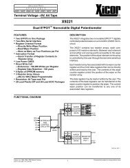
APPLICATION NOTES AND DEVELOPMENT SYSTEMA V A I L A B L EAN20 • AN42–48 • AN50–53 • AN73 • XK9241<strong>Terminal</strong> <strong>X9241</strong> Voltage ±5V, 64 Taps<strong>X9241</strong><strong>Quad</strong> E 2 POT <strong>Nonvolatile</strong> <strong>Digital</strong> <strong>Potentiometer</strong>FEATURES• Four E 2 POTs in One Package• Two-Wire Serial Interface• Register Oriented Format—Directly Write Wiper Position—Read Wiper Position—Store as Many as Four Positions per Pot• Instruction Format—Quick Transfer of Register Contents toResistor Array—Cascade Resistor Arrays• Low Power CMOS• Direct Write Cell—Endurance - 100,000 Data Changes per Register—Register Data Retention - 100 years• 16 Bytes of E 2 PROM memory• 3 Resistor Array Values—2KΩ to 50KΩ Mask Programmable—Cascadable For Values of 500Ω to 200KΩ• Resolution: 64 Taps each Pot• 20-Lead Plastic DIP, 20-Lead TSSOP and20-Lead SOIC PackagesDESCRIPTIONThe <strong>X9241</strong> integrates four nonvolatile E 2 POT digitallycontrolled potentiometers on a monolithic CMOS microcircuit.The <strong>X9241</strong> contains four resistor arrays, each composedof 63 resistive elements. Between each elementand at either end are tap points accessible to the wiperelements. The position of the wiper element on the arrayis controlled by the user through the two-wire serial businterface.Each resistor array has associated with it a wiper counterregister and four 8-bit data registers that can be directlywritten and read by the user. The contents of the wipercounter register control the position of the wiper on theresistor array.The data register may be read or written by the user. Thecontents of the data registers can be transferred to thewiper counter register to position the wiper. The currentwiper position can be transferred to any one of itsassociated data registers.The arrays may be cascaded to form resistive elementswith 127, 190 or 253 taps.FUNCTIONAL DIAGRAMSCLSDAA0A1A2A3INTERFACEANDCONTROLCIRCUITRYDATA8R0R2R0R2R1R3R1R3WIPERCOUNTERREGISTER(WCR)WIPERCOUNTERREGISTER(WCR)RESISTORARRAYPOT 1VH0VL0VW0VH1VL1VW1R0R2R0R2R1R3R1R3WIPERCOUNTERREGISTER(WCR)WIPERCOUNTERREGISTER(WCR)RESISTORARRAYPOT 2RESISTORARRAYPOT 3VH2VL2VW2VH3VL3VW33864 ILL F07.1© Xicor, Inc. 1994, 1995, 1996 Patents Pending Characteristics subject to change without notice3864-2.7 7/1/96 T0/C3/D3 NS1
<strong>X9241</strong>Figure 4. Three-Byte Command SequenceSCLSDASTART0 1 0 1 A3 A2 A1 A0 ACKI3 I2 I1 I0 P1 P0 R1 R0 ACKCM DW D5 D4 D3 D2 D1 D0ACKSTOP3864 ILL F11Figure 5. Increment/Decrement Command SequenceSCLSDAXX0 1 0 1 A3 A2 A1 A0 I3 I2 I1 I0 P1 P0 STAACKR1 R0 ACKRTINC1INC2INCnDEC1DECnSTOP3864 FHD F12Figure 6. Increment/Decrement Timing LimitsINC/DECCMDISSUEDt CLWVSCLSDAV WVOLTAGE OUT3864 ILL F135
<strong>X9241</strong>Table 1. Instruction SetInstruction FormatInstruction I 3 I 2 I 1 I 0 P 1 P 0 R 1 R o OperationRead WCR 1 0 0 1 1/0(7) 1/0 N/A(8) N/A Read the contents of the Wiper CounterRegister pointed to by P 1 –P 0Write WCR 1 0 1 0 1/0 1/0 N/A N/A Write new value to the Wiper CounterRegister pointed to by P 1 –P 0Read Data 1 0 1 1 1/0 1/0 1/0 1/0 Read the contents of the RegisterRegister pointed to by P 1 –P 0 and R 1 –R 0Write Data 1 1 0 0 1/0 1/0 1/0 1/0 Write new value to the RegisterRegister pointed to by P 1 –P 0 and R 1 –R 0XFR Data Reg- 1 1 0 1 1/0 1/0 1/0 1/0 Transfer the contents of the Registerister to WCR pointed to by P 1 –P 0 and R 1 –R 0to its associated WCRXFR WCR to 1 1 1 0 1/0 1/0 1/0 1/0 Transfer the contents of the WCRData Registerpointed to by P 1 –P 0 to the Registerpointed to by R 1 –R 0Global XFR Data 0 0 0 1 N/A N/A 1/0 1/0 Transfer the contents of all four DataRegister to WCRRegisters pointed to by R 1 –R 0 to theirrespective WCRGlobal XFR WCR 1 0 0 0 N/A N/A 1/0 1/0 Transfer the contents of all WCRsto Data Registerto their respective data Registerspointed to by R 1 –R 0Increment/Decre- 0 0 1 0 1/0 1/0 N/A N/A Enable Increment/decrement of thement Wiper WCR pointed to by P 1 –P 03864 PGM T02.1Notes: (7) 1/0 = data is one or zero(8) N/A = Not applicable or don't care; that is, a data register is not involved in the operation and need not be addressed (typical)Figure 7. Acknowledge Response from ReceiverSCL FROMMASTER1 8 9DATAOUTPUTFROMTRANSMITTERDATAOUTPUTFROMRECEIVERSTARTACKNOWLEDGE3864 ILL F146
<strong>X9241</strong>DETAILED OPERATIONAll four E2POT potentiometers share the serial interfaceand share a common architecture. Each potentiometeris comprised of a resistor array, a wiper counter registerand four data registers. A detailed discussion of theregister organization and array operation follows.Wiper Counter RegisterThe <strong>X9241</strong> contains four wiper counter registers (WCR),one for each E2POT potentiometer. The WCR can beenvisioned as a 6-bit parallel and serial load counter withits outputs decoded to select one of sixty-four switchesalong its resistor array. The contents of the WCR can bealtered in four ways: it may be written directly by the hostvia the Write WCR instruction (serial load); it may bewritten indirectly by transferring the contents of one offour associated data registers via the XFR Data Registerinstruction (parallel load); it can be modified one step ata time by the Increment/ Decrement instruction; finally,it is loaded with the contents of its data register zero (R0)upon power-up.Figure 8. Detailed <strong>Potentiometer</strong> Block DiagramThe WCR is a volatile register; that is, its contents arelost when the <strong>X9241</strong> is powered-down. Although theregister is automatically loaded with the value in R0upon power-up, it should be noted this may be differentfrom the value present at power-down.Data RegistersEach potentiometer has four nonvolatile data registers.These can be read or written directly by the host anddata can be transferred between any of the four dataregisters and the WCR. It should be noted all operationschanging data in one of these registers is a nonvolatileoperation and will take a maximum of 10ms.If the application does not require storage of multiplesettings for the potentiometer, these registers can beused as regular memory locations that could possiblystore system parameters or user preference data.SERIAL DATA PATHFROM INTERFACECIRCUITRYSERIALBUSINPUTV HREGISTER 0 REGISTER 18 6REGISTER 2 REGISTER 3PARALLELBUSINPUTWIPERCOUNTERREGISTERCOUNTERIF WCR = 00[H] THEN VW = VLIF WCR = 3F[H] THEN VW = VH2UP/DNMODIFIED SCLUP/DNCLKINC/DECLOGICDECODEV LDWCASCADECONTROLLOGICCMV W3864 ILL F157
<strong>X9241</strong>Cascade ModeThe <strong>X9241</strong> provides a mechanism for cascading thearrays. That is, the sixty-three resistor elements of onearray may be cascaded (linked) with the resistor elementsof an adjacent array.Cascade Control BitsThe data byte, for the three-byte commands, contains 6bits (LSBs) for defining the wiper position plus two highorder bits, CM (Cascade Mode) and DW (Disable Wiper).The state of CM enables or disables (normal operation)cascade mode. When the CM bit of the WCR is set to “0”the potentiometer is in the normal operation mode.When the CM bit of the WCR is set to “1” the potentiometeris cascaded with its adjacent higher order potentiometer.For example; if bit 7 of WCR2 is set to “1”, pot 2 will becascaded to pot 3.The state of DW enables or disables the wiper. When theDW bit of the WCR is set to “0” the wiper is enabled;when set to “1” the wiper is disabled. If the wiper isdisabled, the wiper terminal will be electrically isolatedand float.When operating in cascade mode VH, VL and the wiperterminals of the cascaded arrays must be electricallyconnected externally. All but one of the wipers must bedisabled. The user can alter the wiper position by writingdirectly to the WCR or indirectly by transferring thecontents of the data registers to the WCR or by using theIncrement/Decrement command.When using the Increment/Decrement command thewiper position will automatically transition betweenarrays. The current position of the wiper can be determinedby reading the WCR registers; if the DW bit is “0”,the wiper in that array is active. If the current wiperposition is to be maintained, a global XFR WCR to DataRegister command must be issued before power-down.Figure 9. Cascading ArraysPOT 0WCR0VL0VH0VW0POT 1WCR1VL1VH1VW1POT 2WCR2VL2VH2VW2=EXTERNAL CONNECTIONPOT 3WCR3VL3VH3VW33864 ILL F16.18
<strong>X9241</strong>ABSOLUTE MAXIMUM RATINGS*Temperature under Bias .................. –65°C to +135°CStorage Temperature ....................... –65°C to +150°CVoltage on SCK, SCL or any Address Inputwith Respect to V SS ................................... –1V to +7VVoltage on any V H or V L Referenced to V SS ......... ±8V∆V = |V H –V L | ......................................................... 16VLead Temperature (Soldering, 10 seconds)...... 300°CRECOMMENDED OPERATING CONDITIONSTemperature Min. Max.Commercial 0°C +70°CIndustrial –40°C +85°CMilitary –55°C +125°C3864 PGM T033864 PGM T06.3Notes: (1) Absolute Linearity is utilized to determine actual wiper voltage versus expected voltage as determined by wiperposition when used as a potentiometer.(2) Relative Linearity is utilized to determine the actual change in voltage between two successive tap positions when used as apotentiometer. It is a measure of the error in step size.(3) MI = RTOT/63 or (V H – V L )/63, single pot(4) Max. = all four arrays cascaded together, Typical = individual array resolutions.9*COMMENTStresses above those listed under “Absolute MaximumRatings” may cause permanent damage to the device.This is a stress rating only and the functional operation ofthe device at these or any other conditions above thoseindicated in the operational sections of this specification isnot implied. Exposure to absolute maximum rating conditionsfor extended periods may affect device reliability.Supply VoltageLimits<strong>X9241</strong> 5V ±10%ANALOG CHARACTERISTICS (Over recommended operating conditions unless otherwise stated.)LimitsSymbol Parameter Min. Typ. Max. Units Test ConditionsR TOTAL End to End Resistance –20 +20 %Power Rating 50 mW 25°C, each potI W Wiper Current –1 +1 mAR W Wiper Resistance 40 100 Ω Wiper Current = ± 1mAV TERM Voltage on any V H or –5 +5 Vor V L PinNoise ≤120 dB/ Ref: 1VResolution (4) 1.6 0.4 %3864 PGM T04.1Absolute Linearity (1) –1 +1 MI(3) V w(n)(actual) – V w(n)(expected)Relative Linearity (2) –0.2 +0.2 MI(3) V w(n + 1) – [V w(n) + MI ]Temperature Coefficient ±300 ppm/°C3864 PGM T05.2D.C. OPERATING CHARACTERISTICS (Over recommended operating conditions unless otherwise stated.)LimitsSymbol Parameter Min. Typ. Max. Units Test Conditionsl CC Supply Current (Active) 3 mA f SCL = 100KHz, SDA = Open,Other Inputs = V SSI SB V CC Current (Standby) 200 500 µA SCL=SDA=V CC , Addr. = V SSI LI Input Leakage Current 10 µA V IN = V SS to V CCI LO Output Leakage Current 10 µA V OUT = V SS to V CCV IH Input HIGH Voltage 2 V CC + 1 VV IL Input LOW Voltage –1 0.8 VV OL Output LOW Voltage 0.4 V I OL = 3mA
<strong>X9241</strong>ENDURANCE AND DATA RETENTIONParameter Min. UnitsMinimum Endurance 100,000 Data Changes per RegisterData Retention 100 Years3864 PGM T07.2CAPACITANCESymbol Parameter Max. Units Test ConditionsC (5) I/O Input/Output Capacitance (SDA) 8 pF V I/O = 0VC IN(5) Input Capacitance (A0, A1, A2, A3 and SCL) 6 pF V IN = 0V3864 PGM T08POWER-UP TIMINGSymbol Parameter Max. Unitst PUR(6) Power-up to Initiation of Read Operation 1 mst (6) PUW Power-up to Initiation of Write Operation 5 ms3864 PGM T09A.C. CONDITIONS OF TESTInput Pulse Levels V CC x 0.1 to V CC x 0.9Input Rise andFall Times10nsInput and OutputTiming Levels V CC x 0.53864 PGM T10Notes: (5) This parameter is periodically sampled and not 100%tested.(6) t PUR and t PUW are the delays required from the timeVCC is stable until the specified operation can beinitiated. These parameters are periodically sampledand not 100% tested.SYMBOL TABLEEQUIVALENT A.C. TEST CIRCUITSDA OUTPUTGuidelines for CalculatingTypical Values of Bus Pull-Up Resistors5V1533Ω100pF3864 ILL F02.1WAVEFORM INPUTS OUTPUTS120Must besteadyMay changefrom LOW to HIGHMay changefrom HIGH to LOWDon’t Care:ChangesAllowedN/AWill besteadyWill changefrom LOWto HIGHWill changefrom HIGHto LOWChanging:State NotKnownCenter Lineis HighImpedanceRESISTANCE (KΩ)100806040R MIN= IOL MINtR MAX= RCBUSMAX.RESISTANCEV CC MAX =1.8KΩ20MIN.RESISTANCE00 20 40 60 80 100 120BUS CAPACITANCE (pF)3864 ILL F1710
<strong>X9241</strong>A.C. CHARACTERISTICS (Over recommended operating conditions unless otherwise stated)LimitsReferenceSymbol Parameter Min. Max. Units Figuref SCL SCL Clock Frequency 0 100 KHz 10t LOW Clock LOW Period 4700 ns 10t HIGH Clock HIGH Period 4000 ns 10t R SCL and SDA Rise Time 1000 ns 10t F SCL and SDA Fall Time 300 ns 10Ti Noise Suppression Time Constant 100 ns 10(Glitch Filter)t SU:STA Start Condition Setup Time (for a Repeated 4700 ns 10 & 12Start Condition)t HD:STA Start Condition Hold Time 4000 ns 10 & 12t SU:DAT Data in Setup Time 250 ns 10t HD:DAT Data in Hold Time 0 ns 10t AA SCL LOW to SDA Data Out Valid 300 3500 ns 11t DH Data Out Hold Time 300 ns 11t SU:STO Stop Condition Setup Time 4700 ns 10 & 12t BUF Bus Free Time Prior to New Transmission 4700 ns 10t WR Write Cycle Time (<strong>Nonvolatile</strong> Write Operation) 10 ms 13t STPWV Wiper Response Time From Stop Generation 500 µs 13t CLWV Wiper Response From SCL LOW 1000 µs 6t R V CC V CC Power-up Rate 0.2 50 mV/µs3864 PGM T11.3Figure 10. Input Bus Timingt HIGHt LOW t F t Rt SU:STOSCLt SU:STA t HD:STA t HD:DAT t SU:DATSDA(DATA IN)t BUF3864 ILL F0311
<strong>X9241</strong>Figure 11. Output Bus TimingSCLt AAt DHSDA SDA OUT (ACK) SDA OUT SDA OUT3864 ILL F053864 ILL F04Figure 12. Start Stop TimingSTART CONDITIONSTOP CONDITIONSCLt SU:STAt HD:STAt SU:STOSDADATA INFigure 13. Write Cycle and Wiper Response TimingSCLSDACLOCK 8CLOCK 9SDA INACKSTOPt WRSTARTt STPWVWIPEROUTPUT3864 ILL F0612
<strong>X9241</strong>PACKAGING INFORMATION20-LEAD PLASTIC DUAL IN-LINE PACKAGE TYPE P1.060 (26.92)0.980 (24.89)0.280 (7.11)0.240 (6.096)PIN 1 INDEXPIN 10.900 (23.66)REF.—0.005 (0.127)SEATINGPLANE(3.81) 0.150(2.92) 0.11500.195 (4.95)0.115 (2.92)––0.015 (0.38)0.10 (BSC)(2.54)0.070 (1.778)0.045 (1.143)0.022 (0.559)0.014 (0.356)0.300(7.62) (BSC)0.014 (0.356)0.008 (0.2032)0°15°NOTE:1. ALL DIMENSIONS IN INCHES (IN PARENTHESES IN MILLIMETERS)2. PACKAGE DIMENSIONS EXCLUDE MOLDING FLASH3926 FHD F18.113
<strong>X9241</strong>PACKAGING INFORMATION20-LEAD PLASTIC SMALL OUTLINE GULL WING PACKAGE TYPE S0.290 (7.37)0.299 (7.60)0.393 (10.00)0.420 (10.65)PIN 1 INDEXPIN 10.014 (0.35)0.020 (0.50)0.496 (12.60)0.508 (12.90)(4X) 7°0.092 (2.35)0.105 (2.65)0.050 (1.27)0.003 (0.10)0.012 (0.30)0.050" Typical0.010 (0.25)0.020 (0.50)X 45°0° – 8°0.007 (0.18)0.011 (0.28)0.420"0.050"Typical0.015 (0.40)0.050 (1.27)FOOTPRINT0.030" Typical20 PlacesNOTE: ALL DIMENSIONS IN INCHES (IN PARENTHESES IN MILLIMETERS)3926 FHD F2314
<strong>X9241</strong>PACKAGING INFORMATION20-LEAD PLASTIC, TSSOP PACKAGE TYPE V.025 (.65) BSC.169 (4.3).177 (4.5).252 (6.4) BSC.252 (6.4).300 (6.6).047 (1.20).0075 (.19).0118 (.30).002 (.05).006 (.15)0° – 8°.019 (.50).029 (.75)Detail A (20X).010 (.25)Gage PlaneSeating Plane.031 (.80).041 (1.05)See Detail “A”NOTE: ALL DIMENSIONS IN INCHES (IN PARENTHESES IN MILLIMETERS)3926 FHD F4515
<strong>X9241</strong>ORDERING INFORMATION<strong>X9241</strong> Y P T VDeviceV CC LimitsBlank = 5V ±10%Temperature RangeBlank = Commercial = 0°C to +70°CI = Industrial = –40°C to +85°CM = Military = –55°C to +125°CPackageP = 20-Lead Plastic DIPS = 20-Lead SOICV = 20-Lead TSSOP<strong>Potentiometer</strong> OrganizationPot 0 Pot 1 Pot 2 Pot 3Y = 2K 2K 2K 2KW = 10K 10K 10K 10KU = 50K 50K 50K 50KM = 2K 10K 10K 50KLIMITED WARRANTYDevices sold by Xicor, Inc. are covered by the warranty and patent indemnification provisions appearing in its Terms of Sale only. Xicor, Inc. makes no warranty,express, statutory, implied, or by description regarding the information set forth herein or regarding the freedom of the described devices from patent infringement.Xicor, Inc. makes no warranty of merchantability or fitness for any purpose. Xicor, Inc. reserves the right to discontinue production and change specifications andprices at any time and without notice.Xicor, Inc. assumes no responsibility for the use of any circuitry other than circuitry embodied in a Xicor, Inc. product. No other circuits, patents, licenses areimplied.U.S. PATENTSXicor products are covered by one or more of the following U.S. Patents: 4,263,664; 4,274,012; 4,300,212; 4,314,265; 4,326,134; 4,393,481; 4,404,475;4,450,402; 4,486,769; 4,488,060; 4,520,461; 4,533,846; 4,599,706; 4,617,652; 4,668,932; 4,752,912; 4,829, 482; 4,874, 967; 4,883, 976. Foreign patents andadditional patents pending.LIFE RELATED POLICYIn situations where semiconductor component failure may endanger life, system designers using this product should design the system with appropriate errordetection and correction, redundancy and back-up features to prevent such an occurrence.Xicor's products are not authorized for use in critical components in life support devices or systems.1. Life support devices or systems are devices or systems which, (a) are intended for surgical implant into the body, or (b) support or sustain life, and whosefailure to perform, when properly used in accordance with instructions for use provided in the labeling, can be reasonably expected to result in a significantinjury to the user.2. A critical component is any component of a life support device or system whose failure to perform can be reasonably expected to cause the failure of the lifesupport device or system, or to affect its safety or effectiveness.16
<strong>X9241</strong>U.S. SALES OFFICESCorporate OfficeXicor Inc.1511 Buckeye DriveMilpitas, CA 95035Phone: 408/432-8888Fax: 408/432-0640E-mail: info@smtpgate.xicor.comNortheast RegionXicor Inc.1344 Main StreetWaltham, MA 02154Phone: 617/899-5510Fax: 617/899-6808E-mail: xicor-ne@smtpgate.xicor.comSoutheast RegionXicor Inc.100 E. Sybelia Ave.Suite 355Maitland, FL 32751Phone: 407/740-8282Fax: 407/740-8602E-mail: xicor-se@smtpgate.xicor.comMid-Atlantic RegionXicor Inc.50 North StreetDanbury, CT 06810Phone: 203/743-1701Fax: 203/794-9501E-mail: xicor-ma@smtpgate.xicor.comNorth Central RegionXicor Inc.810 South Bartlett RoadSuite 103Streamwood, IL 60107Phone: 708/372-3200Fax: 708/372-3210E-mail: xicor-nc@smtpgate.xicor.comSouth Central RegionXicor Inc.11884 Greenville Ave.Suite 102Dallas, TX 75243Phone: 214/669-2022Fax: 214/644-5835E-mail: xicor-sc@smtpgate.xicor.comSouthwest RegionXicor Inc.4100 Newport Place DriveSuite 710Newport Beach, CA 92660Phone: 714/752-8700Fax: 714/752-8634E-mail: xicor-sw@smtpgate.xicor.comNorthwest RegionXicor Inc.2700 Augustine DriveSuite 219Santa Clara, CA 95054Phone: 408/292-2011Fax: 408/980-9478E-mail: xicor-nw@smtpgate.xicor.comINTERNATIONAL SALES OFFICESEUROPENorthern EuropeXicor Ltd.Grant Thornton HouseWitan WayWitneyOxford OX8 6FEUKPhone: (44) 1933.700544Fax: (44) 1933.700533E-mail: xicor-uk@smtpgate.xicor.comCentral EuropeXicor GmbHTechnopark NeukeferlohBretonischer Ring 1585630 Grasbrunn bei MuenchenGermanyPhone: (49) 8946.10080Fax: (49) 8946.05472E-mail: xicor-gm@smtpgate.xicor.comASIA/PACIFICJapanXicor Japan K.K.Suzuki Building, 4th Floor1-6-8 Shinjuku, Shinjuku-kuTokyo 160, JapanPhone: (81) 3322.52004Fax: (81) 3322.52319E-mail: xicor-jp@smtpgate.xicor.comMainland ChinaTaiwan/Hong KongXicor Inc.4100 Newport Place DriveSuite 710Newport Beach, CA 92660Phone: 714/752-8700Fax: 714/752-8634E-mail: xicor-sw@smtpgate.xicor.comSingapore/Malaysia/IndiaXicor Inc.2700 Augustine DriveSuite 219Santa Clara, CA 95054Phone: 408/292-2011Fax: 408/980-9478E-mail: xicor-nw@smtpgate.xicor.comKoreaXicor Korea27th Fl., Korea World Trade Ctr.159, Samsung-dongKangnam KuSeoul 135-729KoreaPhone: (82) 2551.2750Fax: (82) 2551.2710E-mail: xicor-ka@smtpgate.xicor.com( ) = Country CodeXicor product information is available at:http://www.xicor.comXicor, Inc., Marketing Dept. 1511 Buckeye Drive, Milpitas, California 95035-7493 TEL 408/432-8888 FAX 408/432-0640 Rev. 4 3/96 Stock# XX-X-XXXX17