- Page 1 and 2: Z8018xFamily MPUUser ManualUM005001
- Page 3 and 4: Z8018x FamilyMPU User ManualiiiMANU
- Page 5 and 6: Z8018x FamilyMPU User ManualvTable
- Page 7 and 8: Z8018x FamilyMPU User ManualviiFlag
- Page 9 and 10: Z8018x FamilyMPU User ManualxFigure
- Page 11 and 12: Z8018x FamilyMPU User ManualxiiSoft
- Page 13 and 14: Z8018x FamilyMPU User ManualxvTable
- Page 15 and 16: Z8018x FamilyMPU User ManualxvUM005
- Page 17 and 18: Z8018x FamilyM PU User M anual2on-c
- Page 19 and 20: Z8018x FamilyM PU User M anual4UM00
- Page 21 and 22: Z8018x FamilyM PU User M anual6XTAL
- Page 23 and 24: Z8018x FamilyM PU User M anual8D0-D
- Page 25 and 26: Z8018x FamilyM PU User M anual10RTS
- Page 27 and 28: Z8018x FamilyM PU User M anual12Tab
- Page 29 and 30: Z8018x FamilyM PU User M anual14Cen
- Page 31 and 32: Z8018x FamilyM PU User M anual16T1
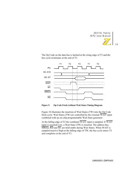
- Page 33: Z8018x FamilyM PU User M anual18Not
- Page 37 and 38: Z8018x FamilyM PU User M anual22Phi
- Page 39 and 40: Z8018x FamilyM PU User M anual241st
- Page 41 and 42: Z8018x FamilyM PU User M anual26Whe
- Page 43 and 44: Z8018x FamilyM PU User M anual28ext
- Page 45 and 46: Z8018x FamilyM PU User M anual30ins
- Page 47 and 48: Z8018x FamilyM PU User M anual32•
- Page 49 and 50: Z8018x FamilyM PU User M anual34•
- Page 51 and 52: Z8018x FamilyM PU User M anual36Low
- Page 53 and 54: Z8018x FamilyM PU User M anual381.
- Page 55 and 56: Z8018x FamilyM PU User M anual40If
- Page 57 and 58: Z8018x FamilyM PU User M anual42To
- Page 59 and 60: Z8018x FamilyM PU User M anual44add
- Page 61 and 62: Z8018x FamilyM PU User M anual46Tab
- Page 63 and 64: Z8018x FamilyM PU User M anual48Tab
- Page 65 and 66: Z8018x FamilyM PU User M anual50Tab
- Page 67 and 68: Z8018x FamilyM PU User M anual52Clo
- Page 69 and 70: Z8018x FamilyM PU User M anual54Bit
- Page 71 and 72: Z8018x FamilyM PU User M anual56FFF
- Page 73 and 74: Z8018x FamilyM PU User M anual58•
- Page 75 and 76: Z8018x FamilyM PU User M anual60MMU
- Page 77 and 78: Z8018x FamilyM PU User M anual62MMU
- Page 79 and 80: Z8018x FamilyM PU User M anual64MMU
- Page 81 and 82: Z8018x FamilyM PU User M anual66Fun
- Page 83 and 84: Z8018x FamilyM PU User M anual68INT
- Page 85 and 86:
Z8018x FamilyM PU User M anual70Tab
- Page 87 and 88:
Z8018x FamilyM PU User M anual72Phi
- Page 89 and 90:
Z8018x FamilyM PU User M anual74NMI
- Page 91 and 92:
Z8018x FamilyM PU User M anual76Las
- Page 93 and 94:
Z8018x FamilyM PU User M anual78Las
- Page 95 and 96:
Z8018x FamilyM PU User M anual80Las
- Page 97 and 98:
Z8018x FamilyM PU User M anual82ind
- Page 99 and 100:
Z8018x FamilyM PU User M anual84Ret
- Page 101 and 102:
Z8018x FamilyM PU User M anual86Las
- Page 103 and 104:
Z8018x FamilyM PU User M anual88Ref
- Page 105 and 106:
Z8018x FamilyM PU User M anual903.
- Page 107 and 108:
Z8018x FamilyM PU User M anual92Cha
- Page 109 and 110:
Z8018x FamilyM PU User M anual94DMA
- Page 111 and 112:
Z8018x FamilyM PU User M anual96Bit
- Page 113 and 114:
Z8018x FamilyM PU User M anual98Bit
- Page 115 and 116:
Z8018x FamilyM PU User M anual100Ta
- Page 117 and 118:
Z8018x FamilyM PU User M anual102Ta
- Page 119 and 120:
Z8018x FamilyM PU User M anual104Bi
- Page 121 and 122:
Z8018x FamilyM PU User M anual106DM
- Page 123 and 124:
Z8018x FamilyM PU User M anual108ri
- Page 125 and 126:
Z8018x FamilyM PU User M anual110DR
- Page 127 and 128:
Z8018x FamilyM PU User M anual1124.
- Page 129 and 130:
Z8018x FamilyM PU User M anual114DM
- Page 131 and 132:
Z8018x FamilyM PU User M anual116Th
- Page 133 and 134:
Z8018x FamilyM PU User M anual118Wh
- Page 135 and 136:
Z8018x FamilyM PU User M anual1200,
- Page 137 and 138:
Z8018x FamilyM PU User M anual122Bi
- Page 139 and 140:
Z8018x FamilyM PU User M anual124Bi
- Page 141 and 142:
Z8018x FamilyM PU User M anual126Bi
- Page 143 and 144:
Z8018x FamilyM PU User M anual128AS
- Page 145 and 146:
Z8018x FamilyM PU User M anual130Bi
- Page 147 and 148:
Z8018x FamilyM PU User M anual132AS
- Page 149 and 150:
Z8018x FamilyM PU User M anual134pi
- Page 151 and 152:
Z8018x FamilyM PU User M anual136Bi
- Page 153 and 154:
Z8018x FamilyM PU User M anual138AS
- Page 155 and 156:
Z8018x FamilyM PU User M anual140I/
- Page 157 and 158:
Z8018x FamilyM PU User M anual142Ta
- Page 159 and 160:
Z8018x FamilyM PU User M anual144al
- Page 161 and 162:
Z8018x FamilyM PU User M anual146ca
- Page 163 and 164:
Z8018x FamilyM PU User M anual148Bi
- Page 165 and 166:
Z8018x FamilyM PU User M anual150CS
- Page 167 and 168:
Z8018x FamilyM PU User M anual152c.
- Page 169 and 170:
Z8018x FamilyM PU User M anual154CK
- Page 171 and 172:
Z8018x FamilyM PU User M anual156CK
- Page 173 and 174:
Z8018x FamilyM PU User M anual158re
- Page 175 and 176:
Z8018x FamilyM PU User M anual160Ti
- Page 177 and 178:
Z8018x FamilyM PU User M anual162Bi
- Page 179 and 180:
Z8018x FamilyM PU User M anual164Ph
- Page 181 and 182:
Z8018x FamilyM PU User M anual166Th
- Page 183 and 184:
Z8018x FamilyM PU User M anual168SL
- Page 185 and 186:
Z8018x FamilyM PU User M anual170CL
- Page 187 and 188:
Z8018x FamilyM PU User M anual172Mi
- Page 189 and 190:
Z8018x FamilyM PU User M anual174ML
- Page 191 and 192:
Z8018x FamilyM PU User M anual176Fi
- Page 193 and 194:
Z8018x FamilyM PU User M anual178St
- Page 195 and 196:
Z8018x FamilyM PU User M anual180Ad
- Page 197 and 198:
Z8018x FamilyM PU User M anual182In
- Page 199 and 200:
Z8018x FamilyM PU User M anual184IO
- Page 201 and 202:
Z8018x FamilyMPU User Manual186Z801
- Page 203 and 204:
Z8018x FamilyMPU User Manual188Tabl
- Page 205 and 206:
Z8018x FamilyMPU User Manual190Tabl
- Page 207 and 208:
Z8018x FamilyMPU User Manual192UM00
- Page 209 and 210:
Z8018x FamilyMPU User Manual194No.S
- Page 211 and 212:
Z8018x FamilyMPU User Manual196Tabl
- Page 213 and 214:
Z8018x FamilyMPU User Manual197Timi
- Page 215 and 216:
Z8018x FamilyMPU User Manual199I/O
- Page 217 and 218:
Z8018x FamilyMPU User Manual201T 1
- Page 219 and 220:
Z8018x FamilyMPU User Manual203SLP
- Page 221 and 222:
Z8018x FamilyMPU User Manual205STAN
- Page 223 and 224:
Z8018x FamilyMPU User Manual207Inst
- Page 225 and 226:
Z8018x FamilyMPU User Manual209REST
- Page 227 and 228:
Z8018x FamilyMPU User Manual211DATA
- Page 229 and 230:
Z8018x FamilyMPU User Manual213Tabl
- Page 231 and 232:
Z8018x FamilyMPU User Manual215Tabl
- Page 233 and 234:
Z8018x FamilyMPU User Manual217Tabl
- Page 235 and 236:
Z8018x FamilyMPU User Manual219Tabl
- Page 237 and 238:
Z8018x FamilyMPU User Manual221Tabl
- Page 239 and 240:
Z8018x FamilyMPU User Manual223Tabl
- Page 241 and 242:
Z8018x FamilyMPU User Manual225Tabl
- Page 243 and 244:
Z8018x FamilyMPU User Manual227Tabl
- Page 245 and 246:
Z8018x FamilyMPU User Manual229PROG
- Page 247 and 248:
Z8018x FamilyMPU User Manual231Tabl
- Page 249 and 250:
Z8018x FamilyMPU User Manual233Tabl
- Page 251 and 252:
Z8018x FamilyMPU User Manual235Spec
- Page 253 and 254:
Z8018x FamilyMPU User Manual237Inst
- Page 255 and 256:
Z8018x FamilyMPU User Manual239MNEM
- Page 257 and 258:
Z8018x FamilyMPU User Manual241MNEM
- Page 259 and 260:
Z8018x FamilyMPU User Manual243MNEM
- Page 261 and 262:
Z8018x FamilyMPU User Manual245MNEM
- Page 263 and 264:
Z8018x FamilyMPU User Manual247Op C
- Page 265 and 266:
Z8018x FamilyMPU User Manual249Tabl
- Page 267 and 268:
Z8018x FamilyMPU User Manual251Bus
- Page 269 and 270:
Z8018x FamilyMPU User Manual253Tabl
- Page 271 and 272:
Z8018x FamilyMPU User Manual255Tabl
- Page 273 and 274:
Z8018x FamilyMPU User Manual257Tabl
- Page 275 and 276:
Z8018x FamilyMPU User Manual259Tabl
- Page 277 and 278:
Z8018x FamilyMPU User Manual261Tabl
- Page 279 and 280:
Z8018x FamilyMPU User Manual263Tabl
- Page 281 and 282:
Z8018x FamilyMPU User Manual265Tabl
- Page 283 and 284:
Z8018x FamilyMPU User Manual267Tabl
- Page 285 and 286:
Z8018x FamilyMPU User Manual269Tabl
- Page 287 and 288:
Z8018x FamilyMPU User Manual271Tabl
- Page 289 and 290:
Z8018x FamilyMPU User Manual273Tabl
- Page 291 and 292:
Z8018x FamilyMPU User Manual275Tabl
- Page 293 and 294:
Z8018x FamilyMPU User Manual277Tabl
- Page 295 and 296:
Z8018x FamilyMPU User Manual279INTE
- Page 297 and 298:
Z8018x FamilyMPU User Manual281Oper
- Page 299 and 300:
Z8018x FamilyMPU User Manual283Note
- Page 301 and 302:
Z8018x FamilyMPU User Manual285- DR
- Page 303 and 304:
Z8018x FamilyMPU User Manual287Stat
- Page 305 and 306:
Z8018x FamilyMPU User Manual289Tabl
- Page 307 and 308:
Z8018x FamilyMPU User Manual291Tabl
- Page 309 and 310:
Z8018x FamilyMPU User Manual293I/O
- Page 311 and 312:
Z8018x FamilyMPU User Manual295Tabl
- Page 313 and 314:
Z8018x FamilyMPU User Manual297Tabl
- Page 315 and 316:
Z8018x FamilyMPU User Manual299Tabl
- Page 317 and 318:
Z8018x FamilyMPU User Manual301Tabl
- Page 319 and 320:
Z8018x FamilyMPU User Manual303ORDE
- Page 321 and 322:
Z8018x FamilyMPU User Manual305AAC
- Page 323 and 324:
Z8018x FamilyMPU User Manual307cles
- Page 325 and 326:
Z8018x FamilyMPU User Manual309CSI/