datasheet: pdf - Farnell
datasheet: pdf - Farnell
datasheet: pdf - Farnell

Create successful ePaper yourself
Turn your PDF publications into a flip-book with our unique Google optimized e-Paper software.
LMH1980SDTV Vertical Interval Timing Diagrams (NTSC, PAL, 480I, 576I)30010303FIGURE 3. NTSC Odd Field Vertical Interval30010304FIGURE 4. NTSC Even Field Vertical Intervalwww.national.com 4
EDTV Vertical Interval Timing Diagram (480P, 576P)LMH198030010305FIGURE 5. 480P Vertical IntervalHDTV Vertical Interval Timing Diagram (720P, 1080P)30010314FIGURE 6. 720P (1080P) Vertical Interval5 www.national.com
LMH1980HDTV Vertical Interval Timing Diagrams (1080I)30010306FIGURE 7. 1080I Field 1 Vertical Interval30010307FIGURE 8. 1080I Field 2 Vertical Intervalwww.national.com 6
SD/EDTV Horizontal Interval Timing DiagramLMH198030010308FIGURE 9. SD/EDTV Horizontal Interval with Bi-level SyncSDTV Horizontal Interval Timing CharacteristicsV CC = 3.3V , T A = 25°C, No Input Filter, PAL Video Input from Tek TG700 Generator with AVG7 SD video moduleSymbol Parameter Conditions Typ Unitstd CSOUTtd HSOUTtd BPOUTComposite Sync Output Propagation Delay from InputSync Reference (O H )Horizontal Sync Output Propagation Delay from InputSync Reference (O H )Burst/Back Porch Timing Output Propagation Delay fromInput Sync Trailing EdgeSee Figure 9 525See Figure 9 530See Figure 9 400 nsT HSOUT Horizontal Sync Output Pulse Width See Figure 9 2.5 µsT BPOUT Burst/Back Porch Timing Output Pulse Width See Figure 9 3.0 µsnsnsEDTV Horizontal Interval Timing CharacteristicsV CC = 3.3V , T A = 25°C, No Input Filter, 576P Video Input from Tek TG700 Generator with AVG7 SD moduleSymbol Parameter Conditions Typ Unitstd CSOUTtd HSOUTtd BPOUTComposite Sync Output Propagation Delay from InputSync Reference (O H )Horizontal Sync Output Propagation Delay from InputSync Reference (O H )Burst/Back Porch Timing Output Propagation Delay fromInput Sync Trailing EdgeSee Figure 9 170 nsSee Figure 9 175 nsSee Figure 9 485 nsT HSOUT Horizontal Sync Output Pulse Width See Figure 9 2.3 µsT BPOUT Burst/Back Porch Timing Output Pulse Width See Figure 9 350 ns7 www.national.com
LMH1980HDTV Horizontal Interval Timing Diagram30010309FIGURE 10. HDTV Horizontal Interval with Tri-level SyncHDTV Horizontal Interval Timing CharacteristicsV CC = 3.3V , T A = 25°C, No Input Filter, 1080I Video Input from Tek TG700 Generator with AWVG7 HD moduleSymbol Parameter Conditions Typ Unitstd CSOUTtd HSOUTtd BPOUTComposite Sync Output Propagation Delay from InputSync Leading EdgeHorizontal Sync Output Propagation Delay from InputSync Reference (O H )Burst/Back Porch Timing Output Propagation Delay fromInput Sync Trailing EdgeSee Figure 10 150 nsSee Figure 10 60 nsSee Figure 10 450T HSOUT Horizontal Sync Output Pulse Width See Figure 10 525 nsT BPOUT Burst/Back Porch Timing Output Pulse Width See Figure 10 350 nsnswww.national.com 8
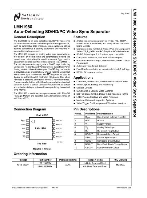
Application InformationGENERAL DESCRIPTIONThe LMH1980 is designed to extract the timing informationfrom various video formats with standard and non-standardvertical serration and output the syncs and relevant timingsignals in CMOS logic. Its advanced features and easy applicationmake it ideal for consumer, professional, and industrialvideo systems where sync timing needs to be extractedfrom SD, HD, and PC video signals. The device can operatefrom a supply voltage between 3.3V and 5V. The only requiredexternal components are bypass capacitors betweenthe V CC and GND pins, input coupling capacitor (C IN ) from thesignal source to the V IN pin, and a fixed-value 1% precisionresistor between the R EXT and GND pins. Refer to the testcircuit in Figure 2.R EXT ResistorThe precision external resistor (R EXT ) establishes the internalbias current and precise reference voltage for the LMH1980.For optimal performance, R EXT should be a 10 kΩ 1% precisionresistor with a low temperature coefficient to ensureproper operation over a wide temperature range. Using aR EXT resistor with less precision may result in reduced performance(like worse performance, increased propagationdelay variation, or reduced input sync amplitude range)against temperature, supply voltage, input signal, or part-topartvariations.Note: The R EXT resistor used with the LMH1980 serves a differentfunction than the “R SET resistor” used with other previoussync separators, like the LM1881. For the LM1881, theR SET value needed to be adjusted externally to support differentinput line rates. For the LMH1980, the R EXT value isfixed, and the device automatically detects the input line rateto support various video formats without electrical or physicalintervention.Automatic Format Detection and SwitchingAutomatic format detection eliminates the need for adjustingan external R SET resistor or programming via a microcontroller.The device outputs will respond correctly to a switchin video format after a sufficient start-up time has been satisfied,usually within 1 to 2 fields of video. Unlike other syncseparators, the LMH1980 does not require the power to becycled in order to produce correct outputs after a significantchange to the input signal. See the Start-up Time section formore details.Fixed-Level Sync SlicingThe LMH1980 uses fixed-level sync slicing for video inputswith an amplitude from 0.5V PP to 2V PP , which allows for propersync separation even for improperly terminated or attenuatedinput signals. The fixed-level sync slicing threshold isnominally 70 mV above the clamped sync tip. This means thatfor a minimum video input signal amplitude of 0.5V PP , theslicing level is near the mid-point of the sync pulse amplitude.This slicing level is independent of the input signal amplitude;therefore, for a 2V PP input, the slicing level occurs at 12% ofthe sync pulse amplitude.INPUT CONSIDERATIONSThe LMH1980 supports sync separation for analog CVBS, Y(luma) from Y/C and YP B P R , and G (sync on green) fromGBR/RGsB, as specified in the following video standards.• Composite Video (CVBS) and S-Video (Y/C):— SMPTE 170M (NTSC), ITU-R BT.470 (PAL)• Component Video (YP B P R /GBR):— SDTV: SMPTE 125M, SMPTE 267M, ITU-R BT.601(480I, 576I)— EDTV: ITU-R BT.1358 (480P, 576P)— HDTV: SMPTE 296M (720P), SMPTE 274M(1080I/P), SMPTE RP 211 (1080PsF)• PC Graphics (RGsB):— VESA Monitor Timing Standards and GuidelinesVersion 1.0, Revision 0.8• Non-Standard Video:— Composite NTSC & PAL (or Component 480I & 576I)without vertical serration & equalization pulses (i.e.:from logical OR-ing of H & V signals)Input TerminationThe video source should be load terminated with a 75Ω resistorto ensure correct video signal amplitude and minimizesignal distortion due to reflections. In extreme cases, theLMH1980 can handle non-terminated or double-terminatedinput conditions, assuming 1V PP signal amplitude for normallyterminated video.Input FilteringAn external filter is recommended if the video signal has largechroma amplitude that extends near the sync tip and/or hasconsiderable high-frequency noise, so they do not interferewith sync separation. A simple RC low-pass chroma filter witha series resistor (R 9 ) and a filter capacitor (C 2 ) to ground canbe used to sufficiently attenuate chroma such that minimumpeak of its amplitude is above the slicing level and also toimprove the overall signal-to-noise ratio. To achieve the desiredfilter cutoff frequency, it’s advised to vary C 2 and keepR 9 small (i.e.: 100Ω) to minimize sync tip clipping due to thevoltage drop across R 9 . Keep in mind that as the cutoff frequencydecreases, the LMH1980 output propagation delaysincrease, which could affect the timing relationship betweenthe sync and video signals.In applications where the chroma filter needs to be disabledwhen HD video is input, it is possible to use a transistor switch(Q1) controlled by the HD flag (pin 5) to open C 2 ’s connectionto ground as shown in Figure 11. When a HD tri-level syncinput signal is applied, HD will output logic low (following abrief delay for auto format detection) and Q1 will turn off todisable the chroma filter, which is intended for SD compositevideo only. When a SD bi-level sync signal (i.e.: NTSC/PAL)is applied, HD will output logic high and Q1 will turn on toenable the chroma filter.Important: If the filter cutoff frequency (f CO ) is set too low andHD video is applied, the filter can severely roll off and attenuatethe input's high-bandwidth tri-level sync pulses such thatthe LMH1980 cannot detect a valid HD input signal. If theLMH1980 cannot detect a valid HD input, then the HD flag willnever change from logic high to low and the switch-controlledfilter will never be disabled via Q1. In other words, f CO shouldnot be set too low that the filter impairs the LMH1980's abilityto detect a valid HD input. The values of R 9 and C 2 shown inFigure 11 give f CO =2.79 MHz (about -4 dB at 3.58 MHz NTSCsubcarrier frequency) without impairing HD video format detection.LMH19809 www.national.com
LMH198030010318FIGURE 11. External Switch-Controlled Chroma FilterIf a PC video input with bi-level sync is to be used, C 2 shouldbe removed to disable chroma filtering. This is necessary becauseHD will output logic high (like in the SD video inputcase) and enable the filter. A chroma filter could severelyband-limit a high-bandwidth PC video signal, which could rolloffand attenuate the sync pulses such that the LMH1980cannot detect a valid input signal.If some high-frequency noise filtering is needed for all videoinputs, a small capacitor (C 1 ) may be optionally used in parallelbut outside of the transistor switch. When Q1 is turnedon, then C 1 and C 2 will be connected in parallel (C 1 +C 2 )Input Coupling CapacitorThe input signal should be AC coupled to the V IN (pin 4) of theLMH1980 with a properly chosen coupling capacitor, C IN .The primary consideration in choosing C IN is whether theLMH1980 will interface with video sources using an AC-coupledoutput stage. If AC-coupled video sources are expectedin the end-application , then it’s recommended to choose asmall C IN value such as 0.01 µF to avoid missing sync outputpulses due to average picture level changes. It’s important tonote that video sources with an AC-coupled output will causevideo-dependent jitter at the HSync output of the sync separator.When only DC-coupled video sources are expected, alarger value for C IN may be used without concern for missingsync output pulses. A smaller C IN value can be used to increaserejection of source AC hum components and alsoreduce start-up time regardless of the video source's outputcoupling type.START-UP TIMEWhen there is a significant change to the video input signal,such as sudden signal switching in, signal attenuation (i.e.:load termination added via loop through) or signal gain (i.e.:load termination removed), the quiescent operation of theLMH1980 will be disrupted. During this dynamic input condition,the LMH1980 outputs may not be correct but will recoverto valid signals after a predictable start-up time, which consistsof an adjustable input settling time and a predetermined“sync lock time”.Input Settling Time and Coupling Capacitor SelectionFollowing a significant input condition, the negative sync tipof the AC-coupled signal settles to the input clamp voltage asthe coupling capacitor, C IN , recovers a quiescent DC voltagevia the dynamic clamp current through V IN . Because C IN determinesthe input settling time, its capacitance value is criticalwhen minimizing overall start-up time. A smaller C IN valueyields shorter settling time at the expense of increased linedroop voltage, whereas a larger one yields reduced line droopbut longer settling time. Settling time is proportional to thevalue of C IN , so doubling C IN will also double the settling time.Sync Lock TimeIn addition to settling time, the LMH1980 has a predeterminedsync lock time, T SYNC-LOCK , before the outputs are correct.Once the AC-coupled input has settled enough, the LMH1980needs time to detect the valid video signal and apply fixedlevelsync slicing before the output signals are correct.For practical values of C IN , T SYNC-LOCK is typically less than 1or 2 video fields in duration starting from the 1st valid VSyncoutput pulse to the valid HSync pulses beginning thereafter.VSync and HSync pulses are considered valid when theyalign correctly with the input's vertical and horizontal sync intervals.It is recommended for the outputs to be applied to the systemafter the start-up time is satisfied and outputs are valid. Forexample, the oscilloscope screenshot in Figure 12 shows atypical start-up time within 1 video field from when an NTSCsignal is just applied to when the LMH1980 outputs are valid.FIGURE 12. Typical Start-Up Time for NTSC Input toLMH1980 (C IN = 0.1 µF)30010317LOGIC OUTPUTSIn the absence of a video input signal, the LMH1980 outputsare logic high except for the odd/even field, which is undefinedand depends on its previous state, and the composite syncoutput.Horizontal Sync OutputHSOUT (pin 6) produces a negative-polarity horizontal syncsignal, or HSync, extracted from the input signal. For bi-leveland tri-level sync signals, HSync's negative-going leadingedge is derived from the input's sync reference, O H , with apropagation delay.Important: The HSync output has good performance on itsnegative-going leading edge, so it should be used as the referenceto a negative-edge triggered PLL input. If HSync isused as the reference to a positive-edge triggered PLL input,like in some FPGAs, the signal must be inverted first to producea positive-polarity HSync signal (i.e.: positive-goingleading edge) before the PLL input. HSync's trailing edgeshould not be used as the reference to a PLL because for aNTSC/PAL input, the input's half-width pulses (½T SYNC ) in thevertical interval cause the trailing edges of the HSync outputto occur earlier than for the normal-width sync pulses(T SYNC ). This bi-modal timing variation on HSync's trailingedge, as shown in Figure 13, could affect the performance ofthe PLL. The bi-modal trailing edge timing also occurs on theCSync output as well.www.national.com 10
during an odd field (field 1) and logic low during an even field(field 2). The odd/even output edge transitions align withVSync's leading edge to designate the start of odd and evenfields. For progressive (non-interlaced) video formats, theoutput is held constantly at logic high.LMH198030010313FIGURE 13. Bi-modal Timing on HSync's Trailing Edgefor Half-Width Pulses for NTSCVertical Sync OutputVSOUT (pin 7) produces a negative-polarity vertical sync signal,or VSync. VSync's negative-going leading edge is derivedfrom the first vertical serration pulse with a propagationdelay, and its output pulse width, T VSOUT , spans approximatelythree horizontal periods (3H). When there is no verticalserration pulses (i.e.: non-standard video signal), theLMH1980 will output a default VSync pulse derived from theinput's vertical sync leading edge with a propagation delay.Composite Sync OutputCSOUT (pin 8) simply reproduces the video input sync pulsesbelow the video blanking level. This is obtained by clampingthe video signal sync tip to the internal clamp voltage at V INand extracting the resultant composite sync signal, or CSync.For both bi-level and tri-level syncs, CSync's negative-goingleading edge is derived from the input's negative-going leadingedge with a propagation delay.Burst/Back Porch Timing OutputBPOUT (pin 9) provides a negative-polarity burst/back porchsignal, which is pulsed low for a fixed width during the backporch interval following the input's sync pulse. The burst/backporch timing pulse is useful as a burst gate signal for NTSC/PAL color burst synchronization and as a clamp signal forblack level clamping (DC restoration) and sync stripping applications.For SDTV formats, the back porch pulse's negative-goingleading edge is derived from the input's positive-going syncedge with a propagation delay, and the pulse width spans anappropriate duration of the color burst envelope for NTSC/PAL. For EDTV formats, the back porch pulse behaves similarto the SDTV case except with a narrow pulse width. For HDTVformats, the pulse's leading edge is derived from the input'snegative-going trailing sync edge with a propagation delay,and the pulse width is narrow to correspond with the shortback porch durations. During the vertical sync period, theback porch output will be muted (no pulses) and remain logichigh.Odd/Even Field OutputOEOUT (pin 10) provides an odd/even field output signal,which facilitates identification of odd and even fields for interlacedor segmented frame (sF) formats. For interlaced orsegmented frame formats, the odd/even output is logic highHD Detect Flag OutputHD (pin 5) is an active-low flag output that only outputs a logiclow signal when a valid HD video input (i.e.: 720P, 1080I and1080P) with tri-level sync is detected; otherwise, it will outputlogic high. Note that there is a processing delay (within 1 to 2video fields) from when an HD video signal is applied to whenthe outputs are correct and the HD flag changes from logichigh (default) to logic low, to indicate a valid HD input hasbeen detected.The HD flag can be used to disable an external switch-controlledSD chroma filter when HD video is detected and conversely,enable it when SD video is detected. This is importantbecause a non-switched chroma filter attenuates signal componentsabove 500 kHz to 3 MHz, which could roll-off and/orattenuate the high bandwidth HD tri-level sync signal prior tothe LMH1980 and may increase output propagation delay andjitter. See the Input Filtering section for more information.ADDITIONAL CONSIDERATIONSUsing an AC-Coupled Video Source into the LMH1980An AC coupled video source typically has a 100 µF or largeroutput coupling capacitor (C OUT ) for protection and to removethe DC bias of the amplifier output from the video signal.When the video source is load terminated, the average valueof the video signal will shift dynamically as the video duty cyclevaries due to the averaging effect of the C OUT and terminationresistors. The average picture level or APL of the video contentis closely related to the duty cycle.For example, a significant decrease in APL such as a whiteto-blackfield transition will cause a positive-going shift in thesync tips characterized by the source’s RC time constant, t RC-OUT (150Ω*C OUT ). The LMH1980’s input clamp circuitry mayhave difficulty stabilizing the input signal under this type ofshifting; consequently, the unstable signal at V IN may causemissing sync output pulses to result, unless a proper valuefor C IN is chosen.To avoid this potential problem when interfacing AC-coupledsources to the LMH1980, it’s necessary to introduce a voltagedroop component via C IN to compensate for video signal shiftingrelated to changes in the APL. This can be accomplishedby selecting C IN such that the effective time constant of theLMH1980’s input circuit, t RC-IN , is less than t RC-OUT .The effective time constant of the input circuit can be approximatedas: t RC-IN = (R S +R I )*C IN *T LINE /T CLAMP , whereR S = 150Ω, R I = 1 kΩ (input resistance when clamping),T LINE ∼ 64 μs for NTSC, and T CLAMP = 250 ns (internal clampduration). A white-to-black field transition in NTSC videothrough C OUT will exhibit the maximum sync tip shifting due toits long line period (T LINE ). By setting t RC-IN < t RC-OUT , the maximumvalue of C IN can be calculated to ensure proper operationunder this worst-case condition.For instance, t RC-OUT is about 33 ms for C OUT = 220 µF. Toensure t RC-IN < 33 ms, C IN must be about 100 nF or less. Bychoosing C IN = 47 nF, the LMH1980 will function properly withAC-coupled video sources using C OUT ≥ 220 μF.PCB LAYOUT CONSIDERATIONSPlease refer to the “LMH1980 Evaluation Board InstructionManual” Application Note (AN-1618) for a good PCB layout11 www.national.com
LMH1980example, which adheres to the following suggestions for componentplacement and signal routing.LMH1980 IC PlacementThe LMH1980 should be placed such that critical signal pathsare short and direct to minimize PCB parasitics from degradingthe video input and logic output signals.Ground PlaneA two-layer, FR-4 PCB is sufficient for this device. One of thePCB layers should be dedicated to a single, solid groundplane that connects to the GND pin of the device and connectsto other components, serving as the common ground reference.It also helps to reduce trace inductances and minimizeground loops. Routing supply and signal traces on anotherlayer can help to maintain as much ground plane continuityas possible.Power Supply RoutingThe power supply pin should be connected using short traceswith minimal inductance. When routing the supply traces, trynot to disrupt the solid ground plane.For high frequency bypassing, place 0.1 µF and 0.01 µF SMDceramic bypass capacitors with very short connections toV CC and GND pins. Place a 4.7 or 10 µF SMD tantalum bypasscapacitor nearby the V CC for low frequency supply bypassing.R EXT ResistorThe R EXT resistor should be a 10 kΩ 1% SMD precision resistor.Place R EXT as close as possible to the device andconnect to pin 1 and the ground plane using the shortest possibleconnections. All input and output signals should be keptas far as possible from this pin to prevent unwanted signalsfrom coupling into this bias reference pin.Video InputThe input signal path should be routed using short, directtraces between video source and input pin. Use a 75Ω loadtermination on the board, if not on the cable. If applicable, thechroma filter components should be connected using shorttraces and the filter capacitor should be connected to theground plane. There should be a sufficient return path fromthe LMH1980 back to the input source via the ground plane.Output RoutingThe output signal paths should be routed using short, directtraces to minimize parasitic effects that may degrade thesehigh-speed logic signals. The logic outputs do not have highoutput drive capability. Each output should have a resistiveload of about 10kΩ or more and capacitive load of about 10pFincluding parasitic capacitances for optimal signal quality.Each output can be protected against brief short-circuitevents using a small series resistor, like 100Ω, to limit outputcurrent.www.national.com 12
Physical Dimensions inches (millimeters) unless otherwise notedLMH198010-Pin MSOPNS Package Number MUB10A13 www.national.com
LMH1980 Auto-Detecting SD/HD/PC Video Sync SeparatorNotesTHE CONTENTS OF THIS DOCUMENT ARE PROVIDED IN CONNECTION WITH NATIONAL SEMICONDUCTOR CORPORATION(“NATIONAL”) PRODUCTS. NATIONAL MAKES NO REPRESENTATIONS OR WARRANTIES WITH RESPECT TO THE ACCURACYOR COMPLETENESS OF THE CONTENTS OF THIS PUBLICATION AND RESERVES THE RIGHT TO MAKE CHANGES TOSPECIFICATIONS AND PRODUCT DESCRIPTIONS AT ANY TIME WITHOUT NOTICE. NO LICENSE, WHETHER EXPRESS,IMPLIED, ARISING BY ESTOPPEL OR OTHERWISE, TO ANY INTELLECTUAL PROPERTY RIGHTS IS GRANTED BY THISDOCUMENT.TESTING AND OTHER QUALITY CONTROLS ARE USED TO THE EXTENT NATIONAL DEEMS NECESSARY TO SUPPORTNATIONAL’S PRODUCT WARRANTY. EXCEPT WHERE MANDATED BY GOVERNMENT REQUIREMENTS, TESTING OF ALLPARAMETERS OF EACH PRODUCT IS NOT NECESSARILY PERFORMED. NATIONAL ASSUMES NO LIABILITY FORAPPLICATIONS ASSISTANCE OR BUYER PRODUCT DESIGN. BUYERS ARE RESPONSIBLE FOR THEIR PRODUCTS ANDAPPLICATIONS USING NATIONAL COMPONENTS. PRIOR TO USING OR DISTRIBUTING ANY PRODUCTS THAT INCLUDENATIONAL COMPONENTS, BUYERS SHOULD PROVIDE ADEQUATE DESIGN, TESTING AND OPERATING SAFEGUARDS.EXCEPT AS PROVIDED IN NATIONAL’S TERMS AND CONDITIONS OF SALE FOR SUCH PRODUCTS, NATIONAL ASSUMES NOLIABILITY WHATSOEVER, AND NATIONAL DISCLAIMS ANY EXPRESS OR IMPLIED WARRANTY RELATING TO THE SALEAND/OR USE OF NATIONAL PRODUCTS INCLUDING LIABILITY OR WARRANTIES RELATING TO FITNESS FOR A PARTICULARPURPOSE, MERCHANTABILITY, OR INFRINGEMENT OF ANY PATENT, COPYRIGHT OR OTHER INTELLECTUAL PROPERTYRIGHT.LIFE SUPPORT POLICYNATIONAL’S PRODUCTS ARE NOT AUTHORIZED FOR USE AS CRITICAL COMPONENTS IN LIFE SUPPORT DEVICES ORSYSTEMS WITHOUT THE EXPRESS PRIOR WRITTEN APPROVAL OF THE CHIEF EXECUTIVE OFFICER AND GENERALCOUNSEL OF NATIONAL SEMICONDUCTOR CORPORATION. As used herein:Life support devices or systems are devices which (a) are intended for surgical implant into the body, or (b) support or sustain life andwhose failure to perform when properly used in accordance with instructions for use provided in the labeling can be reasonably expectedto result in a significant injury to the user. A critical component is any component in a life support device or system whose failure to performcan be reasonably expected to cause the failure of the life support device or system or to affect its safety or effectiveness.National Semiconductor and the National Semiconductor logo are registered trademarks of National Semiconductor Corporation. All otherbrand or product names may be trademarks or registered trademarks of their respective holders.Copyright© 2007 National Semiconductor CorporationFor the most current product information visit us at www.national.comNational SemiconductorAmericas CustomerSupport CenterEmail:new.feedback@nsc.comTel: 1-800-272-9959National Semiconductor EuropeCustomer Support CenterFax: +49 (0) 180-530-85-86Email: europe.support@nsc.comDeutsch Tel: +49 (0) 69 9508 6208English Tel: +49 (0) 870 24 0 2171Français Tel: +33 (0) 1 41 91 8790National Semiconductor AsiaPacific Customer Support CenterEmail: ap.support@nsc.comNational Semiconductor JapanCustomer Support CenterFax: 81-3-5639-7507Email: jpn.feedback@nsc.comTel: 81-3-5639-7560www.national.com