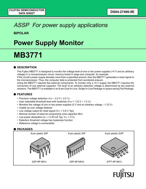
MB3771 Datasheet: Bipolar Power Supply Monitor - Fujitsu
MB3771 Datasheet: Bipolar Power Supply Monitor - Fujitsu
MB3771 Datasheet: Bipolar Power Supply Monitor - Fujitsu
Create successful ePaper yourself
Turn your PDF publications into a flip-book with our unique Google optimized e-Paper software.
<strong>MB3771</strong>■ ABSOLUTE MAXIMUM RATINGSRatingParameter SymbolMinMaxUnit<strong>Power</strong> supply voltage VCC −0.3 +20 VVSA −0.3 VCC + 0.3 ( < +20) VInput voltageVSB −0.3 +20 VVSC −0.3 +20 V<strong>Power</strong> dissipation PD ⎯ 200 (Ta ≤ 85 °C) mWStorage temperature Tstg −55 +125 °CWARNING:Semiconductor devices can be permanently damaged by application of stress (voltage, current,temperature, etc.) in excess of absolute maximum ratings. Do not exceed these ratings.■ RECOMMENDED OPERATING CONDITIONSValueParameterSymbolUnitMinMax<strong>Power</strong> supply voltage VCC 3.5 18 VIRESET 0 20 mAOutput currentIOUTC 0 6 mAOperating ambient temperature Top −40 +85 °CWARNING:The recommended operating conditions are required in order to ensure the normal operation of thesemiconductor device. All of the device’s electrical characteristics are warranted when the device isoperated within these ranges.Always use semiconductor devices within their recommended operating condition ranges. Operationoutside these ranges may adversely affect reliability and could result in device failure.No warranty is made with respect to uses, operating conditions, or combinations not represented onthe data sheet. Users considering application outside the listed conditions are advised to contact theirFUJITSU representatives beforehand.4
<strong>MB3771</strong>■ ELECTRICAL CHARACTERISTICS1. DC CharacteristicsParameter Symbol Conditions<strong>Power</strong> supply current(VCC = 5 V, Ta = + 25 °C)ValueMin Typ MaxUnitICC1 VSB = 5 V, VSC = 0 V ⎯ 350 500 µAICC2 VSB = 0 V, VSC = 0 V ⎯ 400 600 µAVSALVCC 4.10 4.20 4.30 V(DOWN) Ta = −40 °C to +85 °C 4.05 4.20 4.35 VDetection voltageVCC 4.20 4.30 4.40 VVSAH (UP)Ta = −40 °C to +85 °C 4.15 4.30 4.45 VHysterisis width VHYSA ⎯ 50 100 150 mVDetection voltageVSBVSB 1.212 1.230 1.248 VTa = −40 °C to +85 °C 1.200 1.230 1.260 VDeviation of detection voltage ∆VSB VCC = 3.5 V to 18 V ⎯ 3 10 mVHysterisis width VHYSB ⎯ 14 28 42 mVInput currentIIHB VSB = 5 V ⎯ 0 250 nAIILB VSB = 0 V ⎯ 20 250 nAVOHR IRESET = −5 µA, VSB = 5 V 4.5 4.9 ⎯ VOutput voltageIRESET = 3mA, VSB = 0 V ⎯ 0.28 0.4 VVOLRIRESET = 10mA, VSB = 0 V ⎯ 0.38 0.5 VOutput sink current IRESET VOLR = 1.0 V, VSB = 0 V 20 40 ⎯ mACT charge current ICT VSB = 5 V, VCT = 0.5 V 9 12 16 µAInput currentIIHC VSC = 5 V ⎯ 0 500 nAIILC VSC = 0 V ⎯ 50 500 nADetection voltageVSC⎯ 1.225 1.245 1.265 VTa = −40 °C to +85 °C 1.205 1.245 1.285 VDeviation of detection voltage ∆VSC VCC = 3.5 V to 18 V ⎯ 3 10 mVOutput leakage current IOHC VOHC = 18 V ⎯ 0 1 µAOutput voltage VOLC IOUTC = 4 mA, VSC = 5 V ⎯ 0.15 0.4 VOutput sink current IOUTC VOLC = 1.0 V, VSC = 5 V 6 15 ⎯ mAReset operation minimumsupply voltageVCCL VOLR = 0.4 V, IRESET = 200 µA ⎯ 0.8 1.2 V5
<strong>MB3771</strong>2. AC Characteristics(VCC = 5 V, Ta = + 25 °C, CT = 0.01 µF)Parameter Symbol ConditionsValueMin Typ MaxUnitVSA, VSB input pulse width tPI ⎯ 5.0 ⎯ ⎯ µsReset hold time tPO ⎯ 0.5 1.0 1.5 msRESET rise time trRL = 2.2 kΩ,⎯ 1.0 1.5 µsRESET fall time tfCL = 100 pF⎯ 0.1 0.5 µstPD* 1 ⎯ ⎯ 2 10 µsPropagation delay time tPHL* 2RL = 2.2 kΩ,⎯ 0.5 ⎯ µstPLH* 2 CL = 100 pF⎯ 1.0 ⎯ µs*1: In case of VSB termination.*2: In case of VSC termination.6
<strong>MB3771</strong>■ APPLICATION CIRCUIT1. 5V <strong>Power</strong> <strong>Supply</strong> <strong>Monitor</strong><strong>Monitor</strong>ed by VSA. Detection threshold voltage is VSAL and VSAHVCC<strong>MB3771</strong>CT12348765RESETLogiccircuit2. 5V <strong>Power</strong> <strong>Supply</strong> Voltage <strong>Monitor</strong> (Externally Fine-Tuned Type)The VSA detection voltage can be adjusted externally.Resistance R1 and R2 are set sufficiently lower than the IC internal partial voltage resistance, so that the detectionvoltage can be set using the ratio between resistance R1 and R2. (See the table below).•R1, R2 calculation formula (when R1
<strong>MB3771</strong>3. Arbitrary Voltage <strong>Supply</strong> <strong>Monitor</strong>(1) Case: VCC ≤ 18 V• Detection Voltage can be set by R1 and R2.Detection Voltage = (R1 + R2) × VSB/R2• Connect Pin 7 to VCC when VCC less than 4.45 V.• Pin 7 can be opened when VCC greater than 4.45 V<strong>Power</strong> Dissipation can be reduced.Note : Hysteresis of 28 mV at VSB at termination is available.Hysteresis width dose not depend on (R1 + R2).VCC<strong>MB3771</strong>CT12348765R1R2RESET(2) <strong>Monitor</strong>ing VCC > 18 V• Detection Voltage can be set by R1 and R2Detection Voltage = (R1 + R2) × VSB/R2• The RESET signal output is := 0V (low level) and := 5 V (high level). VCC voltage cannot be output.Do not pull up RESET to VCC.• Changing the resistance ratio between R4 and R5 changes the constant voltage output, thereby changing thevoltage of the high level RESET output. Note that the constant voltage output should not exceed 18 V.• The 5 V output can be used as a power supply for control circuits with low current consumption.• In setting the R3 resistance level, caution should be given to the power consumption in the resistor. The tablebelow lists sample resistance values for reference (using 1/4 Ω resistance).VCC (V)Detectionvoltage (V)RESET Output min.power supply voltage (V)R1 (MΩ) R2 (kΩ) R3 (kΩ)Output Current(mA)140 100 6.7 1.6 20 110 < 0.2100 81 3.8 1.3 20 56 < 0.540 33 1.4 0.51 20 11 < 1.6• Values are actual measured values (using IOUTC = 100 µA, VOLC = 0.4 V). Lowering the resistance value of R3reduces the minimum supply voltage of the RESET output, but requires resistance with higher allowable loss.VCCR35 V output(Stablized)CTR4:100 kΩ0.47 µFR5:33 kΩ12348765R1R2RESET8
<strong>MB3771</strong>4. 5 V and 12 V <strong>Power</strong> <strong>Supply</strong> <strong>Monitor</strong> (2 types of power supply monitor VCC1 = 5 V, VCC2 =12 V)• 5 V is monitored by VSA. Detection voltage is about 4.2 V• 12 V is monitored by VSB. When R1 = 390 kΩ and R2 = 62 kΩ, Detection voltage is about 9.0 V.Generally thedetection voltage is determined by the following equation.Detection Voltage = (R1 + R2) × VSB/R2VCC2VCC1<strong>MB3771</strong>CT12348765R1: 390 kΩR2: 62 kΩRESETLogiccircuit5. 5 V and 12 V <strong>Power</strong> <strong>Supply</strong> <strong>Monitor</strong> (RESET signal is generated by 5 V, VCC1 = 5 V, VCC2 = 12 V)• 5 V is monitored by VSA, and generates RESET signal when VSA detects voltage sagging.• 12 V is monitored by VSC, and generates its detection signal at OUTC.• The detection voltage of 12 V monitoring and its hysterisis is determined by the following equations.Detection voltage =R1 + R2 + R3R2 + R3× VSC (8.95 V in the circuit above)Hysterisis width =R1 (R3 − R3 // R4)(R2 + R3) (R2 + R3 // R4)× VSC (200 mV in the circuit above)VCC2VCC1R L: 10 kΩR1: 390 kΩR2: 33 kΩR4: 510 kΩR5: 100 kΩCT1234<strong>MB3771</strong>8765RESETIRQ orPort Logic CircuitR3: 30 kΩ9
<strong>MB3771</strong>6. 5 V <strong>Power</strong> <strong>Supply</strong> <strong>Monitor</strong> with forced RESET input (VCC = 5 V)RESIN is an TTL compatible input.RESINVCC<strong>MB3771</strong>1287RESETCT3465Logic Circuit7. 5 V <strong>Power</strong> <strong>Supply</strong> <strong>Monitor</strong> with Non-inverted RESETIn this case, Comparator C is used to invert RESET signal. OUTC is an open-collector output.RL is used an a pull-up resistor.VCCRESETRL: 10 kΩCT1234<strong>MB3771</strong>87658. <strong>Supply</strong> Voltage <strong>Monitor</strong>ing with Delayed TriggerWhen the voltage shown in the diagram below is applied at VCC, the minimum value of the input pulse width isincreased to 40 µs (when C1 = 1000 pF).The formula for calculating the minimum value of the input pulse width [TPI] is:TPI [µs] := 4 × 10 -2 × C1 [pF]TPVCC5 V4 V<strong>MB3771</strong>CT12348765C1RESET10
<strong>MB3771</strong>9. Dual (Positive/Negative) <strong>Power</strong> <strong>Supply</strong> Voltage <strong>Monitor</strong>ing (VCC = 5 V, VEE = Negative <strong>Power</strong><strong>Supply</strong>)<strong>Monitor</strong>s a 5 V and a negative (any given level) power supply. R1, R2, and R3 should be the same value.Detection Voltage = VSB − VSB × R4/R3Example if VEE = −5 V, R4 = 91 kΩThen the detected voltage = −4.37 VIn cases where VEE may be output when VCC is not output, it is necessary to use a Schottky barrier diode (SBD).VCCR5 : 5.1 kΩ<strong>MB3771</strong>VEER4R3 :20 kΩ123876R1 : 20 kΩRESET0.22 µFCTSBD45R2 : 20 kΩ10. Reference Voltage Generation and Voltage Sagging Detection(1) 9V Reference Voltage Generation and 5V/9V <strong>Monitor</strong>ingDetection Voltage = 7.2 VIn the above examples, the output voltage and the detection voltage are determined by the following equations:Detection Voltage = (R1 + R2) × VSB/R215 VV CC : 5 VR 5 : 3 kΩ<strong>MB3771</strong>0.47 µFCT12348765RESET9 V (≅ 50 mA)R3 :7.5 kΩ R 1: 300 kΩR4 :1.2 kΩR 2: 62 kΩ11
<strong>MB3771</strong>(2) 5 V Reference Voltage Generation and 5V <strong>Monitor</strong>ing (No.1)Detection Voltage = 4.2 VIn the above examples, the output voltage and the detection voltage are determined by the following equations:Output Voltage = (R3 + R4) × VSC/R415 VR5 : 3 kΩ<strong>MB3771</strong>0.47 µFCT12348765R3 : 3.6 kΩRESET5 V(≅ 50 mA)R4 : 1.2 kΩ(3) 5 V Reference Voltage Generation and 5 V <strong>Monitor</strong>ing (No. 2)The value of R1 should be calculated from the current consumption of the <strong>MB3771</strong>, the current flowing at R2 andR3, and the 5 V output current. The table below provides sample resistance values for reference.VCC (V) R1 (kΩ) Output Current (mA)40 11 < 1.624 6.2 < 1.415 4.7 < 0.6VCCR118RESET27GNDCTR2 :100 kΩR3 : 33 kΩ34650.47 µF5 V(4) 1.245 V Reference Voltage Generation and 5 V <strong>Monitor</strong>ingResistor R1 determines Reference current. Using 1.2 kΩ as R1, reference current is about 2 mA.VCC(5 V)R1 : 10 kΩ18RESET27GNDCT0.47 µF3465Reference Voltage1.245 V Typ12
<strong>MB3771</strong>11. Low Voltage and Over Voltage Detection (VCC = 5 V)VSH has no hysteresis. When over voltage is detected, RESET is held in the constant time as well as whenlow voltage is detected.VSL = (R1 + R2) × VSB/R2VSH = (R3 + R4) × VSC/R4VCCR3R1RESETR4CT1234<strong>MB3771</strong>8765R2RESETVSLVSHVCC12. Detection of Abnormal State of <strong>Power</strong> <strong>Supply</strong> System (VCC = 5 V)• This Example circuit detects abnormal low/over voltage of power supply voltage and is indicated by LEDindicator. LED is reset by the CLEAR key.• The detection levels of low/over voltages are determined by VSA, and R1 and R2 respectively.VCCR1R21234<strong>MB3771</strong>8765LEDR3: 620 ΩR4:1 kΩ to 100 kΩCLEAR13
<strong>MB3771</strong>13. Back-up <strong>Power</strong> <strong>Supply</strong> System (VCC = 5 V)• Use CMOS Logic and connect VDD of CMOS logic with VCCO.• The back-up battery works after CS goes high as V2 < V1.• During tPO, memory access is prohibited.• CS‘s threshold voltage V1 is determined by the following equation:V1 = VF + (R1 + R2 + R3) × VSB/R3When V1 is 4.45 V or less, connect 7 pin with VCC.When V1 is 4.45 V or more, 7 pin can be used to open.• The voltage to change V2 is provided as the following equation:V2 = VF + (R1 + R2 + R3) × VSC/ (R2 + R3)However, please set V2 to 3.5 V or more.VCCV1V2CStTPOtVCCOtVCCD1V F0.6 VR4 >1 kΩR 1: 100 kΩR 5: 100 kΩCT123<strong>MB3771</strong>876R 2: 6.2 kΩR 6: 100 kΩVCCO45R3: 56 kΩCS*: Diode has been added to prevent Comp.C from malfunctionig when VCC voltage is low.Set V1 and V2 with care given to VF temperature characteristics (typically negative temperaturecharacteristics).14
<strong>MB3771</strong>■ TYPICAL CHARACTERISTICS<strong>Power</strong> supply current vs. power supply voltageDetection voltage (VSC) vs. anbient temperature<strong>Power</strong> supply current ICC1 (µA)700600500Ta =40025°C300200100−40°C25°C−40°C85°C0085°C5 10 15 20<strong>Power</strong> supply voltage VCC (V)Detection voltage VSC (V)1.301.251.20− 50 −25 0 25 50 75 100Anbient temperature Ta (°C)<strong>Power</strong> supply current vs. power supply voltageDetection voltage (VSB) vs. anbient temperature<strong>Power</strong> supply current ICC2 (µA)700600500Ta = 85°C 25°C400−40°C30020010000−40°C25°C85°C5 10 15 20<strong>Power</strong> supply voltage VCC (V)Detection voltage VSBH,VSBL (V)1.30VSBH1.25VSBL1.20−50 −25 0 25 50 75 100Anbient temperature Ta (°C)Output (RESET) voltage vs. power supply voltageDetection voltage (VSA) vs. anbient temperatureOutput voltage VRESET (V)5432Ta =14.125°C−40°C085°C 4.00 1 2 3 4 5−50 −25 0 25 50 75 100<strong>Power</strong> supply voltage VCC (V)Detection voltage VSAH,VSAL (V)4.54.44.34.2VSAHVSALAnbient temperature Ta (°C)(Continued)15
<strong>MB3771</strong>(Continued)Detection voltage (VSB, VSC) vs. <strong>Power</strong> supply voltageReset voltage (RESET) vs. output currentDetection voltage VSC, VSBL,VSBH (V)1.271.261.25VSBHVSC1.241.23VSBL1.221.211.200 5 10 15 20<strong>Power</strong> supply voltage VCC (V)Output voltage VOHR (V)5.085°C4.5Ta = − 40°C25°C4.00 − 5 −10 −15Output current IRESET (µA)Reset hold time vs. power supply voltage (CT = 0.01µF)Output (RESET) voltage vs. output currentReset hold time tPO (ms)1.5Ta = − 40°C1.025°C85°C0.500 5 10 15 20<strong>Power</strong> supply voltage VCC (V)Output voltage VOLR (V)2.01.00Ta = − 40°C85°C25°C0 10 20 30 40 50Output sink current IRESET (mA)CT pin capacitance vs. reset hold timeOutput voltage (OUTC) vs. output currentReset hold time tPO (s)101100 mTa = 25°C10 m− 40°C1 m100 µ85°C10 µ1.0Ta = − 40°C25°C 85°C0.51 µ01 p 10 p 100 p 1000 p 0.01µ 0.1 µ 1 µ 10 µ 100 µ 0 5 10 15 20CT pin capacitance CT (F)Output sink current IOUTC (mA)Output voltage VOLC (V)16
<strong>MB3771</strong>■ NOTES ON USE• Take account of common impedance when designing the earth line on a printed wiring board.• Take measures against static electricity.- For semiconductors, use antistatic or conductive containers.- When storing or carrying a printed circuit board after chip mounting, put it in a conductive bag or container.- The work table, tools and measuring instruments must be grounded.- The worker must put on a grounding device containing 250 kΩ to 1 MΩ resistors in series.• Do not apply a negative voltage- Applying a negative voltage of −0.3 V or less to an LSI may generate a parasitic transistor, resulting inmalfunction.■ ORDERING INFORMATIONPart number Package Remarks<strong>MB3771</strong>P<strong>MB3771</strong>PS<strong>MB3771</strong>PF8-pin Plastic DIP(DIP-8P-M01)8-pin Plastic SIP(SIP-8P-M03)8-pin Plastic SOP(FPT-8P-M01)17
<strong>MB3771</strong>■ PACKAGE DIMENSIONS8-pin Plastic DIP(DIP-8P-M01)9.40+0.40–0.30+.016.370 –.0121 PIN INDEX 6.20±0.25(.244±.010)4.36(.172)MAX3.00(.118)MIN0.51(.020)MIN0.46±0.08(.018±.003)0.25±0.05(.010±.002)+0.300.99 –01.52 +0.30–0.039 –0+.0120.89 +0.35–0.30+.014.035 –.012+.012.060 –02.54(.100)TYP7.62(.300)TYP15°MAXC1994 FUJITSU LIMITED D08006S-2C-3Dimensions in mm (inches) .Note : The values in parentheses are reference values.(Continued)18
<strong>MB3771</strong>(Continued)8-pin Plastic SIP(SIP-8P-M03)19.65+0.15–0.35+.006.774 –.0143.26±0.25(.128±.010)INDEX-1INDEX-26.20±0.25(.244±.010)8.20±0.30(.323±.012)0.99+0.30–0+.012.039 –04.00±0.30(.157±.012)2.54(.100)1.52 +0.30–0C 1994 FUJITSU LIMITED S08010S-3C-2+.012TYP.060 –00.50±0.08(.020±.003)0.25±0.05(.010±.002)Dimensions in mm (inches) .Note : The values in parentheses are reference values.(Continued)19
<strong>MB3771</strong>(Continued)8-pin Plastic SOP(FPT-8P-M01)Note 1) *1 : These dimensions include resin protrusion.Note 2) *2 : These dimensions do not include resin protrusion.Note 3) Pins width and pins thickness include plating thickness.Note 4) Pins width do not include tie bar cutting remainder.* 1 0.10(.004)+0.256.35 –0.208+.010.250 –.0085+0.030.17 –0.04.007 +.001–.002INDEX5.30±0.30 7.80±0.40(.209±.012) (.307±.016)* 2 Dimensions in mm (inches) .Details of "A" part2.00 +0.25–0.15.079 +.010–.006(Mounting height)1 4"A" 0.25(.010)1.27(.050)0.47±0.08(.019±.003)0.13(.005) M0.10(.004)C 2002 FUJITSU LIMITED F08002S-c-6-70~8˚0.50±0.20(.020±.008)0.60±0.15(.024±.006)0.10 +0.10–0.05+.004–.002.004(Stand off)Note : The values in parentheses are reference values.20
<strong>MB3771</strong>FUJITSU LIMITEDAll Rights Reserved.The contents of this document are subject to change without notice.Customers are advised to consult with FUJITSU salesrepresentatives before ordering.The information, such as descriptions of function and applicationcircuit examples, in this document are presented solely for thepurpose of reference to show examples of operations and uses of<strong>Fujitsu</strong> semiconductor device; <strong>Fujitsu</strong> does not warrant properoperation of the device with respect to use based on suchinformation. When you develop equipment incorporating thedevice based on such information, you must assume anyresponsibility arising out of such use of the information. <strong>Fujitsu</strong>assumes no liability for any damages whatsoever arising out ofthe use of the information.Any information in this document, including descriptions offunction and schematic diagrams, shall not be construed as licenseof the use or exercise of any intellectual property right, such aspatent right or copyright, or any other right of <strong>Fujitsu</strong> or any thirdparty or does <strong>Fujitsu</strong> warrant non-infringement of any third-party’sintellectual property right or other right by using such information.<strong>Fujitsu</strong> assumes no liability for any infringement of the intellectualproperty rights or other rights of third parties which would resultfrom the use of information contained herein.The products described in this document are designed, developedand manufactured as contemplated for general use, includingwithout limitation, ordinary industrial use, general office use,personal use, and household use, but are not designed, developedand manufactured as contemplated (1) for use accompanying fatalrisks or dangers that, unless extremely high safety is secured, couldhave a serious effect to the public, and could lead directly to death,personal injury, severe physical damage or other loss (i.e., nuclearreaction control in nuclear facility, aircraft flight control, air trafficcontrol, mass transport control, medical life support system, missilelaunch control in weapon system), or (2) for use requiringextremely high reliability (i.e., submersible repeater and artificialsatellite).Please note that <strong>Fujitsu</strong> will not be liable against you and/or anythird party for any claims or damages arising in connection withabove-mentioned uses of the products.Any semiconductor devices have an inherent chance of failure. Youmust protect against injury, damage or loss from such failures byincorporating safety design measures into your facility andequipment such as redundancy, fire protection, and prevention ofover-current levels and other abnormal operating conditions.If any products described in this document represent goods ortechnologies subject to certain restrictions on export under theForeign Exchange and Foreign Trade Law of Japan, the priorauthorization by Japanese government will be required for exportof those products from Japan.F0308© FUJITSU LIMITED Printed in Japan


