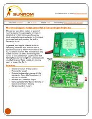
- Page 3 and 4:
ATmega32A2. OverviewThe Atmel ® AV
- Page 5:
ATmega32Ametrical drive characteris
- Page 9 and 10:
ATmega32A6.3.1 SREG - AVR Status Re
- Page 11 and 12:
ATmega32A6.4.1 The X-register, Y-re
- Page 13 and 14:
ATmega32AFigure 6-5.Single Cycle AL
- Page 15:
ATmega32AA return from an interrupt
- Page 18 and 19:
ATmega32AFigure 7-2.Data Memory Map
- Page 20 and 21:
ATmega32AEEPROM data corruption can
- Page 22 and 23:
ATmega32ASupport - Read-While-Write
- Page 24 and 25:
ATmega32AThe next code examples sho
- Page 26 and 27:
ATmega32A8.1.3 Flash Clock - clk FL
- Page 28 and 29:
ATmega32AThe CKSEL0 Fuse together w
- Page 30 and 31:
ATmega32A8.7 Calibrated Internal RC
- Page 32 and 33:
ATmega32A8.10 Register Description8
- Page 34 and 35:
ATmega32Aface, Timer/Counters, Watc
- Page 36 and 37:
ATmega32A9.8.4 Internal Voltage Ref
- Page 38 and 39:
ATmega32A10. System Control and Res
- Page 40 and 41:
ATmega32AFigure 10-3.MCU Start-up,
- Page 42 and 43:
ATmega32AADC is used. To reduce pow
- Page 44 and 45:
ATmega32AThe WDP2, WDP1, and WDP0 b
- Page 46 and 47:
ATmega32Athe case if the Reset Vect
- Page 48 and 49:
ATmega32A$382D out SPL,r16$382E sei
- Page 50 and 51:
ATmega32A12. I/O Ports12.1 Overview
- Page 52 and 53:
ATmega32AIf PORTxn is written logic
- Page 54 and 55:
ATmega32AThe following code example
- Page 56 and 57:
ATmega32AFigure 12-5. Alternate Por
- Page 58 and 59:
ATmega32ATable 12-3.Table 12-4 and
- Page 60 and 61:
ATmega32A• MOSI - Port B, Bit 5MO
- Page 62 and 63:
ATmega32A12.3.3 Alternate Functions
- Page 64 and 65:
ATmega32ATable 12-11. Overriding Si
- Page 66 and 67:
ATmega32A12.4 Register Description1
- Page 68 and 69:
ATmega32A12.4.13 PIND - Port D Inpu
- Page 70 and 71:
ATmega32Alow level interrupt is sel
- Page 73 and 74:
ATmega32A14. 8-bit Timer/Counter0 w
- Page 75 and 76:
ATmega32ASignal description (intern
- Page 77 and 78:
ATmega32Athe OCR0 value, the compar
- Page 79 and 80:
ATmega32AFigure 14-5.CTC Mode, Timi
- Page 81 and 82:
ATmega32AThe PWM resolution for the
- Page 83 and 84:
ATmega32AFigure 14-9. Timer/Counter
- Page 85 and 86:
ATmega32ATable 14-2. Waveform Gener
- Page 87 and 88:
ATmega32AThe Output Compare Registe
- Page 89 and 90:
ATmega32AFigure 15-1.T1/T0 Pin Samp
- Page 91 and 92:
ATmega32A16. 16-bit Timer/Counter11
- Page 93 and 94:
ATmega32Aput Compare Units” on pa
- Page 95 and 96:
ATmega32Athe main code and the inte
- Page 97 and 98:
ATmega32A16.5 Counter UnitThe main
- Page 99 and 100:
ATmega32AThe ICR1 Register can only
- Page 101 and 102:
ATmega32ARegister to either TOP or
- Page 103 and 104:
ATmega32AA change of the COM1x1:0 b
- Page 107:
ATmega32AThe PWM resolution for the
- Page 110:
ATmega32AUsing the ICR1 Register fo
- Page 113 and 114:
ATmega32ATable 16-3 shows the COM1x
- Page 115 and 116:
ATmega32A• Bit 7 - ICNC1: Input C
- Page 117 and 118:
ATmega32AThe Input Capture is updat
- Page 119 and 120:
ATmega32A17. 8-bit Timer/Counter2 w
- Page 121 and 122:
ATmega32AFigure 17-2.DATA BUSCounte
- Page 123 and 124:
ATmega32AThe setup of the OC2 shoul
- Page 125 and 126:
ATmega32AFigure 17-5.CTC Mode, Timi
- Page 127 and 128:
ATmega32A17.7.4 Phase Correct PWM M
- Page 129 and 130:
ATmega32AFigure 17-9. Timer/Counter
- Page 131 and 132:
ATmega32A• If Timer/Counter2 is u
- Page 133 and 134:
ATmega32AA FOC2 strobe will not gen
- Page 135 and 136:
ATmega32A17.11.2 TCNT2 - Timer/Coun
- Page 137 and 138:
ATmega32A17.11.7 SFIOR - Special Fu
- Page 139 and 140:
ATmega32Acommunication cycle when p
- Page 141 and 142:
ATmega32AAssembly Code Example (1)S
- Page 143 and 144:
ATmega32A18.3 SS Pin Functionality1
- Page 145 and 146:
ATmega32A18.3.4 SPSR - SPI Status R
- Page 147 and 148:
ATmega32A19. USART19.1 Features19.2
- Page 149 and 150:
ATmega32A19.2.1 AVR USART vs. AVR U
- Page 151 and 152:
ATmega32ATable 19-1.Operating ModeA
- Page 153 and 154:
ATmega32AThe frame format used by t
- Page 155 and 156:
ATmega32AThe following code example
- Page 157 and 158:
ATmega32AThe Transmit Complete (TXC
- Page 159 and 160:
ATmega32AAssembly Code Example (1)U
- Page 161 and 162:
ATmega32AThe PE bit is set if the n
- Page 163 and 164:
ATmega32AFigure 19-7.Stop Bit Sampl
- Page 165 and 166: ATmega32AIf the receiver is set up
- Page 167 and 168: ATmega32AThe following code example
- Page 169 and 170: ATmega32A• Bit 0 - MPCM: Multi-pr
- Page 171 and 172: ATmega32ATable 19-6.USBS Bit Settin
- Page 173 and 174: ATmega32ATable 19-9.BaudRate(bps)Ex
- Page 175 and 176: ATmega32ATable 19-11.BaudRate(bps)E
- Page 177 and 178: ATmega32A20. Two-wire Serial Interf
- Page 179 and 180: ATmega32Acondition is issued betwee
- Page 181 and 182: ATmega32AFigure 20-6.Typical Data T
- Page 183 and 184: ATmega32AFigure 20-9.Overview of th
- Page 185 and 186: ATmega32A20.6 Using the TWIThe AVR
- Page 187 and 188: ATmega32AAssembly code example C ex
- Page 189 and 190: ATmega32ATable 20-2.Status Code(TWS
- Page 191 and 192: ATmega32AFigure 20-12. Formats and
- Page 193 and 194: ATmega32ATable 20-3.Status Code(TWS
- Page 195 and 196: ATmega32AThe upper seven bits are t
- Page 197 and 198: ATmega32AFigure 20-16. Formats and
- Page 199 and 200: ATmega32ATable 20-5.Status Code(TWS
- Page 201 and 202: ATmega32A4. The transfer must be fi
- Page 203 and 204: ATmega32A20.9.2 TWCR - TWI Control
- Page 205 and 206: ATmega32A20.9.5 TWAR - TWI (Slave)
- Page 207 and 208: ATmega32A21.3 Register Description2
- Page 209 and 210: ATmega32A22. Analog to Digital Conv
- Page 211 and 212: ATmega32AIf differential channels a
- Page 213 and 214: ATmega32Ain ADCSRA. The prescaler k
- Page 215: ATmega32ATable 22-1.ConditionADC Co
- Page 219 and 220: ATmega32AFigure 22-9.ADC Power Conn
- Page 221 and 222: INLATmega32AFigure 22-12. Integral
- Page 223 and 224: ATmega32ATable 22-2.Correlation bet
- Page 225 and 226: ATmega32ATable 22-4.MUX4:011010 ADC
- Page 227 and 228: ATmega32A22.9.4 SFIOR - Special Fun
- Page 229 and 230: ATmega32A• TMS: Test Mode Select.
- Page 231 and 232: ATmega32AThe TMS input must be held
- Page 233 and 234: ATmega32A23.8 Using the JTAG Progra
- Page 235 and 236: ATmega32A24.3.1 Bypass RegisterThe
- Page 237 and 238: ATmega32AThe active states are:•
- Page 239 and 240: ATmega32AFigure 24-4. General Port
- Page 241 and 242: ATmega32AFigure 24-7.Boundary-scan
- Page 243 and 244: ATmega32ATable 24-4.SignalNameBound
- Page 245 and 246: ATmega32ATable 24-5.SignalNameBound
- Page 247 and 248: ATmega32ATable 24-6.Algorithm for U
- Page 249 and 250: ATmega32ATable 24-7. ATmega32A Boun
- Page 251 and 252: ATmega32ATable 24-7. ATmega32A Boun
- Page 253 and 254: ATmega32A25. Boot Loader Support -
- Page 255 and 256: ATmega32AFigure 25-1.Read-While-Wri
- Page 257 and 258: ATmega32Amemory by SPM instruction.
- Page 259 and 260: ATmega32ANotes: 1. The different va
- Page 261 and 262: ATmega32A25.8.8 EEPROM Write Preven
- Page 263 and 264: ATmega32Asbiw loophi:looplo, 2brne
- Page 265 and 266: ATmega32A25.9 Register Description2
- Page 267 and 268:
ATmega32A26. Memory Programming26.1
- Page 269 and 270:
ATmega32ATable 26-4.Fuse Low ByteFu
- Page 271 and 272:
ATmega32ATable 26-7.Signal Name inP
- Page 273 and 274:
ATmega32Achanged. A Chip Erase must
- Page 275 and 276:
ATmega32AFigure 26-3. Programming t
- Page 277 and 278:
ATmega32A3. Set BS1 to “0” and
- Page 279 and 280:
ATmega32A26.7.14 Parallel Programmi
- Page 281 and 282:
ATmega32A26.9 SPI Serial Programmin
- Page 283 and 284:
ATmega32Awithout chip erasing the d
- Page 285 and 286:
ATmega32A26.9.4 SPI Serial Programm
- Page 287 and 288:
ATmega32A• Update-DR: The program
- Page 289 and 290:
ATmega32AFigure 26-14. Programming
- Page 291 and 292:
ATmega32AFigure 26-15. JTAG Program
- Page 293 and 294:
ATmega32AFigure 26-17. Virtual Flas
- Page 295 and 296:
ATmega32A26.10.18 Reading the Flash
- Page 297 and 298:
ATmega32A27. Electrical Characteris
- Page 299 and 300:
ATmega32A27.3 Speed GradesFigure 27
- Page 301 and 302:
ATmega32Aantees that a Brown-out Re
- Page 303 and 304:
ATmega32ATable 27-3. SPI Timing Par
- Page 305 and 306:
ATmega32ATable 27-5. ADC Characteri
- Page 307 and 308:
ATmega32A28. Typical Characteristic
- Page 309 and 310:
ATmega32AFigure 28-4.Active Supply
- Page 311 and 312:
ATmega32AFigure 28-8.Idle Supply Cu
- Page 313 and 314:
ATmega32AFigure 28-12. Idle Supply
- Page 315 and 316:
ATmega32A28.5 Standby Supply Curren
- Page 317 and 318:
ATmega32AFigure 28-20. Reset Pull-u
- Page 319 and 320:
ATmega32AFigure 28-24. I/O Pin Sink
- Page 321 and 322:
ATmega32AFigure 28-28. Reset Input
- Page 323 and 324:
ATmega32AFigure 28-32. BOD Threshol
- Page 325 and 326:
ATmega32AFigure 28-36. Calibrated 8
- Page 327 and 328:
ATmega32AFigure 28-40. Calibrated 4
- Page 329 and 330:
ATmega32AFigure 28-44. Calibrated 1
- Page 331 and 332:
ATmega32AFigure 28-48. ADC Current
- Page 333 and 334:
ATmega32A28.12 Current Consumption
- Page 335 and 336:
ATmega32A29. Register SummaryAddres
- Page 337 and 338:
ATmega32A30. Instruction Set Summar
- Page 339 and 340:
ATmega32AMnemonics Operands Descrip
- Page 341 and 342:
ATmega32A32. Packaging Information3
- Page 343 and 344:
ATmega32A32.3 44M1DMarked Pin# 1 ID
- Page 345 and 346:
ATmega32A34. Datasheet Revision His
- Page 347 and 348:
ATmega32A8.9 Timer/Counter Oscillat
- Page 349 and 350:
ATmega32A18.2 Overview ............
- Page 351 and 352:
ATmega32A26 Memory Programming ....
- Page 353:
Atmel Corporation2325 Orchard Parkw