Quantum Theory of Atoms, Molecules, and Solids
Quantum Theory of Atoms, Molecules, and Solids
Quantum Theory of Atoms, Molecules, and Solids

You also want an ePaper? Increase the reach of your titles
YUMPU automatically turns print PDFs into web optimized ePapers that Google loves.
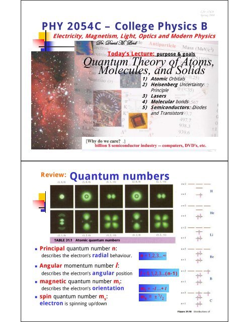
L20—Ch29Spring 2008PHY 2054C – College Physics BElectricity, Magnetism, Light, Optics <strong>and</strong> Modern PhysicsWÜA Wtä|w `A _|ÇwToday’s Lecture: purpose & goals<strong>Quantum</strong> <strong>Theory</strong> <strong>of</strong> <strong>Atoms</strong>,<strong>Molecules</strong>, <strong>and</strong> <strong>Solids</strong>1) Atomic Orbitals2) Heisenberg UncertaintyPrinciple3) Lasers4) Molecular bonds5) Semiconductors: Diodes<strong>and</strong> TransistorsReview:<strong>Quantum</strong> numbers• Principal quantum number n:describes the electron’s radial behaviour.• Angular momentum number l:describes the electron’s angular position• magnetic quantum number m l :describes the electron’s orientationn =1,2,3…∞l =0,1,2,3…(n-1)m l = -l …+l• spin quantum number m s: m s = ± 1 / 2electron is spinning up/down
Laserslight amplification by stimulated emission <strong>of</strong> radiation; metastable because l = ±1; collisions opposite l’ s all in-phase,, highly polarizedLaserslight amplification by stimulated emission <strong>of</strong> radiatione.g. HeNe laser (red light)• we all have a holograph in our pocket (thetiny iridescent images on right <strong>of</strong> VISA<strong>and</strong> Mastercard credit cards)• very complex interference pattern created byinterference <strong>of</strong> laser light <strong>of</strong>f the 3-dimensional object.
Covalent Molecular BondsS=0S=1++- + +-+ +-• Covalent bonds form by sharing <strong>of</strong> electronsbetween atoms. Spin becomes very important;• Each electron must have different quantumnumbers, which favours ↑↓ over ↑↑.• Allows identical spacial distribution, true “sharing”<strong>of</strong> electrons• Binding comes from +- electric attraction.• Binding Energy large! e.g. 7.4 eV (Diamond)Ionic Molecular Bonds• Ionic Bonds are covalent bonds, where electrons‘prefer’ one <strong>of</strong> the atoms.• Na, 3 valence e - , wants to be Ne with 2 e -• Cl, 7 valence e - ,wants to be Ar with 8 e - ,• Cl can “borrow” an electronfrom Na <strong>and</strong> both becomequasi-noble gases• Binding comes from electric attraction between the Na +<strong>and</strong> Cl -• Very Strong binding!! Energy 7.8 eV NaCl
Molecularvan-der-Waals bonds• Attraction between <strong>Molecules</strong> with permanentDipole-moments.• Usually quite weak, but somewhatstronger for Hydrogen-bond.• Binding energy around 0.03 – 0.3 eVMetallic Bond• Metals have free moving electrons, which areshared by all the atoms.• Electrons between positiveIons lead to electricattraction.• Binding Energy:1 to 3 eV• Compare Binding Energy to “Work Function”in photo-electric effect
Potential Energy in <strong>Molecules</strong>Distancebetween <strong>Atoms</strong>• All sorts <strong>of</strong> binding lead to a potential energy curve, with an“optimum” distance between atoms at the lowestpotenial energy• Most atoms need to overcome a P.E. barrier to form aMolecule –this is the activation energy for reactionB<strong>and</strong> <strong>Theory</strong> <strong>of</strong> <strong>Solids</strong>• Every state in a Single Atom leads to two states ina Molecule, one S=0, one S=1.• Many <strong>Atoms</strong> Many states.• Solid State crystal energy b<strong>and</strong>s• “Energy gap” will be found between b<strong>and</strong>s <strong>of</strong> differentatomic symmetry
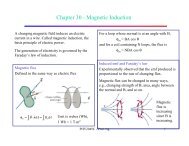
B<strong>and</strong> Gap <strong>and</strong> Conductivity• Valence B<strong>and</strong>: b<strong>and</strong> created from valence (bound) electrons• Conduction B<strong>and</strong>: electrons in conduction b<strong>and</strong> are not tiedto individual atoms, but are free to move around.• B<strong>and</strong> gap:a) 5eV: Insulator⇒ very difficult!!c) ~1eV Semiconductor⇒ could be pushedwith voltage or kT!!• Semiconductors:• Germanium, Silicon, GaAs, ...Conduction b<strong>and</strong>lowest empty (mobile) stateshighest filled e- statesValence b<strong>and</strong>lowest empty (mobile) stateshighest filled e- stateslowest empty (mobile) stateshighest filled e- statesSemiconductors <strong>and</strong> Doping• You can “dope” semiconductors (i.e. add extra chargecarriers) by adding a small concentration <strong>of</strong> impurities tobecome conductors <strong>of</strong> either positive or negative charges;• (No net charge is added;• e.g. Arsenic has extra e - ,extrap + , but the electron easily moves around,‘acts like’ a silicon atom with one extra electron• e.g. Gallium has one fewer e - ,one fewerp + , ‘acts like’ a silicon atom withone to few electrons (a ‘hole’), which also easily moves around• Extra electrons “n-type” or extra “holes” “p-type”n-typep-type“moving hole”
Semiconductor Diodes• The simplest application <strong>of</strong> dopedsemiconductors is the pn-junctiondiode.• Contact between regions <strong>of</strong> p-doped<strong>and</strong> n-doped Silicon.• a) apply voltage p+ n-: + holes movetoward n-zone - electrons toward p-zone→ brought closer together <strong>and</strong> thusrecombine → current flow+ + + ++ + + +––––––––––––––––––• b) apply voltage opposite direction:holes <strong>and</strong> electrons are pushed fartherapart → cannot recombine → nocurrent flow+ region + + <strong>of</strong> ++ ––––– + + +no charge–––– carriers–––––Characteristics <strong>of</strong> pn- junction• At the junction, the electrons will fallinto the neighboring holes, each gainingthe “b<strong>and</strong> gap” 0.6 eV in energy.• The process stops because the surpluscharge creates an opposing electricfield <strong>of</strong> 0.6 Vp- - -- - - - -++ + + + + + +np+ n-Diode symbolPE (e - )b<strong>and</strong>-gap <strong>of</strong>semiconductor=p-type• Notice that current will ΔV = “b<strong>and</strong> gap”flow from from p+ to n-=0.6 V n-typewhen voltage bias is in that direction.• But current will not flow in the reverse bias direction.
Photo-Diode, Solar Cell• When a photon has energyE γ> 0.6 eV, (<strong>and</strong> visible light isfrom ~2-5ev)it can lift an electron from thevalence into the conductionb<strong>and</strong>.• Inside junction-field;electron, hole gainenergy <strong>of</strong> at least 0.6 eV, current flows• Convert photon E γinto electric U (energy)p-typep- - - - - - - -+ -+ + + + + + + +n“b<strong>and</strong> gap”=0.6 VPE (e - )+-n-typeDiode bridgeinput signalAC signalinputoutputforward biasoutputreverse biasforward biasreverse biasinputadded together
(bipolar junction) Transistors• 2 pn junctions ‘back-to-back’,BE-forward biasedCB-reverse biasedAmplifier:I C~100 I Breversebiasedforwardbiased++npn-• The base is so weakly doped <strong>and</strong> thin, that only ~1%<strong>of</strong> the electrons recombine with a hole in the base.• As minority carriers, the other 99% are now free topass the reverse biased BC-junction creating anamplifier.