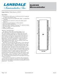
Interfacing the M68HC05 MCU to the MC145051 A/D Converter
Interfacing the M68HC05 MCU to the MC145051 A/D Converter
Interfacing the M68HC05 MCU to the MC145051 A/D Converter

You also want an ePaper? Increase the reach of your titles
YUMPU automatically turns print PDFs into web optimized ePapers that Google loves.
Freescale Semiconduc<strong>to</strong>r, Inc.Application NoteThe following example is provided <strong>to</strong> test <strong>the</strong> software routine. Follow<strong>the</strong>se steps after programming <strong>the</strong> MC68HC705C8 with <strong>the</strong> code inAppendix C — MC68HC705C8/<strong>MC145051</strong> Assembly Code andconstructing <strong>the</strong> schematic in Appendix A —MC68HC705C8/<strong>MC145051</strong> Schematic.1. Set <strong>the</strong> potentiometer <strong>to</strong> a reading of 2.20 volts.2. If V REF –V AG is exactly 5.00 volts, <strong>the</strong> A/D should convert <strong>to</strong> areading of 450 or $1C2. (See Figure 4.)nc...Freescale Semiconduc<strong>to</strong>r, I3. Power on <strong>the</strong> circuit.4. The A/D value will be outputted on port B and port C. This value is<strong>the</strong> previously converted value. Since <strong>the</strong>re was no previousconversion, <strong>the</strong> data will be garbage.5. Pull <strong>the</strong> RESET pin low and <strong>the</strong>n high. The routine will run again,and <strong>the</strong> previous value of <strong>the</strong> AN0 channel conversion isrepresented on port B and port C. The value for port B should be$70 and port C should be $80. The result might differ by a leastsignificant bit (LSB). (See Figure 7.)This routine is <strong>the</strong> simplest example <strong>to</strong> test and learn <strong>the</strong> interface from<strong>the</strong> MC68HC705C8 <strong>to</strong> <strong>the</strong> <strong>MC145051</strong>. Notice that <strong>the</strong> mux address mustbe in <strong>the</strong> high nibble of <strong>the</strong> byte before it is written <strong>to</strong> <strong>the</strong> SPI dataregister. Also, since this routine was hard-coded, <strong>the</strong> A/D channel wasalready known and written in<strong>to</strong> memory. The code can be easily adaptedas a subroutine, which requires that <strong>the</strong> channel <strong>to</strong> be converted is aninput <strong>to</strong> <strong>the</strong> subroutine. If <strong>the</strong> application requires that successive A/Dconversions are made, make sure that <strong>the</strong> <strong>MC145051</strong> has enough time<strong>to</strong> convert <strong>the</strong> present channel before initializing ano<strong>the</strong>r conversion. Ifneeded, <strong>the</strong> <strong>MC145051</strong> provides <strong>the</strong> EOC pin. During a conversionprocess, <strong>the</strong> pin is held low. After conversion is complete, <strong>the</strong> pin isdriven high. Ano<strong>the</strong>r port pin on <strong>the</strong> MC68HC705C8 might be used <strong>to</strong>read <strong>the</strong> EOC pin.AN1228 — Rev. 2.012 MOTOROLAFor More Information On This Product,Go <strong>to</strong>: www.freescale.com