Access line, 16 MHz STM8S 8-bit MCU, up to 8 Kbytes Flash, data ...
Access line, 16 MHz STM8S 8-bit MCU, up to 8 Kbytes Flash, data ...
Access line, 16 MHz STM8S 8-bit MCU, up to 8 Kbytes Flash, data ...
- No tags were found...

Create successful ePaper yourself
Turn your PDF publications into a flip-book with our unique Google optimized e-Paper software.
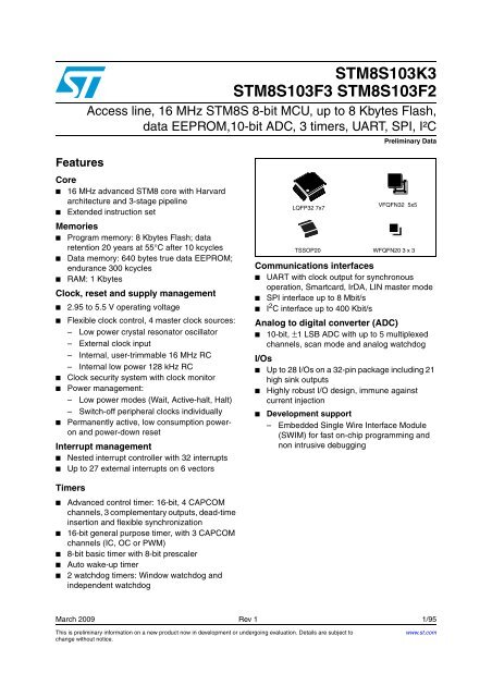
<strong>STM8S</strong>103K3<strong>STM8S</strong>103F3 <strong>STM8S</strong>103F2<strong>Access</strong> <strong>line</strong>, <strong>16</strong> <strong>MHz</strong> <strong>STM8S</strong> 8-<strong>bit</strong> <strong>MCU</strong>, <strong>up</strong> <strong>to</strong> 8 <strong>Kbytes</strong> <strong>Flash</strong>,<strong>data</strong> EEPROM,10-<strong>bit</strong> ADC, 3 timers, UART, SPI, I²CPreliminary DataFeaturesCore■ <strong>16</strong> <strong>MHz</strong> advanced STM8 core with Harvardarchitecture and 3-stage pipe<strong>line</strong>■ Extended instruction setMemories■ Program memory: 8 <strong>Kbytes</strong> <strong>Flash</strong>; <strong>data</strong>retention 20 years at 55°C after 10 kcycles■ Data memory: 640 bytes true <strong>data</strong> EEPROM;endurance 300 kcycles■ RAM: 1 <strong>Kbytes</strong>Clock, reset and s<strong>up</strong>ply management■ 2.95 <strong>to</strong> 5.5 V operating voltage■ Flexible clock control, 4 master clock sources:– Low power crystal resona<strong>to</strong>r oscilla<strong>to</strong>r– External clock input– Internal, user-trimmable <strong>16</strong> <strong>MHz</strong> RC– Internal low power 128 kHz RC■ Clock security system with clock moni<strong>to</strong>r■ Power management:– Low power modes (Wait, Active-halt, Halt)– Switch-off peripheral clocks individually■ Permanently active, low consumption poweronand power-down resetInterr<strong>up</strong>t management■ Nested interr<strong>up</strong>t controller with 32 interr<strong>up</strong>ts■ Up <strong>to</strong> 27 external interr<strong>up</strong>ts on 6 vec<strong>to</strong>rsLQFP32 7x7VFQFN32 5x5TSSOP20 WFQFN20 3 x 3Communications interfaces■ UART with clock output for synchronousoperation, Smartcard, IrDA, LIN master mode■ SPI interface <strong>up</strong> <strong>to</strong> 8 M<strong>bit</strong>/s■ I 2 C interface <strong>up</strong> <strong>to</strong> 400 K<strong>bit</strong>/sAnalog <strong>to</strong> digital converter (ADC)■ 10-<strong>bit</strong>, ±1 LSB ADC with <strong>up</strong> <strong>to</strong> 5 multiplexedchannels, scan mode and analog watchdogI/Os■ Up <strong>to</strong> 28 I/Os on a 32-pin package including 21high sink outputs■ Highly robust I/O design, immune againstcurrent injection■ Development s<strong>up</strong>port– Embedded Single Wire Interface Module(SWIM) for fast on-chip programming andnon intrusive debuggingTimers■■■■■Advanced control timer: <strong>16</strong>-<strong>bit</strong>, 4 CAPCOMchannels, 3 complementary outputs, dead-timeinsertion and flexible synchronization<strong>16</strong>-<strong>bit</strong> general purpose timer, with 3 CAPCOMchannels (IC, OC or PWM)8-<strong>bit</strong> basic timer with 8-<strong>bit</strong> prescalerAu<strong>to</strong> wake-<strong>up</strong> timer2 watchdog timers: Window watchdog andindependent watchdogMarch 2009 Rev 1 1/95This is preliminary information on a new product now in development or undergoing evaluation. Details are subject <strong>to</strong>change without notice.www.st.com1
Contents<strong>STM8S</strong>103xContents1 Introduction . . . . . . . . . . . . . . . . . . . . . . . . . . . . . . . . . . . . . . . . . . . . . . . . 92 Description . . . . . . . . . . . . . . . . . . . . . . . . . . . . . . . . . . . . . . . . . . . . . . . . 103 Block diagram . . . . . . . . . . . . . . . . . . . . . . . . . . . . . . . . . . . . . . . . . . . . . 114 Product overview . . . . . . . . . . . . . . . . . . . . . . . . . . . . . . . . . . . . . . . . . . 124.1 Central processing unit STM8 . . . . . . . . . . . . . . . . . . . . . . . . . . . . . . . . . 124.2 Single wire interface module (SWIM) and debug module (DM) . . . . . . . . 134.3 Interr<strong>up</strong>t controller . . . . . . . . . . . . . . . . . . . . . . . . . . . . . . . . . . . . . . . . . . 134.4 <strong>Flash</strong> program and <strong>data</strong> EEPROM memory . . . . . . . . . . . . . . . . . . . . . . . 144.5 Clock controller . . . . . . . . . . . . . . . . . . . . . . . . . . . . . . . . . . . . . . . . . . . . . 154.6 Power management . . . . . . . . . . . . . . . . . . . . . . . . . . . . . . . . . . . . . . . . . 154.7 Watchdog timers . . . . . . . . . . . . . . . . . . . . . . . . . . . . . . . . . . . . . . . . . . . <strong>16</strong>4.8 Au<strong>to</strong> wake<strong>up</strong> counter . . . . . . . . . . . . . . . . . . . . . . . . . . . . . . . . . . . . . . . . <strong>16</strong>4.9 Beeper . . . . . . . . . . . . . . . . . . . . . . . . . . . . . . . . . . . . . . . . . . . . . . . . . . . 174.10 TIM1 - <strong>16</strong>-<strong>bit</strong> advanced control timer . . . . . . . . . . . . . . . . . . . . . . . . . . . . 174.11 TIM2 - <strong>16</strong>-<strong>bit</strong> general purpose timer . . . . . . . . . . . . . . . . . . . . . . . . . . . . . 174.12 TIM4 - 8-<strong>bit</strong> basic timer . . . . . . . . . . . . . . . . . . . . . . . . . . . . . . . . . . . . . . . 174.13 Analog-<strong>to</strong>-digital converter (ADC1) . . . . . . . . . . . . . . . . . . . . . . . . . . . . . 184.14 Communication interfaces . . . . . . . . . . . . . . . . . . . . . . . . . . . . . . . . . . . . 184.14.1 UART1 . . . . . . . . . . . . . . . . . . . . . . . . . . . . . . . . . . . . . . . . . . . . . . . . . . 184.14.2 SPI . . . . . . . . . . . . . . . . . . . . . . . . . . . . . . . . . . . . . . . . . . . . . . . . . . . . . 194.14.3 I 2 C . . . . . . . . . . . . . . . . . . . . . . . . . . . . . . . . . . . . . . . . . . . . . . . . . . . . . 195 Pinout and pin description . . . . . . . . . . . . . . . . . . . . . . . . . . . . . . . . . . . 205.0.1 Alternate function remapping . . . . . . . . . . . . . . . . . . . . . . . . . . . . . . . . . 295.0.2 Interr<strong>up</strong>t vec<strong>to</strong>r mapping . . . . . . . . . . . . . . . . . . . . . . . . . . . . . . . . . . . . 296 Option bytes . . . . . . . . . . . . . . . . . . . . . . . . . . . . . . . . . . . . . . . . . . . . . . 317 Memory and register map . . . . . . . . . . . . . . . . . . . . . . . . . . . . . . . . . . . 357.1 Memory map . . . . . . . . . . . . . . . . . . . . . . . . . . . . . . . . . . . . . . . . . . . . . . 352/95
<strong>STM8S</strong>103xContents7.2 Register map . . . . . . . . . . . . . . . . . . . . . . . . . . . . . . . . . . . . . . . . . . . . . . 368 Electrical characteristics . . . . . . . . . . . . . . . . . . . . . . . . . . . . . . . . . . . . 468.1 Parameter conditions . . . . . . . . . . . . . . . . . . . . . . . . . . . . . . . . . . . . . . . . 468.1.1 Minimum and maximum values . . . . . . . . . . . . . . . . . . . . . . . . . . . . . . . 468.1.2 Typical values . . . . . . . . . . . . . . . . . . . . . . . . . . . . . . . . . . . . . . . . . . . . . 468.1.3 Typical curves . . . . . . . . . . . . . . . . . . . . . . . . . . . . . . . . . . . . . . . . . . . . 468.1.4 Loading capaci<strong>to</strong>r . . . . . . . . . . . . . . . . . . . . . . . . . . . . . . . . . . . . . . . . . 468.1.5 Pin input voltage . . . . . . . . . . . . . . . . . . . . . . . . . . . . . . . . . . . . . . . . . . 478.2 Absolute maximum ratings . . . . . . . . . . . . . . . . . . . . . . . . . . . . . . . . . . . . 478.3 Operating conditions . . . . . . . . . . . . . . . . . . . . . . . . . . . . . . . . . . . . . . . . 498.3.1 VCAP external capaci<strong>to</strong>r . . . . . . . . . . . . . . . . . . . . . . . . . . . . . . . . . . . . 508.3.2 S<strong>up</strong>ply current characteristics . . . . . . . . . . . . . . . . . . . . . . . . . . . . . . . . 518.3.3 External clock sources and timing characteristics . . . . . . . . . . . . . . . . . 598.3.4 Internal clock sources and timing characteristics . . . . . . . . . . . . . . . . . 628.3.5 Memory characteristics . . . . . . . . . . . . . . . . . . . . . . . . . . . . . . . . . . . . . 648.3.6 I/O port pin characteristics . . . . . . . . . . . . . . . . . . . . . . . . . . . . . . . . . . . 658.3.7 Reset pin characteristics . . . . . . . . . . . . . . . . . . . . . . . . . . . . . . . . . . . . 708.3.8 SPI serial peripheral interface . . . . . . . . . . . . . . . . . . . . . . . . . . . . . . . . 728.3.9 I 2 C interface characteristics . . . . . . . . . . . . . . . . . . . . . . . . . . . . . . . . . . 758.3.10 10-<strong>bit</strong> ADC characteristics . . . . . . . . . . . . . . . . . . . . . . . . . . . . . . . . . . . 768.3.11 EMC characteristics . . . . . . . . . . . . . . . . . . . . . . . . . . . . . . . . . . . . . . . . 798.4 Thermal characteristics . . . . . . . . . . . . . . . . . . . . . . . . . . . . . . . . . . . . . . 828.4.1 Reference document . . . . . . . . . . . . . . . . . . . . . . . . . . . . . . . . . . . . . . . 828.4.2 Selecting the product temperature range . . . . . . . . . . . . . . . . . . . . . . . . 839 Package characteristics . . . . . . . . . . . . . . . . . . . . . . . . . . . . . . . . . . . . . 849.1 Package mechanical <strong>data</strong> . . . . . . . . . . . . . . . . . . . . . . . . . . . . . . . . . . . . 859.1.1 LQFP package mechanical <strong>data</strong> . . . . . . . . . . . . . . . . . . . . . . . . . . . . . . 859.1.2 QFN package mechanical <strong>data</strong> . . . . . . . . . . . . . . . . . . . . . . . . . . . . . . . 869.1.3 TSSOP package mechanical <strong>data</strong> . . . . . . . . . . . . . . . . . . . . . . . . . . . . . 879.1.4 WFQFPN20 package mechanical <strong>data</strong> . . . . . . . . . . . . . . . . . . . . . . . . . 8810 Ordering information . . . . . . . . . . . . . . . . . . . . . . . . . . . . . . . . . . . . . . . 9111 STM8 development <strong>to</strong>ols . . . . . . . . . . . . . . . . . . . . . . . . . . . . . . . . . . . . 9211.1 Emulation and in-circuit debugging <strong>to</strong>ols . . . . . . . . . . . . . . . . . . . . . . . . . 923/95
Contents<strong>STM8S</strong>103x11.2 Software <strong>to</strong>ols . . . . . . . . . . . . . . . . . . . . . . . . . . . . . . . . . . . . . . . . . . . . . . 9311.2.1 STM8 <strong>to</strong>olset . . . . . . . . . . . . . . . . . . . . . . . . . . . . . . . . . . . . . . . . . . . . . 9311.2.2 C and assembly <strong>to</strong>olchains . . . . . . . . . . . . . . . . . . . . . . . . . . . . . . . . . . 9311.3 Programming <strong>to</strong>ols . . . . . . . . . . . . . . . . . . . . . . . . . . . . . . . . . . . . . . . . . . 9312 Revision his<strong>to</strong>ry . . . . . . . . . . . . . . . . . . . . . . . . . . . . . . . . . . . . . . . . . . . 944/95
<strong>STM8S</strong>103xList of tablesList of tablesTable 1. <strong>STM8S</strong>103x <strong>Access</strong> <strong>line</strong> features. . . . . . . . . . . . . . . . . . . . . . . . . . . . . . . . . . . . . . . . . . . . 10Table 2. TIM timer features. . . . . . . . . . . . . . . . . . . . . . . . . . . . . . . . . . . . . . . . . . . . . . . . . . . . . . . . 17Table 3. Legend/abbreviations . . . . . . . . . . . . . . . . . . . . . . . . . . . . . . . . . . . . . . . . . . . . . . . . . . . . . 21Table 4. VQFN32/LQFP32 pin description . . . . . . . . . . . . . . . . . . . . . . . . . . . . . . . . . . . . . . . . . . . . 21Table 5. <strong>STM8S</strong>103F pin description . . . . . . . . . . . . . . . . . . . . . . . . . . . . . . . . . . . . . . . . . . . . . . . . 26Table 6. Pin-<strong>to</strong>-pin comparison of pin 7 <strong>to</strong> 12 in 32-pin access <strong>line</strong> devices . . . . . . . . . . . . . . . . . . 28Table 7. Interr<strong>up</strong>t mapping . . . . . . . . . . . . . . . . . . . . . . . . . . . . . . . . . . . . . . . . . . . . . . . . . . . . . . . . 29Table 8. Option bytes . . . . . . . . . . . . . . . . . . . . . . . . . . . . . . . . . . . . . . . . . . . . . . . . . . . . . . . . . . . . 31Table 9. Option byte description . . . . . . . . . . . . . . . . . . . . . . . . . . . . . . . . . . . . . . . . . . . . . . . . . . . . 32Table 10. <strong>STM8S</strong>103K alternate function remapping <strong>bit</strong>s . . . . . . . . . . . . . . . . . . . . . . . . . . . . . . . . . 33Table 11. <strong>STM8S</strong>103F alternate function remapping <strong>bit</strong>s . . . . . . . . . . . . . . . . . . . . . . . . . . . . . . . . . 34Table 12. I/O port hardware register map. . . . . . . . . . . . . . . . . . . . . . . . . . . . . . . . . . . . . . . . . . . . . . 36Table 13. General hardware register map . . . . . . . . . . . . . . . . . . . . . . . . . . . . . . . . . . . . . . . . . . . . . 37Table 14. CPU/SWIM/debug module/interr<strong>up</strong>t controller registers. . . . . . . . . . . . . . . . . . . . . . . . . . . 44Table 15. Voltage characteristics . . . . . . . . . . . . . . . . . . . . . . . . . . . . . . . . . . . . . . . . . . . . . . . . . . . . 47Table <strong>16</strong>. Current characteristics . . . . . . . . . . . . . . . . . . . . . . . . . . . . . . . . . . . . . . . . . . . . . . . . . . . . 48Table 17. Thermal characteristics. . . . . . . . . . . . . . . . . . . . . . . . . . . . . . . . . . . . . . . . . . . . . . . . . . . . 48Table 18. General operating conditions . . . . . . . . . . . . . . . . . . . . . . . . . . . . . . . . . . . . . . . . . . . . . . . 49Table 19. Operating conditions at power-<strong>up</strong>/power-down . . . . . . . . . . . . . . . . . . . . . . . . . . . . . . . . . 49Table 20. Total current consumption with code execution in run mode at V DD = 5.0 V . . . . . . . . . . . 51Table 21. Total current consumption with code execution in run mode at V DD = 3.3 V . . . . . . . . . . . 52Table 22. Total current consumption in Wait mode at V DD = 5.0 V . . . . . . . . . . . . . . . . . . . . . . . . . . 53Table 23. Total current consumption in Wait mode at V DD = 3.3 V . . . . . . . . . . . . . . . . . . . . . . . . . . 53Table 24. Total current consumption in active halt mode at V DD = 5.0 V, T A -40 <strong>to</strong> 85° C. . . . . . . . . 54Table 25. Total current consumption in active halt mode at V DD = 3.3 V . . . . . . . . . . . . . . . . . . . . . . 54Table 26. Total current consumption in halt mode at V DD = 5.0 V, T A -40 <strong>to</strong> 85° C . . . . . . . . . . . . . . 55Table 27. Total current consumption in halt mode at V DD = 3.3 V . . . . . . . . . . . . . . . . . . . . . . . . . . . 55Table 28. Wake<strong>up</strong> times . . . . . . . . . . . . . . . . . . . . . . . . . . . . . . . . . . . . . . . . . . . . . . . . . . . . . . . . . . . 56Table 29. Total current consumption and timing in forced reset state . . . . . . . . . . . . . . . . . . . . . . . . 56Table 30. Peripheral current consumption . . . . . . . . . . . . . . . . . . . . . . . . . . . . . . . . . . . . . . . . . . . . . 57Table 31. HSE user external clock characteristics . . . . . . . . . . . . . . . . . . . . . . . . . . . . . . . . . . . . . . . 59Table 32. HSE oscilla<strong>to</strong>r characteristics . . . . . . . . . . . . . . . . . . . . . . . . . . . . . . . . . . . . . . . . . . . . . . . 60Table 33. HSI oscilla<strong>to</strong>r characteristics. . . . . . . . . . . . . . . . . . . . . . . . . . . . . . . . . . . . . . . . . . . . . . . . 62Table 34. LSI oscilla<strong>to</strong>r characteristics . . . . . . . . . . . . . . . . . . . . . . . . . . . . . . . . . . . . . . . . . . . . . . . . 63Table 35. RAM and hardware registers . . . . . . . . . . . . . . . . . . . . . . . . . . . . . . . . . . . . . . . . . . . . . . . 64Table 36. <strong>Flash</strong> program memory/<strong>data</strong> EEPROM memory . . . . . . . . . . . . . . . . . . . . . . . . . . . . . . . . 64Table 37. I/O static characteristics . . . . . . . . . . . . . . . . . . . . . . . . . . . . . . . . . . . . . . . . . . . . . . . . . . . 65Table 38. Output driving current (standard ports). . . . . . . . . . . . . . . . . . . . . . . . . . . . . . . . . . . . . . . . 67Table 39. Output driving current (true open drain ports). . . . . . . . . . . . . . . . . . . . . . . . . . . . . . . . . . . 67Table 40. Output driving current (high sink ports). . . . . . . . . . . . . . . . . . . . . . . . . . . . . . . . . . . . . . . . 67Table 41. NRST pin characteristics . . . . . . . . . . . . . . . . . . . . . . . . . . . . . . . . . . . . . . . . . . . . . . . . . . 70Table 42. SPI characteristics . . . . . . . . . . . . . . . . . . . . . . . . . . . . . . . . . . . . . . . . . . . . . . . . . . . . . . . 72Table 43. I 2 C characteristics. . . . . . . . . . . . . . . . . . . . . . . . . . . . . . . . . . . . . . . . . . . . . . . . . . . . . . . . 75Table 44. ADC characteristics . . . . . . . . . . . . . . . . . . . . . . . . . . . . . . . . . . . . . . . . . . . . . . . . . . . . . . 76Table 45. ADC accuracy with R AIN < 10 kΩ R AIN , V DD = 3.3 V . . . . . . . . . . . . . . . . . . . . . . . . . . . . . 77Table 46. ADC accuracy with R AIN < 10 kΩ , V DD = 5 V. . . . . . . . . . . . . . . . . . . . . . . . . . . . . . . . . . . 77Table 47. EMS <strong>data</strong> . . . . . . . . . . . . . . . . . . . . . . . . . . . . . . . . . . . . . . . . . . . . . . . . . . . . . . . . . . . . . . 80Table 48. EMI <strong>data</strong> . . . . . . . . . . . . . . . . . . . . . . . . . . . . . . . . . . . . . . . . . . . . . . . . . . . . . . . . . . . . . . . 805/95
List of tables<strong>STM8S</strong>103xTable 49. ESD absolute maximum ratings . . . . . . . . . . . . . . . . . . . . . . . . . . . . . . . . . . . . . . . . . . . . . 81Table 50. Electrical sensitivities . . . . . . . . . . . . . . . . . . . . . . . . . . . . . . . . . . . . . . . . . . . . . . . . . . . . . 81Table 51. Thermal characteristics. . . . . . . . . . . . . . . . . . . . . . . . . . . . . . . . . . . . . . . . . . . . . . . . . . . . 82Table 52. 32-pin low profile quad flat package mechanical <strong>data</strong> . . . . . . . . . . . . . . . . . . . . . . . . . . . . 85Table 53. 32-lead very thin fine pitch quad flat no-lead package mechanical <strong>data</strong> . . . . . . . . . . . . . . 86Table 54. TSSOP 20-pin, 4.40 mm body, 0.65 mm pitch mechanical <strong>data</strong> . . . . . . . . . . . . . . . . . . . . 87Table 55. 20-lead very very thin fine pitch quad flat no-lead package (3 x 3), packagemechanical <strong>data</strong>. . . . . . . . . . . . . . . . . . . . . . . . . . . . . . . . . . . . . . . . . . . . . . . . . . . . . . . . . 89Table 56. Document revision his<strong>to</strong>ry . . . . . . . . . . . . . . . . . . . . . . . . . . . . . . . . . . . . . . . . . . . . . . . . . 946/95
<strong>STM8S</strong>103xList of figuresList of figuresFigure 1. Block diagram . . . . . . . . . . . . . . . . . . . . . . . . . . . . . . . . . . . . . . . . . . . . . . . . . . . . . . . . . . . 11Figure 2. <strong>Flash</strong> memory organisation . . . . . . . . . . . . . . . . . . . . . . . . . . . . . . . . . . . . . . . . . . . . . . . . 14Figure 3. <strong>STM8S</strong>103K VQFN32/LQFP32 pinout . . . . . . . . . . . . . . . . . . . . . . . . . . . . . . . . . . . . . . . . 20Figure 4. <strong>STM8S</strong>103F TSSOP 20-pin pinout. . . . . . . . . . . . . . . . . . . . . . . . . . . . . . . . . . . . . . . . . . . 24Figure 5. <strong>STM8S</strong>103F WFQFPN package pinout . . . . . . . . . . . . . . . . . . . . . . . . . . . . . . . . . . . . . . . 25Figure 6. Memory map. . . . . . . . . . . . . . . . . . . . . . . . . . . . . . . . . . . . . . . . . . . . . . . . . . . . . . . . . . . . 35Figure 7. Pin loading conditions. . . . . . . . . . . . . . . . . . . . . . . . . . . . . . . . . . . . . . . . . . . . . . . . . . . . . 46Figure 8. Pin input voltage . . . . . . . . . . . . . . . . . . . . . . . . . . . . . . . . . . . . . . . . . . . . . . . . . . . . . . . . . 47Figure 9. f CPUmax versus V DD . . . . . . . . . . . . . . . . . . . . . . . . . . . . . . . . . . . . . . . . . . . . . . . . . . . . . . . . . . . . . . . . . . . . . 49Figure 10. External capaci<strong>to</strong>r . . . . . . . . . . . . . . . . . . . . . . . . . . . . . . . . . . . . . . . . . . . . . . . . . . . . . . . . 50Figure 11. Typ. IDD(RUN)HSE vs. VDD @ fCPU = <strong>16</strong> <strong>MHz</strong> . . . . . . . . . . . . . . . . . . . . . . . . . . . . . . . . 58Figure 12. Typ. IDD(RUN)HSE vs. fCPU @ VDD = 5.0 V . . . . . . . . . . . . . . . . . . . . . . . . . . . . . . . . . . 58Figure 13. Typ. IDD(RUN)HSI vs. VDD @ fCPU = <strong>16</strong> <strong>MHz</strong>. . . . . . . . . . . . . . . . . . . . . . . . . . . . . . . . . 58Figure 14. Typ. IDD(WFI)HSE vs. VDD @ fCPU = <strong>16</strong> <strong>MHz</strong> . . . . . . . . . . . . . . . . . . . . . . . . . . . . . . . . 58Figure 15. Typ. IDD(WFI)HSE vs. fCPU @ VDD = 5.0 V . . . . . . . . . . . . . . . . . . . . . . . . . . . . . . . . . . 58Figure <strong>16</strong>. Typ. IDD(WFI)HSI vs. VDD @ fCPU = <strong>16</strong> <strong>MHz</strong> . . . . . . . . . . . . . . . . . . . . . . . . . . . . . . . . . 58Figure 17. HSE external clock source . . . . . . . . . . . . . . . . . . . . . . . . . . . . . . . . . . . . . . . . . . . . . . . . . 59Figure 18. HSE oscilla<strong>to</strong>r circuit diagram. . . . . . . . . . . . . . . . . . . . . . . . . . . . . . . . . . . . . . . . . . . . . . . 61Figure 19. Typical HSI frequency vs V DD @ 4 temperatures. . . . . . . . . . . . . . . . . . . . . . . . . . . . . . . . 62Figure 20. Typical LSI frequency vs V DD @ 4 temperatures . . . . . . . . . . . . . . . . . . . . . . . . . . . . . . . . 63Figure 21. Typical V IL and V IH vs V DD @ 4 temperatures . . . . . . . . . . . . . . . . . . . . . . . . . . . . . . . . . . 66Figure 22. Typical pull-<strong>up</strong> resistance R PU vs V DD @ 4 temperatures . . . . . . . . . . . . . . . . . . . . . . . . . 66Figure 23. Typical pull-<strong>up</strong> current I pu vs V DD @ 4 temperatures . . . . . . . . . . . . . . . . . . . . . . . . . . . . . 66Figure 24. Typ. VOL @ VDD = 3.3 V (standard ports). . . . . . . . . . . . . . . . . . . . . . . . . . . . . . . . . . . . . 68Figure 25. Typ. VOL @ VDD = 5.0 V (standard ports). . . . . . . . . . . . . . . . . . . . . . . . . . . . . . . . . . . . . 68Figure 26. Typ. VOL @ VDD = 3.3 V (true open drain ports) . . . . . . . . . . . . . . . . . . . . . . . . . . . . . . . 68Figure 27. Typ. VOL @ VDD = 5.0 V (true open drain ports) . . . . . . . . . . . . . . . . . . . . . . . . . . . . . . . 68Figure 28. Typ. VOL @ VDD = 3.3 V (high sink ports) . . . . . . . . . . . . . . . . . . . . . . . . . . . . . . . . . . . . 68Figure 29. Typ. VOL @ VDD = 5.0 V (high sink ports) . . . . . . . . . . . . . . . . . . . . . . . . . . . . . . . . . . . . 68Figure 30. Typ. VDD - VOH @ VDD = 3.3 V (standard ports) . . . . . . . . . . . . . . . . . . . . . . . . . . . . . . . 69Figure 31. Typ. VDD - VOH @ VDD = 5.0 V (standard ports) . . . . . . . . . . . . . . . . . . . . . . . . . . . . . . . 69Figure 32. Typ. VDD - VOH @ VDD = 3.3 V (high sink ports) . . . . . . . . . . . . . . . . . . . . . . . . . . . . . . . 69Figure 33. Typ. VDD - VOH @ VDD = 5.0 V (high sink ports) . . . . . . . . . . . . . . . . . . . . . . . . . . . . . . . 69Figure 34. Typical NRST V IL and V IH vs V DD @ 4 temperatures. . . . . . . . . . . . . . . . . . . . . . . . . . . . . 70Figure 35. Typical NRST pull-<strong>up</strong> resistance R PU vs V DD @ 4 temperatures. . . . . . . . . . . . . . . . . . . . 71Figure 36. Typical NRST pull-<strong>up</strong> current I pu vs V DD @ 4 temperatures . . . . . . . . . . . . . . . . . . . . . . . 71Figure 37. Recommended reset pin protection . . . . . . . . . . . . . . . . . . . . . . . . . . . . . . . . . . . . . . . . . . 71Figure 38. SPI timing diagram - slave mode and CPHA=0 . . . . . . . . . . . . . . . . . . . . . . . . . . . . . . . . . 73Figure 39. SPI timing diagram - slave mode and CPHA=1 (1) . . . . . . . . . . . . . . . . . . . . . . . . . . . . . . . 73Figure 40. SPI timing diagram - master mode (1) . . . . . . . . . . . . . . . . . . . . . . . . . . . . . . . . . . . . . . . . . 74Figure 41. ADC accuracy characteristics. . . . . . . . . . . . . . . . . . . . . . . . . . . . . . . . . . . . . . . . . . . . . . . 78Figure 42. Typical application with ADC . . . . . . . . . . . . . . . . . . . . . . . . . . . . . . . . . . . . . . . . . . . . . . . 78Figure 43. 32-pin low profile quad flat package (7 x 7) . . . . . . . . . . . . . . . . . . . . . . . . . . . . . . . . . . . . 85Figure 44. 32-lead very thin fine pitch quad flat no-lead package (5 x 5) . . . . . . . . . . . . . . . . . . . . . . 86Figure 45. TSSOP 20-pin, 4.40 mm body, 0.65 mm pitch . . . . . . . . . . . . . . . . . . . . . . . . . . . . . . . . . . 87Figure 46. 20-lead very very thin fine pitch quad flat no-lead package out<strong>line</strong> (3 x 3)1) . . . . . . . . . . . 88Figure 47. Recommended footprint for on-board emulation . . . . . . . . . . . . . . . . . . . . . . . . . . . . . . . . 89Figure 48. Recommended footprint without on-board emulation (1) . . . . . . . . . . . . . . . . . . . . . . . . . . . 897/95
List of figures<strong>STM8S</strong>103xFigure 49. <strong>STM8S</strong>103x <strong>Access</strong> <strong>line</strong> ordering information scheme . . . . . . . . . . . . . . . . . . . . . . . . . . . 918/95
<strong>STM8S</strong>103xIntroduction1 IntroductionThis <strong>data</strong>sheet contains the description of the <strong>STM8S</strong>103x <strong>Access</strong> <strong>line</strong> features, pinout,electrical characteristics, mechanical <strong>data</strong> and ordering information.● For complete information on the <strong>STM8S</strong> microcontroller memory, registers andperipherals, please refer <strong>to</strong> the <strong>STM8S</strong> microcontroller family reference manual(RM00<strong>16</strong>).● For information on programming, erasing and protection of the internal <strong>Flash</strong> memoryplease refer <strong>to</strong> the <strong>STM8S</strong> <strong>Flash</strong> programming manual (PM0051).● For information on the debug and SWIM (single wire interface module) refer <strong>to</strong> theSTM8 SWIM communication pro<strong>to</strong>col and debug module user manual (UM0470).● For information on the STM8 core, please refer <strong>to</strong> the STM8 CPU programming manual(PM0044).9/95
Description<strong>STM8S</strong>103x2 DescriptionThe <strong>STM8S</strong>103x <strong>Access</strong> <strong>line</strong> 8-<strong>bit</strong> microcontrollers offer 8 <strong>Kbytes</strong> <strong>Flash</strong> program memory,plus integrated true <strong>data</strong> EEPROM. They are referred <strong>to</strong> as low-density devices in the<strong>STM8S</strong> microcontroller family Reference Manual (RM00<strong>16</strong>). They provide the followingbenefits:● Reduced system cost– Integrated true <strong>data</strong> EEPROM for <strong>up</strong> <strong>to</strong> 300 k write/erase cycles– High system integration level with internal clock oscilla<strong>to</strong>rs, watchdog and brownoutreset● Performance and robustness– <strong>16</strong> <strong>MHz</strong> CPU clock frequency– Robust I/O, independent watchdogs with separate clock source– Clock security system● Full documentation and a wide choice of development <strong>to</strong>ols● Advanced core and peripherals made in a state-of-the art technology–Table 1.<strong>STM8S</strong>103x <strong>Access</strong> <strong>line</strong> featuresDevicePin countNo. of maximum GPIO(I/O)Ext. Interr<strong>up</strong>t pinsTimer CAPCOM channelsTimer complemetarty outputsA/D Converter channelsHigh sink I/OsLow density<strong>Flash</strong> Program memory(bytes)Data EEPROM (bytes)RAM (bytes)Peripheral set<strong>STM8S</strong>103K3<strong>STM8S</strong>103F3<strong>STM8S</strong>103F232202028<strong>16</strong><strong>16</strong>27<strong>16</strong><strong>16</strong>777300455211212Lowdensity8K8K4K1K 640 (1)640 (1) 1K640 (1) 1KMultipurpose timer (TIM1),SPI, I 2 C, UARTWindow WDG,Independent WDG,ADCPWM timer (TIM2)8-<strong>bit</strong> timer (TIM4)1. No read-while-write (RWW) capability10/95
<strong>STM8S</strong>103xBlock diagram3 Block diagramFigure 1.Block diagramReset blockClock controllerXTAL 1-<strong>16</strong> <strong>MHz</strong>ResetResetRC int. <strong>16</strong> <strong>MHz</strong>PORBORDetec<strong>to</strong>rRC int. 128 kHzClock <strong>to</strong> peripherals and coreWindow WDGSTM8 COREIndependent WDGSingle wiredebug interf.Debug/SWIM8 <strong>Kbytes</strong>program<strong>Flash</strong>400 K<strong>bit</strong>/s8 M<strong>bit</strong>/sLIN masterSPI emul.I 2 CSPIUART1Address and <strong>data</strong> bus640 bytes<strong>data</strong> EEPROM1 <strong>Kbytes</strong>RAM<strong>16</strong>-<strong>bit</strong> advanced controltimer (TIM1)<strong>16</strong>-<strong>bit</strong> general purposetimer (TIM2)Up <strong>to</strong>4 CAPCOMchannels+ 3 complementaryoutputsUp <strong>to</strong>3 CAPCOMchannelsUp <strong>to</strong> 5 channelsADC18-<strong>bit</strong> basic timer(TIM4)1/2/4 kHzbeepBeeperAWU timer11/95
Product overview<strong>STM8S</strong>103x4 Product overviewThe following section intends <strong>to</strong> give an overview of the basic features of the <strong>STM8S</strong>103x<strong>Access</strong> <strong>line</strong> functional modules and peripherals.For more detailed information please refer <strong>to</strong> the corresponding family reference manual(RM00<strong>16</strong>).4.1 Central processing unit STM8The 8-<strong>bit</strong> STM8 core is designed for code efficiency and performance.It contains 6 internal registers which are directly addressable in each execution context, 20addressing modes including indexed indirect and relative addressing and 80 instructions.Architecture and registers●●●●●●●●Harvard architecture3-stage pipe<strong>line</strong>32-<strong>bit</strong> wide program memory bus - single cycle fetching for most instructionsX and Y <strong>16</strong>-<strong>bit</strong> index registers - enabling indexed addressing modes with or withou<strong>to</strong>ffset and read-modify-write type <strong>data</strong> manipulations8-<strong>bit</strong> accumula<strong>to</strong>r24-<strong>bit</strong> program counter - <strong>16</strong>-Mbyte <strong>line</strong>ar memory space<strong>16</strong>-<strong>bit</strong> stack pointer - access <strong>to</strong> a 64 K-level stack8-<strong>bit</strong> condition code register - 7 condition flags for the result of the last instructionAddressing●●●20 addressing modesIndexed indirect addressing mode for look-<strong>up</strong> tables located anywhere in the addressspaceStack pointer relative addressing mode for local variables and parameter passingInstruction set●●●●●●●80 instructions with 2-byte average instruction sizeStandard <strong>data</strong> movement and logic/arithmetic functions8-<strong>bit</strong> by 8-<strong>bit</strong> multiplication<strong>16</strong>-<strong>bit</strong> by 8-<strong>bit</strong> and <strong>16</strong>-<strong>bit</strong> by <strong>16</strong>-<strong>bit</strong> divisionBit manipulationData transfer between stack and accumula<strong>to</strong>r (push/pop) with direct stack accessData transfer using the X and Y registers or direct memory-<strong>to</strong>-memory transfers12/95
<strong>STM8S</strong>103xProduct overview4.2 Single wire interface module (SWIM) and debug module (DM)The single wire interface module and debug module permits non-intrusive, real-time incircuitdebugging and fast memory programming.SWIMSingle wire interface module for direct access <strong>to</strong> the debug module and memoryprogramming. The interface can be activated in all device operation modes. The maximum<strong>data</strong> transmission speed is 145 bytes/ms.Debug moduleThe non-intrusive debugging module features a performance close <strong>to</strong> a full-featuredemula<strong>to</strong>r. Beside memory and peripherals, also CPU operation can be moni<strong>to</strong>red in realtimeby means of shadow registers.● R/W <strong>to</strong> RAM and peripheral registers in real-time● R/W access <strong>to</strong> all resources by stalling the CPU● Breakpoints on all program-memory instructions (software breakpoints)● 2 advanced breakpoints, 23 predefined configurations4.3 Interr<strong>up</strong>t controller●●●●Nested interr<strong>up</strong>ts with 3 software priority levels32 interr<strong>up</strong>t vec<strong>to</strong>rs with hardware priorityUp <strong>to</strong> 27 external interr<strong>up</strong>ts on 6 vec<strong>to</strong>rs including TLITrap and reset interr<strong>up</strong>ts13/95
Product overview<strong>STM8S</strong>103x4.4 <strong>Flash</strong> program and <strong>data</strong> EEPROM memory●8 <strong>Kbytes</strong> of <strong>Flash</strong> program single voltage <strong>Flash</strong> memory● 640 bytes true <strong>data</strong> EEPROM●User option byte areaWrite protection (WP)Write protection of <strong>Flash</strong> program memory and <strong>data</strong> EEPROM is provided <strong>to</strong> avoidunintentional overwriting of memory that could result from a user software malfunction.There are two levels of write protection. The first level is known as MASS (Memory <strong>Access</strong>Security System). MASS is always enabled and protects the main <strong>Flash</strong> program memory,<strong>data</strong> EEPROM and option bytes.To perform In-Application Programming (IAP), this write protection can be removed bywriting a MASS key sequence in a control register. This allows the application <strong>to</strong> write <strong>to</strong><strong>data</strong> EEPROM, modify the contents of main program memory or the device option bytes.A second level of write protection, can be enabled <strong>to</strong> further protect a specific area ofmemory known as UBC (user boot code). Refer <strong>to</strong> Figure 2.The size of the UBC is programmable through the UBC option byte (Table 9), in incrementsof 1 page (64-byte block) by programming the UBC option byte in ICP mode.This divides the program memory in<strong>to</strong> two areas:● Main program memory: Up <strong>to</strong> 8 <strong>Kbytes</strong> minus UBC● User-specific boot code (UBC): Configurable <strong>up</strong> <strong>to</strong> 8 <strong>Kbytes</strong>The UBC area remains write-protected during in-application programming. This means thatthe MASS keys do not unlock the UBC area. It protects the memory used <strong>to</strong> s<strong>to</strong>re the bootprogram, specific code libraries, reset and interr<strong>up</strong>t vec<strong>to</strong>rs, the reset routine and usually theIAP and communication routines.Figure 2.<strong>Flash</strong> memory organisationDataEEPROMmemoryData memory area ( 640 bytes)Option bytesUBC areaRemains write protected during IAPProgrammable area from 64 bytes(1 page) <strong>up</strong> <strong>to</strong> 8 <strong>Kbytes</strong>(in 1 page steps)Low density<strong>Flash</strong> program memory(8 <strong>Kbytes</strong>)Program memory areaWrite access possible for IAP14/95
<strong>STM8S</strong>103xProduct overviewRead-out protection (ROP)The read-out protection blocks reading and writing the <strong>Flash</strong> program memory and <strong>data</strong>EEPROM memory in ICP mode (and debug mode). Once the read-out protection isactivated, any attempt <strong>to</strong> <strong>to</strong>ggle its status triggers a global erase of the program and <strong>data</strong>memory. Even if no protection can be considered as <strong>to</strong>tally unbreakable, the featureprovides a very high level of protection for a general purpose microcontroller.4.5 Clock controllerThe clock controller distributes the system clock (f MASTER ) coming from different oscilla<strong>to</strong>rs<strong>to</strong> the core and the peripherals. It also manages clock gating for low power modes andensures clock robustness.Features● Clock prescaler: <strong>to</strong> get the best compromise between speed and current consumptionthe clock frequency <strong>to</strong> the CPU and peripherals can be adjusted by a programmableprescaler● Safe clock switching: Clock sources can be changed safely on the fly in run modethrough a configuration register. The clock signal is not switched until the new clocksource is ready. The design guarantees glitch-free switching.● Clock management: To reduce power consumption, the clock controller can s<strong>to</strong>p theclock <strong>to</strong> the core, individual peripherals or memory.● Master clock sources: 4 different clock sources can be used <strong>to</strong> drive the master clock:– 1-<strong>16</strong> <strong>MHz</strong> High Speed External crystal (HSE)– Up <strong>to</strong> <strong>16</strong> <strong>MHz</strong> High Speed user-external clock (HSE user-ext)– <strong>16</strong> <strong>MHz</strong> High Speed Internal RC oscilla<strong>to</strong>r (HSI)– 128 kHz Low Speed Internal RC (LSI)● Start<strong>up</strong> clock: After reset, the microcontroller restarts by default with an internal 2<strong>MHz</strong> clock (HSI/8). The prescaler ratio and clock source can be changed by theapplication program as soon as the code execution starts.● Clock security system (CSS): This feature can be enabled by software. If an HSEclock failure occurs, the internal RC (<strong>16</strong> <strong>MHz</strong>/8) is au<strong>to</strong>matically selected by the CSSand an interr<strong>up</strong>t can optionally be generated.● Configurable main clock output (CCO): This outputs an external clock for use by theapplication.4.6 Power managementFor efficent power management, the application can be put in one of four different low-powermodes. You can configure each mode <strong>to</strong> obtain the best compromise between lowest powerconsumption, fastest start-<strong>up</strong> time and available wake<strong>up</strong> sources.● Wait mode: in this mode, the CPU is s<strong>to</strong>pped, but peripherals are kept running. Thewake<strong>up</strong> is performed by an internal or external interr<strong>up</strong>t or reset.● Active halt mode with regula<strong>to</strong>r on: in this mode, the CPU and peripheral clocks ares<strong>to</strong>pped. An internal wake<strong>up</strong> is generated at programmable intervals by the au<strong>to</strong> wake<strong>up</strong> unit (AWU). The main voltage regula<strong>to</strong>r is kept powered on, so current consumption15/95
Product overview<strong>STM8S</strong>103x●●is higher than in active halt mode with regula<strong>to</strong>r off, but the wake<strong>up</strong> time is faster.Wake<strong>up</strong> is triggered by the internal AWU interr<strong>up</strong>t, external interr<strong>up</strong>t or reset.Active halt mode with regula<strong>to</strong>r off: this mode is the same as active halt withregula<strong>to</strong>r on, except that the main voltage regula<strong>to</strong>r is powered off, so the wake <strong>up</strong> timeis slower.Halt mode: in this mode the microcontroller uses the least power, CPU and peripheralclocks are s<strong>to</strong>pped, the main voltage regula<strong>to</strong>r is powered off. Wake<strong>up</strong> is triggered byexternal event or reset.4.7 Watchdog timersThe watchdog system is based on two independent timers providing maximum security <strong>to</strong>the applications.Activation of the watchdog timers is controlled by option bytes or by software. Onceactivated, the watchdogs cannot be disabled by the user program without performing areset.Window watchdog timerThe window watchdog is used <strong>to</strong> detect the occurrence of a software fault, usuallygenerated by external interferences or by unexpected logical conditions, which cause theapplication program <strong>to</strong> abandon its normal sequence.The window function can be used <strong>to</strong> trim the watchdog behavior <strong>to</strong> match the applicationperfectly.The application software must refresh the counter before time-out and during a limited timewindow.A reset is generated in two situations:1. Timeout: At <strong>16</strong> <strong>MHz</strong> CPU clock the time-out period can be adjusted between 75 µs <strong>up</strong><strong>to</strong> 64 ms.2. Refresh out of window: The downcounter is refreshed before its value is lower than theone s<strong>to</strong>red in the window register.Independent watchdog timerThe independent watchdog peripheral can be used <strong>to</strong> resolve processor malfunctions due <strong>to</strong>hardware or software failures.It is clocked by the 128 kHZ LSI internal RC clock source, and thus stays active even in caseof a CPU clock failureThe IWDG time base spans from 60 µs <strong>to</strong> 1 s.4.8 Au<strong>to</strong> wake<strong>up</strong> counter●●Used for au<strong>to</strong> wake<strong>up</strong> from active halt modeClock source: internal 128 kHz internal low frequency RC oscilla<strong>to</strong>r or external clock<strong>16</strong>/95
<strong>STM8S</strong>103xProduct overview4.9 BeeperThe beeper function outputs a signal on the BEEP pin for sound generation. The signal is inthe range of 1, 2 or 4 kHz.4.10 TIM1 - <strong>16</strong>-<strong>bit</strong> advanced control timerThis is a high-end timer designed for a wide range of control applications. With itscomplementary outputs, dead-time control and center-aligned PWM capability, the field ofapplications is extended <strong>to</strong> mo<strong>to</strong>r control, lighting and half-bridge driver● <strong>16</strong>-<strong>bit</strong> <strong>up</strong>, down and <strong>up</strong>/down au<strong>to</strong>reload counter with <strong>16</strong>-<strong>bit</strong> prescaler● 4 independent capture/compare channels(CAPCOM) configurable as input capture,output compare, PWM generation (edge and center aligned mode) and single pulsemode output● Synchronization module <strong>to</strong> control the timer with external signals● Break input <strong>to</strong> force the timer outputs in<strong>to</strong> a defined state● 3 complementary outputs with adjustable dead time● Encoder mode● Interr<strong>up</strong>t sources: 3 x input capture/output compare, 1 x overflow/<strong>up</strong>date, 1 x break4.11 TIM2 - <strong>16</strong>-<strong>bit</strong> general purpose timer● <strong>16</strong>-<strong>bit</strong> au<strong>to</strong>reload (AR) <strong>up</strong>-counter● 15-<strong>bit</strong> prescaler adjustable <strong>to</strong> fixed power of 2 ratios 1…32768● 3 individually configurable capture/compare channels● PWM mode● Interr<strong>up</strong>t sources: 3 x input capture/output compare, 1 x overflow/<strong>up</strong>date4.12 TIM4 - 8-<strong>bit</strong> basic timer● 8-<strong>bit</strong> au<strong>to</strong>reload, adjustable prescaler ratio <strong>to</strong> any power of 2 from 1 <strong>to</strong> 128● Clock source: CPU clock● Interr<strong>up</strong>t source: 1 x overflow/<strong>up</strong>dateTable 2.TIM timer featuresTimerCountersize(<strong>bit</strong>s)PrescalerCountingmodeCAPCOMchannelsComplem.outputsExt.triggerTimersynchronization/chainingTIM1 <strong>16</strong> Any integer from 1 <strong>to</strong> 65536 Up/down 4 3 YesTIM2 <strong>16</strong> Any power of 2 from 1 <strong>to</strong> 32768 Up 3 0 NoNoTIM4 8 Any power of 2 from 1 <strong>to</strong> 128 Up 0 0 No17/95
Product overview<strong>STM8S</strong>103x4.13 Analog-<strong>to</strong>-digital converter (ADC1)●<strong>STM8S</strong>103x <strong>Access</strong> <strong>line</strong> products contain a 10-<strong>bit</strong> successive approximation A/Dconverter (ADC1) with <strong>up</strong> <strong>to</strong> 5 external and 1 internal multiplexed input channels andthe following main features:– Input voltage range: 0 <strong>to</strong> V DD– Conversion time: 14 clock cycles– Single and continuous and buffered continuous conversion modes– Buffer size (n x 10 <strong>bit</strong>s) where x = number of input channels– Scan mode for single and continuous conversion of a sequence of channels– Analog watchdog capability with programmable <strong>up</strong>per and lower thresholds– Analog watchdog interr<strong>up</strong>t– External trigger input– Trigger from TIM1 TRGO– End of conversion (EOC) interr<strong>up</strong>t4.14 Communication interfaces4.14.1 UART1The following communication interfaces are implemented:● UART1:– Full feature UART, synchronous mode, SPI master mode, Smartcard mode, IrDAmode, single wire mode, LIN2.1 master capability● SPI - full and half-d<strong>up</strong>lex, 8 M<strong>bit</strong>/s● I²C - <strong>up</strong> <strong>to</strong> 400 K<strong>bit</strong>/sMain features●●●●●●●1 M<strong>bit</strong>/s full d<strong>up</strong>lex SCISPI emulationHigh precision baud rate genera<strong>to</strong>rSmartcard emulationIrDA SIR encoder decoderLIN master modeSingle wire half d<strong>up</strong>lex modeAsynchronous communication (UART mode)●●●●Full d<strong>up</strong>lex communication - NRZ standard format (mark/space)Programmable transmit and receive baud rates <strong>up</strong> <strong>to</strong> 1 M<strong>bit</strong>/s (f CPU /<strong>16</strong>) and capable offollowing any standard baud rate regardless of the input frequencySeparate enable <strong>bit</strong>s for transmitter and receiver2 receiver wake<strong>up</strong> modes:– Address <strong>bit</strong> (MSB)– Idle <strong>line</strong> (interr<strong>up</strong>t)18/95
<strong>STM8S</strong>103xProduct overview●●Transmission error detection with interr<strong>up</strong>t generationParity controlSynchronous communication● Full d<strong>up</strong>lex synchronous transfers● SPI master operation● 8-<strong>bit</strong> <strong>data</strong> communication● Max. speed: 1 M<strong>bit</strong>/s at <strong>16</strong> <strong>MHz</strong> (f CPU /<strong>16</strong>)LIN master mode●●Emission: Generates 13-<strong>bit</strong> synch break frameReception: Detects 11-<strong>bit</strong> break frame4.14.2 SPI●●●●●●●Maximum speed: 8 M<strong>bit</strong>/s (f MASTER /2) both for master and slaveFull d<strong>up</strong>lex synchronous transfersSimplex synchronous transfers on 2 <strong>line</strong>s with a possible bidirectional <strong>data</strong> <strong>line</strong>Master or slave operation - selectable by hardware or softwareCRC calculation1 byte Tx and Rx bufferSlave/master selection input pin4.14.3 I 2 C●●●●I 2 C master features:– Clock generation– Start and s<strong>to</strong>p generationI 2 C slave features:– Programmable I 2 C address detection– S<strong>to</strong>p <strong>bit</strong> detectionGeneration and detection of 7-<strong>bit</strong>/10-<strong>bit</strong> addressing and general callS<strong>up</strong>ports different communication speeds:– Standard speed (<strong>up</strong> <strong>to</strong> 100 kHz),– Fast speed (<strong>up</strong> <strong>to</strong> 400 kHz)19/95
Pinout and pin description<strong>STM8S</strong>103x5 Pinout and pin descriptionFigure 3.<strong>STM8S</strong>103K VQFN32/LQFP32 pinoutNRSTOSCIN/PA1OSCOUT/PA2V SSVCAPV DD[SPI_NSS] TIM2_CH3/(HS)PA3PF432 31 30 29 28 27 26 251242233224215206197188179 101112131415<strong>16</strong>PC7 (HS)/SPI_MISOPC6 (HS)/SPI_MOSIPC5 (HS)/SPI_SCKPC4 (HS)/TIM1_CH4/CLK_CCOPC3 (HS)/TIM1_CH3PC2 (HS)/TIM1_CH2PC1 (HS)/TIM1_CH1/UART1_CKPE5 (HS)/SPI_NSSPB7PB6I2C_SDA/ (T) PB5I2C_SCL/(T) PB4TIM1_ETR/AIN3/(HS) PB3TIM1_CH3N/ AIN2/(HS) PB2TIM1_CH2N/ AIN1/(HS) PB1TIM1_CH1N/AIN0/(HS) PB0PD7 (HS)/TLI [TIM1_CH4]PD6 (HS)/UART1_RXPD5 (HS)/UART1_TXPD4 (HS)/BEEP/TIM2_CH1PD3 (HS)/TIM2_CH2/ADC_ETRPD2 (HS) [TIM2_CH3]PD1 (HS)/SWIMPD0 (HS)/ TIM1_BKIN [CLK_CCO]Refer <strong>to</strong> Table 6 for pin-<strong>to</strong>-pin comparison with <strong>STM8S</strong>105K1. (HS) high sink capability.2. (T) True open drain (P-buffer and protection diode <strong>to</strong> V DD not implemented).3. [ ] alternate function remapping option (If the same alternate function is shown twice, it indicates an exclusive choice not ad<strong>up</strong>lication of the function).20/95
<strong>STM8S</strong>103xPinout and pin descriptionTable 3.TypeLegend/abbreviationsReset state is shown in bold.I= input, O = output, S = power s<strong>up</strong>plyLevel Input CM = CMOSOutput speedPort and controlconfigurationOutputHS = High sinkO1 = Slow (<strong>up</strong> <strong>to</strong> 2 <strong>MHz</strong>)O2 = Fast (<strong>up</strong> <strong>to</strong> 10 <strong>MHz</strong>)O3 = Fast/slow programmability with slow as default state after resetO4 = Fast/slow programmability with fast as default state after resetInputOutputfloat = floating, wpu = weak pull-<strong>up</strong>T = true open drain, OD = open drain, PP = push pullTable 4.VQFN32/LQFP32 pin descriptionPinno.Pin nameTypeInputfloatingwpuExt. interr<strong>up</strong>tHigh sinkOutputSpeedODPPMain function(after reset)Default alternatefunctionAlternatefunctionafterremap[option<strong>bit</strong>]1 NRST I/O X Reset2 PA1/OSCIN (1) I/O X X X O1 X X Port A1 Resona<strong>to</strong>r/crystal in3 PA2/OSCOUT I/O X X X O1 X X Port A24 V SS S Digital groundResona<strong>to</strong>r/ crystalout5 VCAP S 1.8 V regula<strong>to</strong>r capaci<strong>to</strong>r6 V DD S Digital power s<strong>up</strong>ply7PA3/TIM2_CH3[SPI_NSS]I/O X X X HS O3 X X Port A3 Timer 2 channel 38 PF4 I/O X X O1 X X Port F49 PB7 I/O X X X O1 X X Port B710 PB6 I/O X X X O1 X X Port B611 PB5/I2C_SDA I/O X X X O1 T (2) X Port B5 I 2 C <strong>data</strong>12 PB4/I2C_SCL I/O X X X O1 T (2) X Port B4 I 2 C clock13 PB3/AIN3/TIM1_ETR I/O X X X HS O3 X X Port B314 PB2/AIN2/TIM1_CH3N I/O X X X HS O3 X X Port B2Analog input 3/Timer 1 externaltriggerAnalog input 2/Timer 1 - invertedchannel 3SPImaster/slaveselect[AFR1]21/95
Pinout and pin description<strong>STM8S</strong>103xTable 4.VQFN32/LQFP32 pin description (continued)Pinno.Pin nameTypeInputfloatingwpuExt. interr<strong>up</strong>tHigh sinkOutputSpeedODPPMain function(after reset)Default alternatefunctionAlternatefunctionafterremap[option<strong>bit</strong>]15 PB1/AIN1/TIM1_CH2N I/O X X X HS O3 X X Port B1<strong>16</strong> PB0/AIN0/TIM1_CH1N I/O X X X HS O3 X X Port B0Analog input 1/Timer 1 - invertedchannel 2Analog input 0/Timer 1 - invertedchannel 117 PE5/SPI_NSS I/O X X X HS O3 X X Port E518 PC1/TIM1_CH1/UART1_CKI/O X X X HS O3 X X Port C1SPI master/slaveselectTimer 1 - channel 1UART1 clock19 PC2/TIM1_CH2 I/O X X X HS O3 X X Port C2 Timer 1 - channel 220 PC3/TIM1_CH3 I/O X X X HS O3 X X Port C3 Timer 1 - channel 321 PC4/TIM1_CH4/CLK_CCOI/O X X X HS O3 X X Port C422 PC5/SPI_SCK I/O X X X HS O3 X X Port C5 SPI clock23 PC6/SPI_MOSI I/O X X X HS O3 X X Port C624 PC7/SPI_MISO I/O X X X HS O3 X X Port C725 PD0/TIM1_BKIN[CLK_CCO]I/O X X X HS O3 X X Port D026 PD1/SWIM I/O X X X HS O4 X X Port D127 PD2 [TIM2_CH3] I/O X X X HS O3 X X Port D228 PD3/TIM2_CH2/ADC_ETRI/O X X X HS O3 X X Port D329 PD4/TIM2_CH1/BEEP I/O X X X HS O3 X X Port D430 PD5/UART1_TX I/O X X X HS O3 X X Port D5Timer 1 - channel 4/ Configurable clockoutputSPI master out/slave inSPI master in/slave outTimer 1 - breakinputSWIM <strong>data</strong>interfaceTimer 2 - channel 2/ ADC externaltriggerTimer 2 - channel 1/ BEEP outputUART1 <strong>data</strong>transmitConfigurableclockoutput[AFR5]Timer 2 -channel 3[AFR1]22/95
<strong>STM8S</strong>103xPinout and pin descriptionTable 4.VQFN32/LQFP32 pin description (continued)Pinno.Pin nameTypeInputfloatingwpuExt. interr<strong>up</strong>tHigh sinkOutputSpeedODPPMain function(after reset)Default alternatefunctionAlternatefunctionafterremap[option<strong>bit</strong>]31 PD6/UART1_RX I/O X X X HS O3 X X Port D6UART1 <strong>data</strong>receive32 PD7/TLI [TIM1_CH4] I/O X X X HS O3 X X Port D7 Top level interr<strong>up</strong>tTimer 1 -channel 4[AFR6]1. When the <strong>MCU</strong> is in Halt/Active-halt mode, PA1 is au<strong>to</strong>matically configured in input weak pull <strong>up</strong> and cannot be used forwaking <strong>up</strong> the device. In this mode, the output state of PA1 is not driven. It is recommended <strong>to</strong> use PA1 only in input modeif Halt/Active-halt is used in the application.2. In the open-drain output column, ‘T’ defines a true open-drain I/O (P-buffer and protection diode <strong>to</strong> V DD are notimplemented)23/95
Pinout and pin description<strong>STM8S</strong>103xFigure 4.<strong>STM8S</strong>103F TSSOP 20-pin pinoutUART1_CK/TIM2_CH1/BEEP/(HS)PD4UART1_TX/AIN5/(HS) PD5UART1_RX/AIN6/(HS) PD6NRSTOSCIN/PA1OSCOUT/PA2V SSVCAPV DD[SPI_NSS] TIM2_CH3/(HS) PA31234567891020191817<strong>16</strong>1514131211PD3 (HS)/AIN4/TIM2_CH2/ADC_ETRPD2 (HS) [AIN3] [TIM2_CH3]PD1(HS)/SWIMPC7 (HS)/SPI_MISO [TIM1_CH2]PC6 (HS)/SPI_MOSI [TIM1_CH1]PC5 (HS)/SPI_SCK [TIM2_CH1]PC4 (HS)/TIM1_CH4/CLK_CCO [AIN2] [TIM1_CH2N]PC3 (HS)/TIM1_CH3 [TLI] [TIM1_CH1N]PB4 (T)/I 2 C_SCL [ADC_ETR]PB5 (T)/ I 2 C_SDA [TIM1_BKIN](HS) high sink capability(T) True open drain (P-buffer and protection diode <strong>to</strong> V DD not implemented).[ ].alternate function remapping option24/95
<strong>STM8S</strong>103xPinout and pin descriptionFigure 5.<strong>STM8S</strong>103F WFQFPN package pinoutPD6 (HS)/AIN6/UART1_RXPD5 (HS)/AIN5/UART1_TXPD4 (HS)/BEEP / TIM2_CH1/UART1_CKPD3 (HS)/AIN4/TIM2_CH2/ADC_ETRPD2 (HS) [AIN3] [TIM2_CH3]NRST120191817<strong>16</strong>15PD1(HS)/SWIMOSCIN/PA1214PC7 (HS)/SPI_MISO [TIM1_CH2]OSCOUT/PA2313PC6 (HS)/SPI_MOSI [TIM1_CH1]V SS412PC5 (HS)/SPI_SCK [TIM2_CH1]VCAP511PC4 (HS)/TIM1_CH4/CLK_CCO [AIN2] [TIM1_CH2N]6 7 8 910V DD[SPI_NSS] TIM2_CH3/(HS) PA3[TIM1_BKIN] I 2 C_SDA/(T)PB5[ADC_ETR] I 2 C_SCL / (T)PB4[TIM1_CH1N] [TLI] TIM1_CH3 /(HS)PC3(HS) high sink capability(T) True open drain (P-buffer and protection diode <strong>to</strong> V DD not implemented).[ ] alternate function remapping option25/95
Pinout and pin description<strong>STM8S</strong>103xTable 5.<strong>STM8S</strong>103F pin descriptionPin no.TSSPOP20WFQFPN20Pin nameTypeInputfloatingwpuExt. interr<strong>up</strong>tOutputHigh sinkSpeedODPPMain function(after reset)Default alternatefunctionAlternatefunction afterremap[option <strong>bit</strong>]1 18 PD4/BEEP/TIM2_CH1/UART1_CKI/O X X X HS O3 X X Port D4Timer 2 - channel1/ BEEP output/UART1 clock2 19 PD5/AIN5/UART1_TX I/O X X X HS O3 X X Port D53 20 PD6/AIN6/UART1_RX I/O X X X HS O3 X X Port D6Analog input 5/UART1 <strong>data</strong>transmitAnalog input 6/UART1 <strong>data</strong>receive4 1 NRST I/O X Reset5 2 PA1/OSCIN (1) I/O X X X O1 X X Port A1 Resona<strong>to</strong>r/crystal in6 3 PA2/OSCOUT I/O X X X O1 X X Port A27 4 V SS S Digital groundResona<strong>to</strong>r/ crystalout8 5 VCAP S 1.8 V regula<strong>to</strong>r capaci<strong>to</strong>r9 6 V DD S Digital power s<strong>up</strong>ply10 7 PA3/TIM2_CH3[SPI_NSS]11 8 PB5/I2C_SDA[TIM1_BKIN]I/O X X X HS O3 X X Port A3 Timer 2 channel 3I/O X X X O1 T (2) X Port B5 I 2 C <strong>data</strong>12 9 PB4/I2C_SCL I/O X X X O1 T (2) X Port B4 I 2 C clock13 1014 11PC3/TIM1_CH3 [TLI][TIM1_CH1N]PC4/CLK_CCO/TIM1_CH4 [AIN2][TIM1_CH2N]I/O X X X HS O3 X X Port C3I/O X X X HS O3 X X Port C4Timer 1 - channel3Configurableclock output/Timer 1 - channel4SPI master/slave select[AFR1]Timer 1 - breakinput [AFR4]ADC externaltrigger[AFR4]Top levelinterr<strong>up</strong>t[AFR3]Timer 1 -invertedchannel 1[AFR7]Analog input 2[AFR2]Timer 1 -invertedchannel 2[AFR7]26/95
<strong>STM8S</strong>103xPinout and pin descriptionTable 5.<strong>STM8S</strong>103F pin description (continued)Pin no.TSSPOP20WFQFPN20Pin nameTypeInputfloatingwpuExt. interr<strong>up</strong>tOutputHigh sinkSpeedODPPMain function(after reset)Default alternatefunctionAlternatefunction afterremap[option <strong>bit</strong>]15 12 PC5/SPI_SCK[TIM2_CH1]I/O X X X HS O3 X X Port C5 SPI clockTimer 2 -channel 1[AFR0]<strong>16</strong> 13 PC6/SPI_MOSI[TIM1_CH1]17 14 PC7/SPI_MISO[TIM1_CH2]I/O X X X HS O3 X X Port C6I/O X X X HS O3 X X Port C718 15 PD1/SWIM I/O X X X HS O4 X X Port D119 <strong>16</strong> PD2 [AIN3] [TIM2_CH3] I/O X X X HS O3 X X Port D220 17 PD3/AIN4/TIM2_CH2/ADC_ETRI/O X X X HS O3 X X Port D3SPI master out/slave inSPI master in/slave outSWIM <strong>data</strong>interfaceAnalog input 4 /Timer 2 - channel2 / ADC externaltriggerTimer 1 -channel 1[AFR0]Timer 1 -channel 2[AFR0]Analog input 3[AFR2]Timer 2 -channel 3[AFR1]1. When the <strong>MCU</strong> is in Halt/Active-halt mode, PA1 is au<strong>to</strong>matically configured in input weak pull <strong>up</strong> and cannot be used forwaking <strong>up</strong> the device. In this mode, the output state of PA1 is not driven. It is recommended <strong>to</strong> use PA1 only in input modeif Halt/Active-halt is used in the application.2. In the open-drain output column, ‘T’ defines a true open-drain I/O (P-buffer and protection diode <strong>to</strong> V DD are notimplemented)27/95
Pinout and pin description<strong>STM8S</strong>103xTable 6.PinNo.Pin-<strong>to</strong>-pin comparison of pin 7 <strong>to</strong> 12 in 32-pin access <strong>line</strong> devices<strong>STM8S</strong>105K (see seperate <strong>data</strong>sheet) <strong>STM8S</strong>103K (see Figure 3)Pin name Comment Pin name Comment7 V DDIO Dedicated power s<strong>up</strong>ply for I/Os.PA3/TIM2_CH3[SPI_NSS]V DDIO pad bonded <strong>to</strong> V DD ,pin 7 bonded <strong>to</strong> GPIO portA3.Can be used for TIM2channel 3 or SPImaster/slave select.GPIO port F4. Can be used as8 PF4/ AIN12ADC input channel 12.Dedicated s<strong>up</strong>ply and reference9 V DDA voltage for ADCPF4PB710 V SSA Dedicated ground for ADC PB611 PB5/AIN5/I2C_SDA12 PB4/AIN4/I2C_SCLGPIO port F4.No ADC input capability.V DDA pad bonded <strong>to</strong> V DD , pin9 bonded <strong>to</strong> GPIO port B7.V SSA pad bonded <strong>to</strong> V SS , pin9 bonded <strong>to</strong> GPIO port B6.GPIO port B5.GPIO port B5. Can be used asADC input channel 5 or I2C <strong>data</strong> PB5/I2C_SDA Can be used for I2C <strong>data</strong>.True open drain capability.No ADC input capability.GPIO port B4. Can be used asADC input channel 4 or I2CclockPB5/I2C_SDAGPIO port B4.Can be used for I2C clock.True open drain capability.No ADC input capability.28/95
<strong>STM8S</strong>103xPinout and pin description5.0.1 Alternate function remappingAs shown in the rightmost column of the pin description table, some alternate functions canbe remapped at different I/O ports by programming one of 8 AFR (alternate function remap)option <strong>bit</strong>s. Refer <strong>to</strong> Section 6: Option bytes. When the remapping option is active, thedefault alternate function is no longer available.To use an alternate function, the corresponding peripheral must be enabled in the peripheralregisters.Alternate function remapping does not effect GPIO capabilities of the I/O ports (see GPIOsection of the family reference manual, RM00<strong>16</strong>).5.0.2 Interr<strong>up</strong>t vec<strong>to</strong>r mappingTable 7.Interr<strong>up</strong>t mappingIRQNo.SourceblockDescriptionWake<strong>up</strong>from HaltmodeWake<strong>up</strong>fromActivehaltmodeVec<strong>to</strong>raddressRESET Reset Yes Yes 0x00 8000TRAP Software interr<strong>up</strong>t - - 0x00 80040 TLI External Top level Interr<strong>up</strong>t - - 0x00 80081 AWU Au<strong>to</strong> Wake <strong>up</strong> from Halt - Yes 0x00 800C2 CLK Clock controller - - 0x00 80103 EXTI0 Port A external interr<strong>up</strong>ts Yes (1) Yes (1) 0x00 80144 EXTI1 Port B external interr<strong>up</strong>ts Yes Yes 0x00 80185 EXTI2 Port C external interr<strong>up</strong>ts Yes Yes 0x00 801C6 EXTI3 Port D external interr<strong>up</strong>ts Yes Yes 0x00 80207 EXTI4 Port E external interr<strong>up</strong>ts Yes Yes 0x00 80248 Reserved - - 0x00 80289 Reserved - - 0x00 802C10 SPI End of Transfer Yes Yes 0x00 803011 TIM1 TIM1 Update/Overflow/Underflow/Trigger/Break - - 0x00 803412 TIM1 TIM1 Capture/Compare - - 0x00 803813 TIM2 TIM2 Update /Overflow - - 0x00 803C14 TIM2 TIM2 Capture/Compare - - 0x00 804015 TIM3 Update /Overflow - - 0x00 8044<strong>16</strong> TIM3 Capture/Compare - - 0x00 804817 UART1 Tx complete - - 0x00 804C18 UART1 Receive Register DATA FULL - - 0x00 805019 I2C I2C interr<strong>up</strong>t Yes Yes 0x00 805420 UART Reserved - - 0x00 805829/95
Pinout and pin description<strong>STM8S</strong>103xTable 7.Interr<strong>up</strong>t mappingIRQNo.SourceblockDescriptionWake<strong>up</strong>from HaltmodeWake<strong>up</strong>fromActivehaltmodeVec<strong>to</strong>raddress21 UART Reserved - - 0x00 805C22 ADC1ADC1 End of Conversion/Analog watchdoginterr<strong>up</strong>t- - 0x00 806023 TIM4 TIM4 Update/Overflow - - 0x00 806424 FLASH EOP/WR_PG_DIS - - 0x00 80681. Except PA1Reserved0x00 806C <strong>to</strong>0x00 807C30/95
<strong>STM8S</strong>103xOption bytes6 Option bytesOption bytes contain configurations for device hardware features as well as the memoryprotection of the device. They are s<strong>to</strong>red in a dedicated block of the memory. Except for theROP (read-out protection) byte, each option byte has <strong>to</strong> be s<strong>to</strong>red twice, in a regular form(OPTx) and a complemented one (NOPTx) for redundancy.Option bytes can be modified in ICP mode (via SWIM) by accessing the EEPROM addressshown in Table 8: Option bytes below.Option bytes can also be modified ‘on the fly’ by the application in IAP mode, except theROP option that can only be modified in ICP mode (via SWIM).Refer <strong>to</strong> the <strong>STM8S</strong> <strong>Flash</strong> programming manual (PM0051) and STM8 SWIMcommunication pro<strong>to</strong>col and debug module user manual (UM0470) for information on SWIMprogramming procedures.Table 8.Option bytesAddr.OptionnameOptionbyteno.Option <strong>bit</strong>s7 6 5 4 3 2 1 0Fac<strong>to</strong>rydefaultsetting0x4800Read-outprotection(ROP)OPT0 ROP[7:0] 00h0x4801User bootOPT1 UBC[7:0] 00h0x4802code(UBC)NOPT1 NUBC[7:0] FFh0x4803 Alternate OPT2 AFR7 AFR6 AFR5 AFR4 AFR3 AFR2 AFR1 AFR0 00hfunction0x4804remapping(AFR)NOPT2 NAFR7 NAFR6 NAFR5 NAFR4 NAFR3 NAFR2 NAFR1 NAFR0 FFh0x4805hOPT3 Reserved HSITRIMMiscellaneousoptionNHSI-0x4806 NOPT3 ReservedTRIMLSI_ENNLSI_ENIWDG_HWNIWDG_HWWWDG_HWNWWDG_HWWWDG_HALTNWWG_HALT00hFFh0x4807Clock optionOPT4Reserved0x4808 NOPT4 ReservedEXTCLKNEXTCLKCKAWUSELNCKAWUSELPRSC1NPRSC1PRSC0NPRSC000hFFh0x4809HSE clockOPT5 HSECNT[7:0] 00h0x480Astart<strong>up</strong>NOPT5 NHSECNT[7:0] FFh31/95
Option bytes<strong>STM8S</strong>103xTable 9.Option byte no.Option byte descriptionDescriptionOPT0OPT1OPT2ROP[7:0] Memory readout protection (ROP)0xAA: Enable readout protection (write access via SWIM pro<strong>to</strong>col)Note: Refer <strong>to</strong> the family reference manual (RM00<strong>16</strong>) section on<strong>Flash</strong>/EEPROM memory readout protection for details.UBC[7:0] User boot code area0x00: no UBC, no write-protection0x01: Page 0 defined as UBC, memory write-protected0x02: Pages 0 <strong>to</strong> 1 defined as UBC, memory write-protected...0x7F: Pages 0 <strong>to</strong> 126 defined as UBC, memory write-protectedOther values: Pages 0 <strong>to</strong> 127 defined as UBC, memory write-protectedNote: Refer <strong>to</strong> the family reference manual (RM00<strong>16</strong>) section on <strong>Flash</strong>write protection for more details.AFR[7:0]For 32 pin devices refer <strong>to</strong> Table 10: <strong>STM8S</strong>103K alternate functionremapping <strong>bit</strong>s on page 33for 20-pin devices refer <strong>to</strong> Table 11: <strong>STM8S</strong>103F alternate functionremapping <strong>bit</strong>s on page 34HSITRIM: High speed internal clock trimming register size0: 3-<strong>bit</strong> trimming s<strong>up</strong>ported in CLK_HSITRIMR register1: 4-<strong>bit</strong> trimming s<strong>up</strong>ported in CLK_HSITRIMR registerLSI_EN: Low speed internal clock enable0: LSI clock is not available as CPU clock source1: LSI clock is available as CPU clock sourceOPT3IWDG_HW: Independent watchdog0: IWDG Independent watchdog activated by software1: IWDG Independent watchdog activated by hardwareWWDG_HW: Window watchdog activation0: WWDG window watchdog activated by software1: WWDG window watchdog activated by hardwareWWDG_HALT: Window watchdog reset on halt0: No reset generated on halt if WWDG active1: Reset generated on halt if WWDG active32/95
<strong>STM8S</strong>103xOption bytesTable 9.Option byte no.Option byte description (continued)DescriptionEXTCLK: External clock selection0: External crystal connected <strong>to</strong> OSCIN/OSCOUT1: External clock signal on OSCINOPT4CKAWUSEL: Au<strong>to</strong> wake-<strong>up</strong> unit/clock0: LSI clock source selected for AWU1: HSE clock with prescaler selected as clock source for for AWUPRSC[1:0] AWU clock prescaler0x: <strong>16</strong> <strong>MHz</strong> <strong>to</strong> 128 kHz prescaler10: 8 <strong>MHz</strong> <strong>to</strong> 128 kHz prescaler11: 4 <strong>MHz</strong> <strong>to</strong> 128 kHz prescalerOPT5HSECNT[7:0]: HSE crystal oscilla<strong>to</strong>r stabilization time0x00: 2048 HSE cycles0xB4: 128 HSE cycles0xD2: 8 HSE cycles0xE1: 0.5 HSE cyclesTable 10. <strong>STM8S</strong>103K alternate function remapping <strong>bit</strong>sOption byte no. Description (1)OPT2AFR7 Alternate function remapping option 7ReservedAFR6 Alternate function remapping option 60: Port D7 alternate function = TLI1: Port D7 alternate function = TIM1_CH4AFR5 Alternate function remapping option 50: Port D0 alternate function = TIM1_BKIN1: Port D0 alternate function = CLK_CCOAFR[4:2] Alternate function remapping options 4:2ReservedAFR1 Alternate function remapping option 10: Port A3 alternate function = TIM2_CH31: Port A3 alternate function = SPI_NSS, port D2 alternate function =TIM2_CH3AFR0 Alternate function remapping option 0Reserved1. Do not use more than one remapping option in the same port. It is forbidden <strong>to</strong> enable both AFR1 andAFR0.33/95
Option bytes<strong>STM8S</strong>103xTable 11.<strong>STM8S</strong>103F alternate function remapping <strong>bit</strong>sOption byte no. Description (1)OPT2AFR7Alternate function remapping option 70: Port C3 alternate function = TIM1_CH3, Port C4 alternate function =TIM1_CH4, AIN2 or CLK_CCO1: Port C3 alternate function = TIM1_CH1N, port C4 alternate function =TIM1_CH2NAFR6 Alternate function remapping option 6ReservedAFR5 Alternate function remapping option 5ReservedAFR4 Alternate function remapping option 40: Port B4 alternate function = I2C_SCL, port B5 alternate function =I2C_SDA,1: Port B4 alternate function = ADC_ETR, port B5 alternate function =TIM1_BKINAFR3 Alternate function remapping option 30: Port C3 alternate function = TIM1_CH31: Port C3 alternate function = TLIAFR2 Alternate function remapping option 20: AIN2 and AIN3 not mapped on Port C4 and Port D2.1: Port C4 alternate function = AIN2, Port D2 alternate function = AIN3AFR1 Alternate function remapping option 1 (1)0: Port A3 alternate function = TIM2_CH31: Port A3 alternate function = SPI_NSS, port D2 alternate function =TIM2_CH3AFR0 Alternate function remapping option 0 (1)0: Port C5 alternate function = SPI_SCK, port C6 alternate function =SPI_MOSI, port C7 alternate function = SPI_MISO1: Port C5 alternate function = TIM2_CH1, port C6 alternate function =TIM1_CH1, port C7 alternate function = TIM1_CH21. Do not use more than one remapping option in the same port. It is forbidden <strong>to</strong> enable both AFR1 andAFR0.34/95
<strong>STM8S</strong>103xMemory and register map7 Memory and register map7.1 Memory mapFigure 6.Memory map0x00 00000x00 03FFRAM(1 KByte)512 Bytes StackReserved0x00 40000x00 427F0x00 42800x00 47FF0x00 48000x00 480A0x00 480B640 Bytes Data EEPROMReservedOption bytes0x00 4FFF0x00 50000x00 57FF0x00 5800ReservedGPIO and periph. reg.(see Table 12 and Table 13)Reserved0x00 7EFF0x00 7F000x00 7FFF0x00 80000x00 807F0x00 9FFF0x00 A000CPU/SWIM/Debug/ITCRegisters (see Table 14 )32 Interr<strong>up</strong>t Vec<strong>to</strong>rs<strong>Flash</strong> program memory(8 KBytes)Reserved0x02 7FFF35/95
Memory and register map<strong>STM8S</strong>103x7.2 Register mapTable 12.I/O port hardware register mapAddress Block Register label Register nameResetstatus0x00 5000PA_ODR Port A <strong>data</strong> output latch register 0x000x00 5001 PA_IDR Port A input pin value register 0x000x00 5002 Port A PA_DDR Port A <strong>data</strong> direction register 0x000x00 5003 PA_CR1 Port A control register 1 0x000x00 5004 PA_CR2 Port A control register 2 0x000x00 5005PB_ODR Port B <strong>data</strong> output latch register 0x000x00 5006 PB_IDR Port B input pin value register 0x000x00 5007 Port B PB_DDR Port B <strong>data</strong> direction register 0x000x00 5008 PB_CR1 Port B control register 1 0x000x00 5009 PB_CR2 Port B control register 2 0x000x00 500APC_ODR Port C <strong>data</strong> output latch register 0x000x00 500B PB_IDR Port C input pin value register 0x000x00 500C Port C PC_DDR Port C <strong>data</strong> direction register 0x000x00 500D PC_CR1 Port C control register 1 0x000x00 500E PC_CR2 Port C control register 2 0x000x00 500FPD_ODR Port D <strong>data</strong> output latch register 0x000x00 5010 PD_IDR Port D input pin value register 0x000x00 5011 Port D PD_DDR Port D <strong>data</strong> direction register 0x000x00 5012 PD_CR1 Port D control register 1 0x000x00 5013 PD_CR2 Port D control register 2 0x000x00 5014PE_ODR Port E <strong>data</strong> output latch register 0x000x00 5015 PE_IDR Port E input pin value register 0x000x00 50<strong>16</strong> Port E PE_DDR Port E <strong>data</strong> direction register 0x000x00 5017 PE_CR1 Port E control register 1 0x000x00 5018 PE_CR2 Port E control register 2 0x000x00 5019PF_ODR Port F <strong>data</strong> output latch register 0x000x00 501A PF_IDR Port F input pin value register 0x000x00 501B Port F PF_DDR Port F <strong>data</strong> direction register 0x000x00 501C PF_CR1 Port F control register 1 0x000x00 501D PF_CR2 Port F control register 2 0x0036/95
<strong>STM8S</strong>103xMemory and register mapTable 13.0xGeneral hardware register mapAddress Block Register label Register nameResetstatus0x00 501E<strong>to</strong>0x00 5059Reserved area (60 bytes)0x00 505AFLASH_CR1 <strong>Flash</strong> control register 1 0x000x00 505B FLASH_CR2 <strong>Flash</strong> control register 2 0x00<strong>Flash</strong> complementary control0x00 505CFLASH_NCR20xFFregister 2<strong>Flash</strong>0x00 505D FLASH _FPR <strong>Flash</strong> protection register 0x000x00 505E FLASH _NFPR <strong>Flash</strong> complementary protection register 0xFF0x00 505F0x00 5060<strong>to</strong>0x00 5061FLASH _IAPSR0x00 5062 <strong>Flash</strong> FLASH _PUKR0x00 5063<strong>Flash</strong> in-application programming statusregisterReserved area (2 bytes)<strong>Flash</strong> Program memory unprotectionregisterReserved area (1 byte)0x00 5064 <strong>Flash</strong> FLASH _DUKR Data EEPROM unprotection register 0x000x00 5065<strong>to</strong>0x00 509FReserved area (59 bytes)0x00 50A0EXTI_CR1 External interr<strong>up</strong>t control register 1 0x00ITC0x00 50A1 EXTI_CR2 External interr<strong>up</strong>t control register 2 0x000x00 50A2<strong>to</strong>0x00 50B2Reserved area (17 bytes)0x00 50B3 RST RST_SR Reset status register xx0x00 50B4<strong>to</strong>0x00 50BFReserved area (12 bytes)0x00 50C0CLK_ICKR Internal clock control register 0x01CLK0x00 50C1 CLK_ECKR External clock control register 0x000x00 50C2Reserved area (1 byte)0x000x0037/95
Memory and register map<strong>STM8S</strong>103xTable 13.General hardware register map (continued)Address Block Register label Register nameResetstatus0x00 50C3CLK_CMSR Clock master status register 0xE10x00 50C4 CLK_SWR Clock master switch register 0xE10x00 50C5 CLK_SWCR Clock switch control register0bxxxx00000x00 50C6 CLK_CKDIVR Clock divider register 0x180x00 50C7 CLK_PCKENR1 Peripheral clock gating register 1 0xFF0x00 50C8CLKCLK_CSSR Clock security system register 0x000x00 50C9 CLK_CCOR Configurable clock control register 0x000x00 50CA CLK_PCKENR2 Peripheral clock gating register 2 0xFF0x00 50CB CLK_CANCCR CAN clock control register 0x000x00 50CC CLK_HSITRIMR HSI clock calibration trimming register xx0x00 50CD CLK_SWIMCCR SWIM clock control register x00x00 50CE<strong>to</strong>0x00 50D0Reserved area (3 bytes)0x00 50D1WWDG_CR WWDG Control Register 0x7FWWDG0x00 50D2 WWDG_WR WWDR Window Register 0x7F0x00 50D3<strong>to</strong>00 50DF0x00 50E0Reserved area (13 bytes)IWDG_KR IWDG Key Register -0x00 50E1 IWDG IWDG_PR IWDG Prescaler Register 0x000x00 50E2 IWDG_RLR IWDG Reload Register 0xFF0x00 50E3<strong>to</strong>0x00 50EF0x00 50F0Reserved area (13 bytes)AWU_CSR1 AWU Control/Status Register 1 0x000x00 50F1 AWU AWU_APRAWU Asynchronous prescaler bufferregister0x3F0x00 50F2 AWU_TBR AWU Timebase selection register 0x000x00 50F3 BEEP BEEP_CSR BEEP Control/Status Register 0x1F0x00 50F4<strong>to</strong>0x00 50FFReserved area (12 bytes)38/95
<strong>STM8S</strong>103xMemory and register mapTable 13.General hardware register map (continued)Address Block Register label Register nameResetstatus0x00 5200SPI_CR1 SPI Control Register 1 0x000x00 5201 SPI_CR2 SPI Control Register 2 0x000x00 5202 SPI_ICR SPI Interr<strong>up</strong>t Control Register 0x000x00 5203 SPI_SR SPI Status Register 0x02SPI0x00 5204 SPI_DR SPI Data Register 0x000x00 5205 SPI_CRCPR SPI CRC Polynomial Register 0x070x00 5206 SPI_RXCRCR SPI Rx CRC Register 0xFF0x00 5207 SPI_TXCRCR SPI Tx CRC Register 0xFF0x00 5208<strong>to</strong>0x00 520F0x00 5210Reserved area (8 bytes)I2C_CR1 I2C control register 1 0x000x00 5211 I2C_CR2 I2C control register 2 0x000x00 5212 I2C_FREQR I2C frequency register 0x000x00 5213 I2C_OARL I2C Own address register low 0x000x00 5214 I2C_OARH I2C Own address register high 0x000x00 5215Reserved0x00 52<strong>16</strong> I2C_DR I2C <strong>data</strong> register 0x000x00 5217 I2C I2C_SR1 I2C status register 1 0x000x00 5218 I2C_SR2 I2C status register 2 0x000x00 5219 I2C_SR3 I2C status register 3 0x0x0x00 521A I2C_ITR I2C interr<strong>up</strong>t control register 0x000x00 521B I2C_CCRL I2C Clock control register low 0x000x00 521C I2C_CCRH I2C Clock control register high 0x000x00 521D I2C_TRISER I2C TRISE register 0x020x00 521E I2C_PECR I2C packet error checking register 0x000x00 521F<strong>to</strong>0x00 522FReserved area (17 bytes)39/95
Memory and register map<strong>STM8S</strong>103xTable 13.General hardware register map (continued)Address Block Register label Register nameResetstatus0x00 5230UART1_SR UART1 Status Register C0h0x00 5231 UART1_DR UART1 Data Register xxh0x00 5232 UART1_BRR1 UART1 Baud Rate Register 1 00h0x00 5233 UART1_BRR2 UART1 Baud Rate Register 2 00h0x00 5234 UART1_CR1 UART1 Control Register 1 00h0x00 5235 UART1 UART1_CR2 UART1 Control Register 2 00h0x00 5236 UART1_CR3 UART1 Control Register 3 00h0x00 5237 UART1_CR4 UART1 Control Register 4 00h0x00 5238 UART1_CR5 UART1 Control Register 5 00h0x00 5239 UART1_GTR UART1 Guard time Register 00h0x00 523A UART1_PSCR UART1 Prescaler Register 00h0x00 523B<strong>to</strong>0x00 523FReserved area (21 bytes)40/95
<strong>STM8S</strong>103xMemory and register mapTable 13.General hardware register map (continued)Address Block Register label Register nameResetstatus0x00 5250TIM1_CR1 TIM1 Control register 1 0x000x00 5251 TIM1_CR2 TIM1 Control register 2 0x000x00 5252 TIM1_SMCR TIM1 Slave Mode Control register 0x000x00 5253 TIM1_ETR TIM1 external trigger register 0x000x00 5254 TIM1_IER TIM1 Interr<strong>up</strong>t enable register 0x000x00 5255 TIM1_SR1 TIM1 Status register 1 0x000x00 5256 TIM1_SR2 TIM1 Status register 2 0x000x00 5257 TIM1_EGR TIM1 Event Generation register 0x000x00 5258 TIM1_CCMR1 TIM1 Capture/Compare mode register 1 0x000x00 5259 TIM1_CCMR2 TIM1 Capture/Compare mode register 2 0x000x00 525A TIM1_CCMR3 TIM1 Capture/Compare mode register 3 0x000x00 525B TIM1_CCMR4 TIM1 Capture/Compare mode register 4 0x000x00 525C TIM1_CCER1 TIM1 Capture/Compare enable register 1 0x000x00 525D TIM1_CCER2 TIM1 Capture/Compare enable register 2 0x000x00 525E TIM1_CNTRH TIM1 Counter high 0x000x00 525F TIM1_CNTRL TIM1 Counter low 0x00TIM10x00 5260 TIM1_PSCRH TIM1 Prescaler register high 0x000x00 5261 TIM1_PSCRL TIM1 Prescaler register low 0x000x00 5262 TIM1_ARRH TIM1 Au<strong>to</strong>-reload register high 0xFF0x00 5263 TIM1_ARRL TIM1 Au<strong>to</strong>-reload register low 0xFF0x00 5264 TIM1_RCR TIM1 Repetition counter register 0x000x00 5265 TIM1_CCR1H TIM1 Capture/Compare register 1 high 0x000x00 5266 TIM1_CCR1L TIM1 Capture/Compare register 1 low 0x000x00 5267 TIM1_CCR2H TIM1 Capture/Compare register 2 high 0x000x00 5268 TIM1_CCR2L TIM1 Capture/Compare register 2 low 0x000x00 5269 TIM1_CCR3H TIM1 Capture/Compare register 3 high 0x000x00 526A TIM1_CCR3L TIM1 Capture/Compare register 3 low 0x000x00 526B TIM1_CCR4H TIM1 Capture/Compare register 4 high 0x000x00 526C TIM1_CCR4L TIM1 Capture/Compare register 4 low 0x000x00 526D TIM1_BKR TIM1 Break register 0x000x00 526E TIM1_DTR TIM1 Dead-time register 0x000x00 526F TIM1_OISR TIM1 Output idle state register 0x000x00 5270<strong>to</strong>0x00 52FFReserved area (147 bytes)41/95
Memory and register map<strong>STM8S</strong>103xTable 13.General hardware register map (continued)Address Block Register label Register nameResetstatus0x00 53000x00 53010x00 5302TIM2_CR1 TIM2 Control register 1 0x00ReservedReserved0x00 5303 TIM2_IER TIM2 Interr<strong>up</strong>t enable register 0x000x00 5304 TIM2_SR1 TIM2 Status register 1 0x000x00 5305 TIM2_SR2 TIM2 Status register 2 0x000x00 5306 TIM2_EGR TIM2 Event Generation register 0x000x00 5307 TIM2_CCMR1 TIM2 Capture/Compare mode register 1 0x000x00 5308 TIM2_CCMR2 TIM2 Capture/Compare mode register 2 0x000x00 5309 TIM2_CCMR3 TIM2 Capture/Compare mode register 3 0x000x00 530A TIM2_CCER1 TIM2 Capture/Compare enable register 1 0x000x00 530B TIM2 TIM2_CCER2 TIM2 Capture/Compare enable register 2 0x0000 530C0x TIM2_CNTRH TIM2 Counter high 0x000x00 530D TIM2_CNTRL TIM2 Counter low 0x000x00 530E TIM2_PSCR TIM2 Prescaler register 0x000x00 530F TIM2_ARRH TIM2 Au<strong>to</strong>-reload register high 0xFF0x00 5310 TIM2_ARRL TIM2 Au<strong>to</strong>-reload register low 0xFF0x00 5311 TIM2_CCR1H TIM2 Capture/Compare register 1 high 0x000x00 5312 TIM2_CCR1L TIM2 Capture/Compare register 1 low 0x000x00 5313 TIM2_CCR2H TIM2 Capture/Compare reg. 2 high 0x000x00 5314 TIM2_CCR2L TIM2 Capture/Compare register 2 low 0x000x00 5315 TIM2_CCR3H TIM2 Capture/Compare register 3 high 0x000x00 53<strong>16</strong> TIM2_CCR3L TIM2 Capture/Compare register 3 low 0x000x00 5317<strong>to</strong>0x00 533F0x00 53400x00 53410x00 5342Reserved area (43 bytes)TIM4_CR1 TIM4 Control register 1 0x00ReservedReserved0x00 5343 TIM4_IER TIM4 Interr<strong>up</strong>t enable register 0x000x00 5344 TIM4 TIM4_SR TIM4 Status register 0x000x00 5345 TIM4_EGR TIM4 Event Generation register 0x000x00 5346 TIM4_CNTR TIM4 Counter 0x000x00 5347 TIM4_PSCR TIM4 Prescaler register 0x000x00 5348 TIM4_ARR TIM4 Au<strong>to</strong>-reload register 0xFF42/95
<strong>STM8S</strong>103xMemory and register mapTable 13.General hardware register map (continued)Address Block Register label Register nameResetstatus0x00 5349<strong>to</strong>0x00 53DF0x00 53E0<strong>to</strong>0x00 53F30x00 53F4<strong>to</strong>0x00 53FFReserved area (153 bytes)ADC1 ADC _DBxR ADC Data buffer registers 0x00Reserved area (12 bytes)0x00 5400ADC _CSR ADC Control/Status Register 0x000x00 5401 ADC_CR1 ADC Configuration Register 1 0x000x00 5402 ADC_CR2 ADC Configuration Register 2 0x000x00 5403 ADC_CR3 ADC Configuration Register 3 0x00ADC10x00 5404 ADC_DRH ADC Data Register High 0x000x00 5405 ADC_DRL ADC Data Register Low 0x000x00 5406 ADC_TDRH ADC Schmitt Trigger Disable Register High 0x000x00 5407 ADC_TDRL ADC Schmitt Trigger Disable Register Low 0x000x00 5408ADC_HTRH ADC high threshold register high 0x030x00 5409 ADC_HTRL ADC high threshold register low 0xFF0x00 540A ADC_LTRH ADC low threshold register high 0x000x00 540B ADC_LTRL ADC low threshold register low 0x00ADC10x00 540C ADC_AWSRH ADC Analog watchdog status register high 0x000x00 540D ADC_AWSRL ADC Analog watchdog status register low 0x000x00 540E ADC _AWCRH ADC Analog watchdog control register high 0x000x00 540F ADC_AWCRL ADC Analog watchdog control register low 0x000x00 5410 <strong>to</strong> 0x0057FFReserved area (1008 bytes)43/95
Memory and register map<strong>STM8S</strong>103xTable 14.CPU/SWIM/debug module/interr<strong>up</strong>t controller registersAddress Block Register Label Register NameResetStatus0x00 7F00CPU (1) 0x00 7F05 XL X index register low 0x00A Accumula<strong>to</strong>r 0x000x00 7F01 PCE Program counter extended 0x000x00 7F02 PCH Program counter high 0x000x00 7F03 PCL Program counter low 0x000x00 7F04 XH X index register high 0x000x00 7F06 YH Y index register high 0x000x00 7F07 YL Y index register low 0x000x00 7F08 SPH Stack pointer high 0x030x00 7F09 SPL Stack pointer low 0xFF0x00 7F0A CCR Condition code register 0x280x00 7F0B <strong>to</strong>0x00 7F5FReserved area (85 bytes)0x00 7F60 CPU CFG_GCR Global configuration register 0x000x00 7F70ITC_SPR1 Interr<strong>up</strong>t Software priority register 1 0xFF0x00 7F71 ITC_SPR2 Interr<strong>up</strong>t Software priority register 2 0xFF0x00 7F72 ITC_SPR3 Interr<strong>up</strong>t Software priority register 3 0xFF0x00 7F73 ITC_SPR4 Interr<strong>up</strong>t Software priority register 4 0xFFITC0x00 7F74 ITC_SPR5 Interr<strong>up</strong>t Software priority register 5 0xFF0x00 7F75 ITC_SPR6 Interr<strong>up</strong>t Software priority register 6 0xFF0x00 7F76 ITC_SPR7 Interr<strong>up</strong>t Software priority register 7 0xFF0x00 7F77 ITC_SPR8 Interr<strong>up</strong>t Software priority register 8 0xFF0x00 7F78<strong>to</strong>0x00 7F79Reserved area (2 bytes)0x00 7F80 SWIM SWIM_CSR SWIM control status register 0x000x00 7F81<strong>to</strong>0x00 7F8FReserved area (15 bytes)44/95
<strong>STM8S</strong>103xMemory and register mapTable 14.CPU/SWIM/debug module/interr<strong>up</strong>t controller registers (continued)Address Block Register Label Register NameResetStatus0x00 7F90DM_BK1RE DM Breakpoint 1 register extended byte 0xFF0x00 7F91 DM_BK1RH DM Breakpoint 1 register high byte 0xFF0x00 7F92 DM_BK1RL DM Breakpoint 1 register low byte 0xFF0x00 7F93 DM_BK2RE DM Breakpoint 2 register extended byte 0xFF0x00 7F94 DM_BK2RH DM Breakpoint 2 register high byte 0xFF0x00 7F95 DM DM_BK2RL DM Breakpoint 2 register low byte 0xFF0x00 7F96 DM_CR1 DM Debug module control register 1 0x000x00 7F97 DM_CR2 DM Debug module control register 2 0x000x00 7F98 DM_CSR1 DM Debug module control/status register 1 0x100x00 7F99 DM_CSR2 DM Debug module control/status register 2 0x000x00 7F9A DM_ENFCTR DM Enable function register 0xFF0x00 7F9B<strong>to</strong>0x00 7F9F1. <strong>Access</strong>ible by debug module onlyReserved area (5 bytes)45/95
Electrical characteristics<strong>STM8S</strong>103x8 Electrical characteristics8.1 Parameter conditionsUnless otherwise specified, all voltages are referred <strong>to</strong> V SS .8.1.1 Minimum and maximum valuesUnless otherwise specified the minimum and maximum values are guaranteed in the worstconditions of ambient temperature, s<strong>up</strong>ply voltage and frequencies by tests in production on100 % of the devices with an ambient temperature at T A = 25 °C and T A = T Amax (given bythe selected temperature range).Data based on characterization results, design simulation and/or technology characteristicsare indicated in the table footnotes and are not tested in production. Based oncharacterization, the minimum and maximum values refer <strong>to</strong> sample tests and represent themean value plus or minus three times the standard deviation (mean ± 3 Σ).8.1.2 Typical valuesUnless otherwise specified, typical <strong>data</strong> are based on T A = 25 °C, V DD = 5.0 V. They aregiven only as design guide<strong>line</strong>s and are not tested.Typical ADC accuracy values are determined by characterization of a batch of samples froma standard diffusion lot over the full temperature range, where 95% of the devices have anerror less than or equal <strong>to</strong> the value indicated (mean ± 2 Σ).8.1.3 Typical curvesUnless otherwise specified, all typical curves are given only as design guide<strong>line</strong>s and arenot tested.8.1.4 Loading capaci<strong>to</strong>rThe loading conditions used for pin parameter measurement are shown in Figure 7.Figure 7.Pin loading conditionsSTM8 PIN50pF46/95
<strong>STM8S</strong>103xElectrical characteristics8.1.5 Pin input voltageThe input voltage measurement on a pin of the device is described in Figure 8.Figure 8.Pin input voltageSTM8 PINV IN8.2 Absolute maximum ratingsStresses above those listed as ‘absolute maximum ratings’ may cause permanent damage<strong>to</strong> the device. This is a stress rating only and functional operation of the device under theseconditions is not implied. Exposure <strong>to</strong> maximum rating conditions for extended periods mayaffect device reliability.Table 15.Voltage characteristicsSymbol Ratings Min Max UnitV DDx - V SS S<strong>up</strong>ply voltage(1)-0.3 6.5V INInput voltage on true open drain pins (2)V SS - 0.3 6.5Input voltage on any other pin (2) V SS - 0.3 V DD + 0.3|V DDx - V SS | Variations between different power pins 50|V SSx - V SS | Variations between all the different ground pins 50VmVV ESDElectrostatic discharge voltagesee Absolute maximumratings (electricalsensitivity) on page 801. All power (V DD ) and ground (V SS ) pins must always be connected <strong>to</strong> the external power s<strong>up</strong>ply2. I INJ(PIN) must never be exceeded. This is implicitly insured if V IN maximum is respected. If V IN maximumcannot be respected, the injection current must be limited externally <strong>to</strong> the I INJ(PIN) value. A positiveinjection is induced by V IN >V DD while a negative injection is induced by V IN
Electrical characteristics<strong>STM8S</strong>103xTable <strong>16</strong>.Current characteristicsSymbol Ratings Max. (1)UnitI VDD Total current in<strong>to</strong> V DD power <strong>line</strong>s (source) (2)60I VSS Total current out of V SS ground <strong>line</strong>s (sink) (2) 60I IOOutput current sunk by any I/O and control pin 20Output current source by any I/Os and control pin - 20I INJ(PIN)(3)(4)Injected current on NRST pin ± 4Injected current on OSCIN pin ± 4Injected current on any other pin (5)± 4mAΣI INJ(PIN)(3)Total injected current (sum of all I/O and control pins) (5) ± 201. Data based on characterization results, not tested in production.2. All power (V DD ) and ground (V SS ) pins must always be connected <strong>to</strong> the external s<strong>up</strong>ply.3. I INJ(PIN) must never be exceeded. This is implicitly insured if V IN maximum is respected. If V IN maximumcannot be respected, the injection current must be limited externally <strong>to</strong> the I INJ(PIN) value. A positiveinjection is induced by V IN >V DD while a negative injection is induced by V IN
<strong>STM8S</strong>103xElectrical characteristics8.3 Operating conditionsTable 18. General operating conditionsSymbol Parameter Conditions Min Max Unitf CPU Internal CPU clock frequency 0 <strong>16</strong> <strong>MHz</strong>V DD/ Standard operating voltage 2.95 5.5 VP DPower dissipation atVFQFN32TBDT A = 85° C for suffix 6or T A = 125° C for suffix 3 TSSOP20TBDLQFP32 TBDWFQFN20TBDAmbient temperature for 6suffix versionT AAmbient temperature for 3suffix versionT JJunction temperature rangeMaximum power dissipation -40 85Low power dissipation (1)-40 TBDMaximum power dissipation -40 125Low power dissipation (1) -40 TBD6 suffix version -40 TBD3 suffix version -40 TBDmW°C1. In low power dissipation state, T A can be extended <strong>to</strong> this range as long as T J does not exceed T Jmax (seeSection 8.4: Thermal characteristics on page 82).Figure 9.f CPUmax versus V DDf CPU [<strong>MHz</strong>]FUNCTIONALITYNOT GUARANTEEDIN THIS AREA <strong>16</strong> 5.5128402.95FUNCTIONALITYGUARANTEED@ T A -40 <strong>to</strong> 125 °C4.0 5.0SUPPLY VOLTAGE [V]Table 19.Operating conditions at power-<strong>up</strong>/power-downSymbol Parameter Conditions Min Typ Max UnitV DD rise time rate TBD (1) TBDt VDDV DD fall time rate (2) TBD (1) TBDµs/V49/95
Electrical characteristics<strong>STM8S</strong>103xTable 19.Operating conditions at power-<strong>up</strong>/power-downSymbol Parameter Conditions Min Typ Max Unitt TEMPV IT+V IT-V HYS(BOR)Reset releasedelayV DD rising TBD (1) TBD msReset generationdelay (2) V DD falling TBD (1) TBD µsPower-on resetthresholdBrown-out resetthresholdBrown-out resethysteresisTBD TBD TBD VTBD TBD TBD VTBDmV1. Guaranteed by design. not tested in production.2. Reset is always generated after a t TEMP delay. The application must ensure that V DD is still above theminimum operating voltage (V DD min) when the t TEMP delay has elapsed.8.3.1 VCAP external capaci<strong>to</strong>rStabilization for the main regula<strong>to</strong>r is achieved using an external capaci<strong>to</strong>r via the V CAP pin.The typical value is 470 nF with low equivalent series resistance (ESR). Care should betaken <strong>to</strong> limit the series inductance per pad <strong>to</strong> less than 15 nH.Figure 10.External capaci<strong>to</strong>rESRCESLWhere:ESR is the equivalent series resistanceESL is the equivalent inductanceThe typical value of C is 470 nFwith an ESR between 0.05...0.2 OhmRleak50/95
<strong>STM8S</strong>103xElectrical characteristics8.3.2 S<strong>up</strong>ply current characteristicsThe current consumption is measured as described in Figure 8 on page 47.Total current consumption in run modeThe <strong>MCU</strong> is placed under the following conditions:●All I/O pins in input mode with a static value at V DD or V SS (no load)● All peripherals are disabled (clock s<strong>to</strong>pped by Peripheral Clock Gating registers) exceptif explicitly mentioned.Subject <strong>to</strong> general operating conditions for V DD and T A .Table 20.Total current consumption with code execution in run mode at V DD = 5.0 VSymbol Parameter Conditions Typ Max UnitHSE crystal osc. (<strong>16</strong> <strong>MHz</strong>) 2.3S<strong>up</strong>plycurrent inrun mode,codeexecutedfrom RAMf CPU = f MASTER = <strong>16</strong> <strong>MHz</strong> HSE user ext. clock (<strong>16</strong> <strong>MHz</strong>) 2.0 TBDHSI RC osc. (<strong>16</strong> <strong>MHz</strong>) 1.5 TBDf CPU = f MASTER /128 = 125 kHzHSE user ext. clock (<strong>16</strong> <strong>MHz</strong>) TBD TBD (1)HSI RC osc. (<strong>16</strong> <strong>MHz</strong>) 0.7 TBD (1)f CPU = f MASTER /128 = 15.625 kHz HSI RC osc. (<strong>16</strong> <strong>MHz</strong>/8) 0.46I DD(RUN)f CPU = f MASTER = 128 kHz LSI RC osc. (128 kHz) 0.41HSE crystal osc. (<strong>16</strong> <strong>MHz</strong>) 4.5mAS<strong>up</strong>plycurrent inrun mode,codeexecutedfrom <strong>Flash</strong>f CPU = f MASTER = <strong>16</strong> <strong>MHz</strong> HSE user ext. clock (<strong>16</strong> <strong>MHz</strong>) 4.3 TBD (1)HSI RC osc.(<strong>16</strong> <strong>MHz</strong>) 3.7 TBD (1)f CPU = f MASTER = 2 <strong>MHz</strong>. HSI RC osc. (<strong>16</strong> <strong>MHz</strong>/8) (2) 0.84f CPU = f MASTER /128 = 125 kHz HSI RC osc. (<strong>16</strong> <strong>MHz</strong>) 0.72f CPU = f MASTER /128 = 15.625 kHz HSI RC osc. (<strong>16</strong> <strong>MHz</strong>/8) 0.46f CPU = f MASTER = 128 kHz LSI RC osc. (128 kHz) 0.421. Data based on characterization results, not tested in production.2. Default clock configuration measured with all peripherals off.51/95
Electrical characteristics<strong>STM8S</strong>103xTable 21.Total current consumption with code execution in run mode at V DD = 3.3 VSymbol Parameter Conditions Typ Max UnitS<strong>up</strong>plycurrent inrun mode,codeexecutedfrom RAMHSE crystal osc. (<strong>16</strong> <strong>MHz</strong>) 1.8f CPU = f MASTER = <strong>16</strong> <strong>MHz</strong> HSE user ext. clock (<strong>16</strong> <strong>MHz</strong>) 1.7 TBDHSI RC osc. (<strong>16</strong> <strong>MHz</strong>) 1.5 TBDf CPU = f MASTER /128 = 125 kHzHSE user ext. clock (<strong>16</strong> <strong>MHz</strong>) TBD TBD (1)HSI RC osc. (<strong>16</strong> <strong>MHz</strong>) 0.7 TBD (1)f CPU = f MASTER /128 = 15.625 kHz HSI RC osc. (<strong>16</strong> <strong>MHz</strong>/8) 0.46I DD(RUN)f CPU = f MASTER = 128 kHz LSI RC osc. (128 kHz) 0.41HSE crystal osc. (<strong>16</strong> <strong>MHz</strong>) 4.0mAS<strong>up</strong>plycurrent inrun mode,codeexecutedfrom <strong>Flash</strong>f CPU = f MASTER = <strong>16</strong> <strong>MHz</strong> HSE user ext. clock (<strong>16</strong> <strong>MHz</strong>) 3.9 TBD (1)HSI RC osc.(<strong>16</strong> <strong>MHz</strong>) 3.7 TBD (1)f CPU = f MASTER = 2 <strong>MHz</strong>. HSI RC osc. (<strong>16</strong> <strong>MHz</strong>/8) (2) 0.84f CPU = f MASTER /128 = 125 kHz HSI RC osc. (<strong>16</strong> <strong>MHz</strong>) 0.72f CPU = f MASTER /128 = 15.625 kHz HSI RC osc. (<strong>16</strong> <strong>MHz</strong>/8) 0.46f CPU = f MASTER = 128 kHz LSI RC osc. (128 kHz) 0.421. Data based on characterization results, not tested in production.2. Default clock configuration measured with all peripherals off.52/95
<strong>STM8S</strong>103xElectrical characteristicsTotal current consumption in wait modeTable 22. Total current consumption in Wait mode at V DD = 5.0 VSymbol Parameter Conditions Typ Max UnitHSE crystal osc. (<strong>16</strong> <strong>MHz</strong>) 1.6f CPU = f MASTER = <strong>16</strong> <strong>MHz</strong>HSE user ext. clock (<strong>16</strong> <strong>MHz</strong>) 1.26 TBD (1)I DD(WFI)S<strong>up</strong>plycurrent inwait modeHSI RC osc. (<strong>16</strong> <strong>MHz</strong>) 0.82 TBD (1)f CPU = f MASTER /128 = 125 kHz HSI RC osc. (<strong>16</strong> <strong>MHz</strong>) 0.7f CPU = f MASTER /128 = 15.625kHzHSI RC osc. (<strong>16</strong> <strong>MHz</strong>/8) (2) 0.45mAf CPU = f MASTER = 128 kHz LSI RC osc. (128 kHz) 0.41. Data based on characterization results, not tested in production.2. Default clock configuration measured with all peripherals off.Table 23.Total current consumption in Wait mode at V DD = 3.3 VSymbol Parameter Conditions Typ Max UnitHSE crystal osc. (<strong>16</strong> <strong>MHz</strong>) 1.1f CPU = f MASTER = <strong>16</strong> <strong>MHz</strong>HSE user ext. clock (<strong>16</strong> <strong>MHz</strong>) 1.0 TBD (1)I DD(WFI)S<strong>up</strong>plycurrent inwait modeHSI RC osc. (<strong>16</strong> <strong>MHz</strong>) 0.82 TBD (1)f CPU = f MASTER /128 = 125 kHz HSI RC osc. (<strong>16</strong> <strong>MHz</strong>) 0.7f CPU = f MASTER /128 = 15.625kHzHSI RC osc. (<strong>16</strong> <strong>MHz</strong>/8) (2) 0.45mAf CPU = f MASTER = 128 kHz LSI RC osc. (128 kHz) 0.41. Data based on characterization results, not tested in production.2. Default clock configuration measured with all peripherals off.53/95
Electrical characteristics<strong>STM8S</strong>103xTotal current consumption in active halt modeTable 24.Total current consumption in active halt mode at V DD = 5.0 V, T A -40 <strong>to</strong> 85° CConditionsSymbolParameterMain voltageregula<strong>to</strong>r <strong>Flash</strong> mode (2) Clock source(MVR) (1)Typ Max UnitI DD(AH)S<strong>up</strong>ply current inactive halt modeONOperating modePowerdown modeHSE crystal osc. (<strong>16</strong><strong>MHz</strong>)1030LSI RC osc. (128 kHz) 200 TBD (3)HSE crystal osc. (<strong>16</strong><strong>MHz</strong>)970LSI RC osc. (128 kHz) 150µAOFFOperating mode66LSI RC osc. (128 kHz)Powerdown mode 10 TBD (3)1. Configured by the REGAH <strong>bit</strong> in the CLK_ICKR register.2. Configured by the AHALT <strong>bit</strong> in the FLASH_CR1 register.3. Data based on characterization results, not tested in productionTable 25.Total current consumption in active halt mode at V DD = 3.3 VConditionsSymbolParameterMain voltageregula<strong>to</strong>r <strong>Flash</strong> mode (2) Clock source(MVR) (1)TypUnitI DD(AH)S<strong>up</strong>ply current inactive halt modeONOperating modePowerdown modeHSE crystal osc. (<strong>16</strong> <strong>MHz</strong>) 550LSI RC osc. (128 kHz) 200HSE crystal osc. (<strong>16</strong> <strong>MHz</strong>) 970LSI RC osc. (128 kHz) 150µAOFFOperating mode66LSI RC osc. (128 kHz)Powerdown mode 101. Configured by the REGAH <strong>bit</strong> in the CLK_ICKR register.2. Configured by the AHALT <strong>bit</strong> in the FLASH_CR1 register.54/95
<strong>STM8S</strong>103xElectrical characteristicsTotal current consumption in halt modeTable 26. Total current consumption in halt mode at V DD = 5.0 V, T A -40 <strong>to</strong> 85° CSymbol Parameter Conditions Typ Max UnitI DD(H)S<strong>up</strong>ply current in halt mode<strong>Flash</strong> in operating mode, HSIclock after wake<strong>up</strong><strong>Flash</strong> in powerdown mode, HSIclock after wake<strong>up</strong>636.0 TBDµATable 27.Total current consumption in halt mode at V DD = 3.3 VSymbol Parameter Conditions Typ UnitI DD(H)S<strong>up</strong>ply current in halt mode<strong>Flash</strong> in operating mode, HSI clock afterwake<strong>up</strong><strong>Flash</strong> in powerdown mode, HSI clock afterwake<strong>up</strong>604.5µA55/95
Electrical characteristics<strong>STM8S</strong>103xLow power mode wake<strong>up</strong> timesTable 28.Wake<strong>up</strong> timesSymbol Parameter Conditions Typ Max (1) Unitt WU(WFI)Wake<strong>up</strong> time from waitmode <strong>to</strong> run mode (3)f CPU = f MASTER = <strong>16</strong> <strong>MHz</strong>. 0.56Seenote (2) µst WU(AH)Wake<strong>up</strong> time active haltmode <strong>to</strong> run mode. (3)MVR Voltageregula<strong>to</strong>r ON (4)MVR Voltageregula<strong>to</strong>r OFF (4)<strong>Flash</strong> in operatingmode (5)<strong>Flash</strong> inpowerdown3 (6)mode (5) HSI (afterwake<strong>up</strong>)<strong>Flash</strong> in operatingmode (5) 48 (6)<strong>Flash</strong> inpowerdownmode (5) 50 (6)1 (6) 2 (6)t WU(H)Wake<strong>up</strong> time from halt <strong>Flash</strong> in operating mode (5) 52mode <strong>to</strong> run mode (3) <strong>Flash</strong> in powerdown mode (5) 541. Data guaranteed by design, not tested in production.2. t WU(WFI) = 2 x 1/f master + 7 x 1/f CPU3. Measured from interr<strong>up</strong>t event <strong>to</strong> interr<strong>up</strong>t vec<strong>to</strong>r fetch.4. Configured by the REGAH <strong>bit</strong> in the CLK_ICKR register.5. Configured by the AHALT <strong>bit</strong> in the FLASH_CR1 register.6. Plus 1 LSI clock depending on synchronization.Total current consumption and timing in forced reset stateTable 29.Total current consumption and timing in forced reset stateSymbol Parameter Conditions Typ Max (1) UnitI DD(R)S<strong>up</strong>ply current in reset stateV DD = 5.0 V 1.6V DD = 3.3 V 0.8mAt RESETBLReset release <strong>to</strong> bootloader vec<strong>to</strong>rfetch150 µs1. Data guaranteed by design, not tested in production.56/95
<strong>STM8S</strong>103xElectrical characteristicsCurrent consumption of on-chip peripheralsSubject <strong>to</strong> general operating conditions for V DD and T A .HSI internal RC/f CPU =f MASTER =<strong>16</strong> <strong>MHz</strong>Table 30.Peripheral current consumptionSymbol Parameter Typ. UnitI DD(TIM1) TIM1 s<strong>up</strong>ply current(1)TBDI DD(TIM2) TIM2 s<strong>up</strong>ply current(1) TBDI DD(TIM4) TIM4 timer s<strong>up</strong>ply current(1) TBDI DD(UART1) UART1 s<strong>up</strong>ply current(2)TBDµAI DD(SPI) SPI s<strong>up</strong>ply current(2) TBDI DD(I2C) I 2 C s<strong>up</strong>ply current (2) TBDI DD(ADC1) ADC1 s<strong>up</strong>ply current when converting(3)TBD1. Data based on a differential I DD measurement between reset configuration and timer counter running at<strong>16</strong> <strong>MHz</strong>. No IC/OC programmed (no I/O pads <strong>to</strong>ggling). Not tested in production.2. Data based on a differential I DD measurement between the on-chip peripheral when kept under reset andnot clocked and the on-chip peripheral when clocked and not kept under reset. No I/O pads <strong>to</strong>ggling. Nottested in production.3. Data based on a differential I DD measurement between reset configuration and continuous A/Dconversions. Not tested in production.57/95
Electrical characteristics<strong>STM8S</strong>103xCurrent consumption curvesFigure 11 <strong>to</strong> Figure <strong>16</strong> show typical current consumption measured with code executing inRAM.Figure 11.Typ. I DD(RUN)HSE vs. V DD@f CPU =<strong>16</strong><strong>MHz</strong>Figure 12.Typ. I DD(RUN)HSE vs. f CPU@V DD =5.0VTBDTBDFigure 13.Typ. I DD(RUN)HSI vs. V DD@f CPU =<strong>16</strong><strong>MHz</strong>Figure 14.Typ. I DD(WFI)HSE vs. V DD@f CPU =<strong>16</strong><strong>MHz</strong>TBDTBDFigure 15.Typ. I DD(WFI)HSE vs. f CPU@V DD =5.0VFigure <strong>16</strong>.Typ. I DD(WFI)HSI vs. V DD@f CPU =<strong>16</strong><strong>MHz</strong>TBDTBD58/95
<strong>STM8S</strong>103xElectrical characteristics8.3.3 External clock sources and timing characteristicsHSE user external clockSubject <strong>to</strong> general operating conditions for V DD and T A .Table 31. HSE user external clock characteristicsSymbol Parameter Conditions Min Typ Max Unitf HSE_ext(1)V HSEH(1)V HSELI LEAK_HSEUser external clock sourcefrequencyOSCIN input pin high levelvoltageOSCIN input pin low levelvoltageOSCIN input leakagecurrent0 <strong>16</strong> <strong>MHz</strong>0.7 x V DDV DD + 0.3VV SS0.3 x V DDV SS < V IN < V DD -1 +1 µAV1. Data based on characterization results, not tested in production.Figure 17.HSE external clock sourceV HSEHV HSELExternal clocksourceOSCINf HSESTM859/95
Electrical characteristics<strong>STM8S</strong>103xTable 32.HSE crystal/ceramic resona<strong>to</strong>r oscilla<strong>to</strong>rThe HSE clock can be s<strong>up</strong>plied with a 1 <strong>to</strong> <strong>16</strong> <strong>MHz</strong> crystal/ceramic resona<strong>to</strong>r oscilla<strong>to</strong>r. Allthe information given in this paragraph is based on characterization results with specifiedtypical external components. In the application, the resona<strong>to</strong>r and the load capaci<strong>to</strong>rs have<strong>to</strong> be placed as close as possible <strong>to</strong> the oscilla<strong>to</strong>r pins in order <strong>to</strong> minimize output dis<strong>to</strong>rtionand start-<strong>up</strong> stabilization time. Refer <strong>to</strong> the crystal resona<strong>to</strong>r manufacturer for more details(frequency, package, accuracy...).HSE oscilla<strong>to</strong>r characteristicsSymbol Parameter Conditions Min Typ Max UnitExternal High Speed oscilla<strong>to</strong>rf HSE1 <strong>16</strong> <strong>MHz</strong>frequencyR F Feedback resis<strong>to</strong>r 220 kΩC (1) Recommended load capacitance (2) 20 pFI DD(HSE)HSE oscilla<strong>to</strong>r power consumptionC = 20 pF,f OSC = <strong>16</strong> <strong>MHz</strong>C = 10 pF,f OSC =<strong>16</strong> <strong>MHz</strong>6 (start<strong>up</strong>)1.6(stabilized) (3)6 (start<strong>up</strong>)1.2(stabilized) (3)g m Oscilla<strong>to</strong>r transconductance 5 mA/Vt SU(HSE)(4) Start<strong>up</strong> time V DD is stabilized 1 ms1. C is approximately equivalent <strong>to</strong> 2 x crystal Cload.2. The oscilla<strong>to</strong>r selection can be optimized in terms of s<strong>up</strong>ply current using a high quality resona<strong>to</strong>r with small R m value.Refer <strong>to</strong> crystal manufacturer for more details3. Data based on characterization results, not tested in production.4. t SU(HSE) is the start-<strong>up</strong> time measured from the moment it is enabled (by software) <strong>to</strong> a stabilized <strong>16</strong> <strong>MHz</strong> oscillation isreached. This value is measured for a standard crystal resona<strong>to</strong>r and it can vary significantly with the crystal manufacturer.mA60/95
<strong>STM8S</strong>103xElectrical characteristicsFigure 18.HSE oscilla<strong>to</strong>r circuit diagramR mf HSE <strong>to</strong> coreL mC OResona<strong>to</strong>rC mResona<strong>to</strong>rC L1OSCINg mConsumptioncontrolR FSTM8OSCOUTC L2HSE oscilla<strong>to</strong>r critical g m formulafg mcrit= ( 2 × Π × HSE) 2 × R m( 2Co + C) 2R m : Notional resistance (see crystal specification)L m : Notional inductance (see crystal specification)C m : Notional capacitance (see crystal specification)Co: Shunt capacitance (see crystal specification)C L1 =C L2 =C: Grounded external capacitanceg m >> g mcrit61/95
Electrical characteristics<strong>STM8S</strong>103x8.3.4 Internal clock sources and timing characteristicsSubject <strong>to</strong> general operating conditions for V DD and T A .High speed internal RC oscilla<strong>to</strong>r (HSI)Table 33. HSI oscilla<strong>to</strong>r characteristicsSymbol Parameter Conditions Min Typ Max Unitf HSI Frequency <strong>16</strong> <strong>MHz</strong>Accuracy of HSI oscilla<strong>to</strong>rTrimmed by theCLK_HSITRIMR registerfor given V DD and T Aconditions-1 (1)1 (1) %ACC HSIt su(HSI)I DD(HSI)Accuracy of HSI oscilla<strong>to</strong>r(fac<strong>to</strong>ry calibrated)HSI oscilla<strong>to</strong>r wake<strong>up</strong> timeincluding calibrationHSI oscilla<strong>to</strong>r powerconsumptionV DD = 5.0 V, T A = 25°C -2 2 %V DD = 5.0 V,25 °C ≤ T A ≤ 85 °C2.95 ≤ V DD ≤ 5.5 V,-40 °C ≤ T A ≤ 125 °CTBD TBD %TBD (2)TBD (2) %1 (1) µs170 250 (2) µA1. Guaranteeed by design, not tested in production.2. Data based on characterization results, not tested in productionFigure 19.Typical HSI frequency vs V DD @ 4 temperaturesTBD62/95
<strong>STM8S</strong>103xElectrical characteristicsLow speed internal RC oscilla<strong>to</strong>r (LSI)Subject <strong>to</strong> general operating conditions for V DD and T A .Table 34. LSI oscilla<strong>to</strong>r characteristicsSymbol Parameter Conditions Min Typ Max Unitf LSI Frequency TBD 128 TBD kHzt su(LSI) LSI oscilla<strong>to</strong>r wake-<strong>up</strong> time TBD (1) µsI DD(LSI) LSI oscilla<strong>to</strong>r power consumption TBD µA1. Data based on characterization results, not tested in production.Figure 20.Typical LSI frequency vs V DD @ 4 temperaturesTBD63/95
Electrical characteristics<strong>STM8S</strong>103x8.3.5 Memory characteristicsRAM and hardware registersTable 35.RAM and hardware registersSymbol Parameter Conditions Min Typ Max UnitV RM Data retention mode (1) Halt mode (or reset) V IT-max V1. Minimum s<strong>up</strong>ply voltage without losing <strong>data</strong> s<strong>to</strong>red in RAM (in halt mode or under reset) or in hardwareregisters (only in halt mode). Guaranteed by design, not tested in production. refer <strong>to</strong> Table 19 on page 49for the value of V IT-max<strong>Flash</strong> program memory/<strong>data</strong> EEPROM memoryGeneral conditions: T A = -40 <strong>to</strong> 125 °C.Table 36.<strong>Flash</strong> program memory/<strong>data</strong> EEPROM memorySymbol Parameter Conditions Min (1)Typ Max UnitV DDt progOperating voltage(all modes, execution/write/erase)Standard programming time(including erase) for byte/word/block(1 byte/4 bytes/128 bytes)f CPU ≤ <strong>16</strong> <strong>MHz</strong> 2.95 5.5 VTBD TBD msFast programming time for 1 block(128 bytes)TBD TBD mst erase Erase time for 1 block (128 bytes) TBD TBD msErase/write cycles (2)N (program memory)RWt RETT A = +85 °C TBD cyclesErase/write cycles (<strong>data</strong> memory) (2) T A = +125 °C TBD TBDData retention (program memory)after 10k erase/write cyclesat T A = +55 °CData retention (<strong>data</strong> memory) after300k erase/write cyclesat T A = +125 °CT RET =55°CT RET =85°CTBDTBDyearsI DDS<strong>up</strong>ply current (<strong>Flash</strong> programming orerasing for 1 <strong>to</strong> 128 bytes)V DD = 3.3 V TBD TBD (1) mAV DD = 5.0 V TBD TBD (1)1. Data based on characterization results, not tested in production.2. The physical granularity of the memory is 4 bytes, so cycling is performed on 4 bytes even when awrite/erase operation addresses a single byte.64/95
<strong>STM8S</strong>103xElectrical characteristics8.3.6 I/O port pin characteristicsTable 37.General characteristicsSubject <strong>to</strong> general operating conditions for V DD and T A unless otherwise specified. Allunused pins must be kept at a fixed voltage: using the output mode of the I/O for example oran external pull-<strong>up</strong> or pull-down resis<strong>to</strong>r.I/O static characteristicsSymbol Parameter Conditions Min Typ Max UnitV ILInput low levelvoltage-0.3 V TBD VInput high level V DD = 5.0 VV IH0.7 x VvoltageDD V DD + 0.3 V VV hys Hysteresis (1) 700 mVR pu Pull-<strong>up</strong> resis<strong>to</strong>r V DD = 5 V, V IN =V SS 30 45 60 kΩt R , t FI lkgI lkg anaI lkg(inj)Rise and fall time(10% - 90%)Input leakagecurrent,analog and digitalAnalog inputleakage currentFast I/OsLoad = 50 pFStandard and high sink I/OsLoad = 50 pF20 (2) ns125 (2) nsV SS ≤V IN ≤V DD ±1 (2) µAV SS ≤V IN ≤V DD ±250 (2) nALeakage current inadjacent I/O (2) Injection current ±4 mA ±1 (2) µA1. Hysteresis voltage between Schmitt trigger switching levels. Based on characterization results, not tested in production.2. Data based on characterization results, not tested in production.65/95
Electrical characteristics<strong>STM8S</strong>103xFigure 21.Typical V IL and V IH vs V DD @ 4 temperaturesTBDFigure 22.Typical pull-<strong>up</strong> resistance R PU vs V DD @ 4 temperaturesTBDFigure 23.Typical pull-<strong>up</strong> current I pu vs V DD @ 4 temperaturesTBDNote: The pull-<strong>up</strong> is a pure resis<strong>to</strong>r (slope goes through 0).66/95
<strong>STM8S</strong>103xElectrical characteristicsTable 38.Output driving current (standard ports)Symbol Parameter Conditions Min Max UnitV OLOutput low level with 4 pins sunk I IO = 4 mA,V DD = 3.3 V 1000 (1) mVOutput low level with 8 pins sunk I IO = 10 mA,V DD = 5.0 V 2000V OHOutput high level with 4 pins sourced I IO = 4 mA, V DD = 3.3 V 2.1 (1) VOutput high level with 8 pins sourced I IO = 10 mA, V DD = 5.0 V 2.81. Data based on characterization results, not tested in productionTable 39.Output driving current (true open drain ports)Symbol Parameter Conditions Min Max UnitV OLOutput low level with 2 pins sunkI IO = 10 mA, V DD = 3.3 V 1500 (1)I IO = 10 mA, V DD = 5.0 V 1000 mVI IO = 20 mA, V DD = 5.0 V TBD (1)1. Data based on characterization results, not tested in productionTable 40. Output driving current (high sink ports)Symbol Parameter Conditions Min Max UnitOutput low level with 4 pins sunk I IO = 10 mA,V DD = 3.3 V 1000 (1)V OL Output low level with 8 pins sunk I IO = 10 mA,V DD = 5.0 V 800 mVOutput low level with 4 pins sunk I IO = 20 mA,V DD = 5.0 V 1500 (1)Output high level with 4 pins sourced I IO = 10 mA, V DD = 3.3 V 2.1 (1)V OH Output high level with 8 pins sourced I IO = 10 mA, V DD = 5.0 V 4.0VOutput high level with 4 pins sourced I IO = 20 mA, V DD = 5.0 V 3.3 (1)1. Data based on characterization results, not tested in production67/95
Electrical characteristics<strong>STM8S</strong>103xFigure 24.Typ. V OL @ V DD = 3.3 V (standardports)Figure 25.Typ. V OL @ V DD = 5.0 V (standardports)TBDTBDFigure 26.Typ. V OL @ V DD = 3.3 V (true opendrain ports)Figure 27.Typ. V OL @ V DD = 5.0 V (true opendrain ports)TBDTBDFigure 28.Typ. V OL @ V DD = 3.3 V (high sinkports)Figure 29.Typ. V OL @ V DD = 5.0 V (high sinkports)TBDTBD68/95
Electrical characteristics<strong>STM8S</strong>103x8.3.7 Reset pin characteristicsSubject <strong>to</strong> general operating conditions for V DD and T A unless otherwise specified.Table 41.NRST pin characteristicsSymbol Parameter Conditions Min Typ Max UnitV IL(NRST) NRST Input low level voltage (1)-0.3 V 0.3 x V DDV IH(NRST) NRST Input high level voltage(1) 0.7 xV DD +VV DD 0.3V OL(NRST) NRST Output low level voltage(1) I OL =2 mA 0.5R PU(NRST) NRST Pull-<strong>up</strong> resis<strong>to</strong>r(2)t IFP(NRST) NRST Input filtered pulse(3)30 40 60 kΩ75 nst INFP(NRST) NRST Input not filtered pulse(3) 500 nst OP(NRST) NRST output pulse (3) 20 µs1. Data based on characterization results, not tested in production.2. The R PU pull-<strong>up</strong> equivalent resis<strong>to</strong>r is based on a resistive transis<strong>to</strong>r3. Data guaranteed by design, not tested in production.Figure 34.Typical NRST V IL and V IH vs V DD @ 4 temperaturesTBD70/95
<strong>STM8S</strong>103xElectrical characteristicsFigure 35.Typical NRST pull-<strong>up</strong> resistance R PU vs V DD @ 4 temperaturesTBDFigure 36.Typical NRST pull-<strong>up</strong> current I pu vs V DD @ 4 temperaturesTBDThe reset network shown in Figure 37 protects the device against parasitic resets. The usermust ensure that the level on the NRST pin can go below the V IL max. level specified inTable 37. Otherwise the reset is not taken in<strong>to</strong> account internally.Figure 37.Recommended reset pin protectionV DDSTM8R PUExternalresetcircuit(optional)0.01µFNRSTFilterInternal reset71/95
Electrical characteristics<strong>STM8S</strong>103x8.3.8 SPI serial peripheral interfaceTable 42.Unless otherwise specified, the parameters given in Table 42 are derived from testsperformed under ambient temperature, f MASTER frequency and V DD s<strong>up</strong>ply voltageconditions. t MASTER = 1/f MASTER .Refer <strong>to</strong> I/O port characteristics for more details on the input/output alternate functioncharacteristics (NSS, SCK, MOSI, MISO).SPI characteristicsSymbol Parameter Conditions Min Max Unitf SCK1/t c(SCK)SPI clock frequencyMaster mode 0 8Slave mode 0 8<strong>MHz</strong>t r(SCK)t f(SCK)SPI clock rise and fall time Capacitive load: C = 30 pF 25t su(NSS)(1)NSS set<strong>up</strong> time Slave mode 4*t MASTERt h(NSS)(1) NSS hold time Slave mode 70t w(SCKH)(1)t w(SCKL)(1)t su(MI)(1)t su(SI)(1)t h(MI)(1)t h(SI)(1)t a(SO)(1)(2)SCK high and low timeData input set<strong>up</strong> timeData input hold timeData output access timeMaster mode,f MASTER = <strong>16</strong> <strong>MHz</strong>, f SCK = 8 <strong>MHz</strong>Master mode 5Slave mode 2Master mode,f MASTER = <strong>16</strong> <strong>MHz</strong>, f SCK = 8 <strong>MHz</strong>Slave mode,f MASTER = <strong>16</strong> <strong>MHz</strong>, f SCK = 8 <strong>MHz</strong>Slave mode,f MASTER = <strong>16</strong> <strong>MHz</strong>, f SCK = 8 <strong>MHz</strong>110 14073400nsSlave mode 4*t MASTERt (1)(3)dis(SO) Data output disable time Slave mode 25t v(SO)(1)Data output valid timeSlave mode (after enable edge),f MASTER = <strong>16</strong> <strong>MHz</strong>, f SCK = 8 <strong>MHz</strong>100t v(MO)(1)Data output valid timeMaster mode (after enable edge),f MASTER = <strong>16</strong> <strong>MHz</strong>, f SCK = 8 <strong>MHz</strong>3t (1)h(SO)(1)t h(MO)Data output hold timeSlave mode (after enable edge) 100Master mode (after enable edge) 61. Values based on design simulation and/or characterization results, and not tested in production.2. Min time is for the minimum time <strong>to</strong> drive the output and the max time is for the maximum time <strong>to</strong> validate the <strong>data</strong>.3. Min time is for the minimum time <strong>to</strong> invalidate the output and the max time is for the maximum time <strong>to</strong> put the <strong>data</strong> in Hi-Z.72/95
<strong>STM8S</strong>103xElectrical characteristicsFigure 38.SPI timing diagram - slave mode and CPHA=0NSS inputt SU(NSS) tc(SCK) t h(NSS)SCK InputCPHA= 0CPOL=0CPHA= 0CPOL=1t a(SO)MISOOUT PUTt w(SCKH)t w(SCKL)t v(SO) t r(SCK)t f(SCK)MS B O UTBI T6 OUTLSB OUTt dis(SO)MOSIINPUTMSB INBIT1 INLSB INt su(SI)t h(SI)ai14135ai14134Figure 39. SPI timing diagram - slave mode and CPHA=1 (1)NSS inputt SU(NSS) tc(SCK) t h(NSS)SCK InputCPHA=1CPOL=0CPHA=1CPOL=1t w(SCKH)MISOOUT PUTt a(SO)t w(SCKL)t v(SO) t h(SO)t r(SCK)MS B O UTBI T6 OUTt f(SCK)t dis(SO)LSB OUTt su(SI)t h(SI)MOSIINPUTMSB INBIT1 INLSB IN1. Measurement points are done at CMOS levels: 0.3V DD and 0.7V DD .73/95
Electrical characteristics<strong>STM8S</strong>103xFigure 40. SPI timing diagram - master mode (1)NSS inputHight c(SCK)SCK InputCPHA= 0CPOL=0CPHA= 0CPOL=1SCK InputCPHA=1CPOL=0CPHA=1CPOL=1MISOINP UTt w(SCKH)t w(SCKL)MS BINBIT6 INt r(SCK)t f(SCK)LSB INt su(MI)t v(MO) t h(MO)t h(MI)MOSIOUTUTM SB OUTB IT1 OUTLSB OUTai141361. Measurement points are done at CMOS levels: 0.3V DD and 0.7V DD .74/95
<strong>STM8S</strong>103xElectrical characteristics8.3.9 I 2 C interface characteristicsTable 43.I 2 C characteristicsSymbolParameterStandard mode I 2 C Fast mode I 2 C (1)Min (2)Max (2) Min (2) Max (2)Unitt w(SCLL) SCL clock low time 4.7 1.3t w(SCLH) SCL clock high time 4.0 0.6µst su(SDA) SDA set<strong>up</strong> time 250 100t h(SDA) SDA <strong>data</strong> hold time 0 (3)0 (4)900 (3)t r(SDA)t r(SCL)SDA and SCL rise time 1000 300nst f(SDA)t f(SCL)SDA and SCL fall time 300 300t h(STA) START condition hold time 4.0 0.6t su(STA) Repeated START condition set<strong>up</strong> time 4.7 0.6µst su(STO) STOP condition set<strong>up</strong> time 4.0 0.6 µst w(STO:STA)STOP <strong>to</strong> START condition time (busfree)4.7 1.3 µsC b Capacitive load for each bus <strong>line</strong> 400 400 pF1. f MASTER , must be at least 8 <strong>MHz</strong> <strong>to</strong> achieve max fast I 2 C speed (400kHz)2. Data based on standard I 2 C pro<strong>to</strong>col requirement, not tested in production3. The maximum hold time of the start condition has only <strong>to</strong> be met if the interface does not stretch the lowtime4. The device must internally provide a hold time of at least 300 ns for the SDA signal in order <strong>to</strong> bridge theundefined region of the falling edge of SCL75/95
Electrical characteristics<strong>STM8S</strong>103x8.3.10 10-<strong>bit</strong> ADC characteristicsSubject <strong>to</strong> general operating conditions for V DD , f MASTER , and T A unless otherwise specified.Table 44.ADC characteristicsSymbol Parameter Conditions Min Typ Max Unitf ADCADC clock frequencyV DD = 3 <strong>to</strong> 5.5 V 1 4V DD = 4.5 <strong>to</strong> 5.5 V 1 6<strong>MHz</strong>V AIN Conversion voltage range (1)V SS V DD VC ADCt S(1)Internal sample and holdcapaci<strong>to</strong>rMinimum sampling time3 pFf ADC = 4 <strong>MHz</strong> 0.75µsf ADC = 6 <strong>MHz</strong> 0.5t STAB Wake-<strong>up</strong> time from standby 7 µst CONVMinimum <strong>to</strong>tal conversion time(including sampling time, 10-<strong>bit</strong>resolution)f ADC = 4 <strong>MHz</strong> 3.5 µsf ADC = 6 <strong>MHz</strong> 2.33 µs14 1/f ADC1. During the sample time the input capacitance C AIN (3 pF max) can be charged/discharged by the externalsource. The internal resistance of the analog source must allow the capacitance <strong>to</strong> reach its final voltagelevel within t S. After the end of the sample time t S , changes of the analog input voltage have no effect onthe conversion result. Values for the sample clock t S depend on programming.76/95
<strong>STM8S</strong>103xElectrical characteristicsTable 45. ADC accuracy with R AIN < 10 kΩ R AIN , V DD = 3.3 VSymbol Parameter Conditions Typ Max Unitf ADC = 3 <strong>MHz</strong>. TBD TBD|E T | Total unadjusted error (1) f ADC = 4 <strong>MHz</strong>. TBD TBDf ADC = 3 <strong>MHz</strong>. TBD TBD|E O | Offset error (1) f ADC = 4 <strong>MHz</strong>. TBD TBDf ADC = 3 <strong>MHz</strong>. TBD TBD|E G | Gain error (1) f ADC = 4 <strong>MHz</strong>. TBD TBDLSBD Differential <strong>line</strong>arity errorL Integral <strong>line</strong>arity errorf ADC = 4 <strong>MHz</strong>. TBD TBD|E | (1) f ADC = 3 <strong>MHz</strong>. TBD TBDf ADC = 4 <strong>MHz</strong>. TBD TBD|E | (1) f ADC = 3 <strong>MHz</strong>. TBD TBDTable 46. ADC accuracy with R AIN < 10 kΩ , V DD = 5 VSymbol Parameter Conditions Typ Max Unitf ADC = 2 <strong>MHz</strong>. TBD TBD|E T | Total unadjusted error (1)f ADC = 4 <strong>MHz</strong>. TBD TBDf ADC = 6 <strong>MHz</strong>. TBD TBD|E O | Offset error (1) f ADC = 4 <strong>MHz</strong>. TBD TBDf ADC = 2 <strong>MHz</strong>. TBD TBDf ADC = 6 <strong>MHz</strong>. TBD TBD|E G | Gain error (1) f ADC = 4 <strong>MHz</strong>. TBD TBDf ADC = 2 <strong>MHz</strong>. TBD TBDLSBf ADC = 6 <strong>MHz</strong>. TBD TBD|E D | Differential <strong>line</strong>arity error (1) f ADC = 4 <strong>MHz</strong>. TBD TBDf ADC = 2 <strong>MHz</strong>. TBD TBDf ADC = 6 <strong>MHz</strong>. TBD TBD|E L | Integral <strong>line</strong>arity error (1) f ADC = 4 <strong>MHz</strong>. TBD TBDf ADC = 2 <strong>MHz</strong>. TBD TBDf ADC = 6 <strong>MHz</strong>. TBD TBD1. ADC accuracy vs. negative injection current: Injecting negative current on any of the analog input pinsshould be avoided as this significantly reduces the accuracy of the conversion being performed on anotheranalog input. It is recommended <strong>to</strong> add a Schottky diode (pin <strong>to</strong> ground) <strong>to</strong> standard analog pins which maypotentially inject negative current. Any positive injection current within the limits specified for I INJ(PIN) andΣI INJ(PIN) in Section 8.3.6 does not affect the ADC accuracy.77/95
Electrical characteristics<strong>STM8S</strong>103xFigure 41.ADC accuracy characteristics1023102210217654321V – V DDA SSA1LSB = ----------------------------------------IDEAL 1024(2)E T(3)E OE LE D1LSB IDEAL(1)E G0V SSA1 2 3 4 5 6 7 1021102210231024V DD1. Example of an actual transfer curve.2. The ideal transfer curve3. End point correlation <strong>line</strong>E T = Total unadjusted error: maximum deviation between the actual and the ideal transfer curves.E O = Offset error: deviation between the first actual transition and the first ideal one.E G = Gain error: deviation between the last ideal transition and the last actual one.E D = Differential <strong>line</strong>arity error: maximum deviation between actual steps and the ideal one.E L = Integral <strong>line</strong>arity error: maximum deviation between any actual transition and the end point correlation<strong>line</strong>.Figure 42.Typical application with ADCV DDSTM8V T0.6VR AIN AINxV 10-<strong>bit</strong> A/DAIN conversionC AINV T0.6VI L±1µAC ADC78/95
<strong>STM8S</strong>103xElectrical characteristics8.3.11 EMC characteristicsSusceptibility tests are performed on a sample basis during product characterization.Functional EMS (electromagnetic susceptibility)While executing a simple application (<strong>to</strong>ggling 2 LEDs through I/O ports), the product isstressed by two electromagnetic events until a failure occurs (indicated by the LEDs).● ESD: Electrostatic discharge (positive and negative) is applied on all pins of the deviceuntil a functional disturbance occurs. This test conforms with the IEC 1000-4-2standard.● FTB: A burst of fast transient voltage (positive and negative) is applied <strong>to</strong> V DD and V SSthrough a 100 pF capaci<strong>to</strong>r, until a functional disturbance occurs. This test conformswith the IEC 1000-4-4 standard.A device reset allows normal operations <strong>to</strong> be resumed. The test results are given in thetable below based on the EMS levels and classes defined in application note AN1709.Designing hardened software <strong>to</strong> avoid noise problemsEMC characterization and optimization are performed at component level with a typicalapplication environment and simplified <strong>MCU</strong> software. It should be noted that good EMCperformance is highly dependent on the user application and the software in particular.Therefore it is recommended that the user applies EMC software optimization andprequalification tests in relation with the EMC level requested for his application.79/95
Electrical characteristics<strong>STM8S</strong>103xSoftware recommendationsThe software flowchart must include the management of runaway conditions such as:● Corr<strong>up</strong>ted program counter● Unexpected reset● Critical <strong>data</strong> corr<strong>up</strong>tion (control registers...)Prequalification trialsMost of the common failures (unexpected reset and program counter corr<strong>up</strong>tion) can berecovered by applying a low state on the NRST pin or the oscilla<strong>to</strong>r pins for 1 second.To complete these trials, ESD stress can be applied directly on the device, over the range ofspecification values. When unexpected behavior is detected, the software can be hardened<strong>to</strong> prevent unrecoverable errors occurring (see application note AN1015).Table 47.EMS <strong>data</strong>Symbol Parameter Conditions Level/classV FESDVoltage limits <strong>to</strong> be applied on any I/O pin <strong>to</strong>induce a functional disturbanceV DD = 3.3 V, T A =+25 °C,f MASTER = <strong>16</strong> <strong>MHz</strong> (HSI clock),conforms <strong>to</strong> IEC 1000-4-2TBDV EFTBFast transient voltage burst limits <strong>to</strong> beapplied through 100 pF on V DD and V SSpins <strong>to</strong> induce a functional disturbanceV DD = 3.3 V, T A =+25 °C,f MASTER = <strong>16</strong> <strong>MHz</strong> (HSI clock)conforms <strong>to</strong> IEC 1000-4-4TBDElectromagnetic interference (EMI)Emission tests conform <strong>to</strong> the SAE J 1752/3 standard for test software, board layout and pinloading.Table 48.EMI <strong>data</strong>ConditionsSymbolParameterGeneral conditionsMoni<strong>to</strong>redfrequency bandMax f CPU(1)8<strong>MHz</strong><strong>16</strong><strong>MHz</strong>UnitS EMIV DD = 5 V,0.1<strong>MHz</strong> <strong>to</strong> 30 <strong>MHz</strong> TBD TBDPeak level T A = +25 °C,30 <strong>MHz</strong> <strong>to</strong> 130 <strong>MHz</strong> TBD TBD dBµVLQFP32 package conforming <strong>to</strong> 130 <strong>MHz</strong> <strong>to</strong> 1 GHz TBD TBDSAE EMI levelSAE J 1752/3TBD TBD -1. Data based on characterization results, not tested in production.Absolute maximum ratings (electrical sensitivity)Based on two different tests (ESD and LU) using specific measurement methods, theproduct is stressed in order <strong>to</strong> determine its performance in terms of electrical sensitivity.For more details, refer <strong>to</strong> the application note AN1181.80/95
<strong>STM8S</strong>103xElectrical characteristicsElectrostatic discharge (ESD)Electrostatic discharges (3 positive then 3 negative pulses separated by 1 second) areapplied <strong>to</strong> the pins of each sample according <strong>to</strong> each pin combination. The sample sizedepends on the number of s<strong>up</strong>ply pins in the device (3 parts*(n+1) s<strong>up</strong>ply pin). This testconforms <strong>to</strong> the JESD22-A114A/A115A standard. For more details, refer <strong>to</strong> the applicationnote AN1181.Table 49.ESD absolute maximum ratingsSymbol Ratings Conditions Class Maximumvalue (1)UnitV ESD(HBM)Electrostatic discharge voltage(Human body model)T A = +25°C, conforming<strong>to</strong> JESD22-A114A TBD VV ESD(CDM)Electrostatic discharge voltage(Charge device model)T A =+25°C, conforming <strong>to</strong>JESD22-C101IV TBD V1. Data based on characterization results, not tested in productionStatic latch-<strong>up</strong>Two complementary static tests are required on 10 parts <strong>to</strong> assess the latch-<strong>up</strong>performance.● A s<strong>up</strong>ply overvoltage (applied <strong>to</strong> each power s<strong>up</strong>ply pin) and● A current injection (applied <strong>to</strong> each input, output and configurable I/O pin) areperformed on each sample.This test conforms <strong>to</strong> the EIA/JESD 78 IC latch-<strong>up</strong> standard. For more details, refer <strong>to</strong> theapplication note AN1181.Table 50.Electrical sensitivitiesSymbol Parameter Conditions Class (1)T A = +25 °CTBDLUStatic latch-<strong>up</strong> classT A = +85 °CTBDT A = +125 °CTBD1. Class description: A Class is an STMicroelectronics internal specification. All its limits are higher than theJEDEC specifications, that means when a device belongs <strong>to</strong> class A it exceeds the JEDEC standard. Bclass strictly covers all the JEDEC criteria (international standard).81/95
Electrical characteristics<strong>STM8S</strong>103x8.4 Thermal characteristicsThe maximum chip junction temperature (T Jmax ) must never exceed the values given inTable 18: General operating conditions on page 49.The maximum chip-junction temperature, T Jmax , in degrees Celsius, may be calculatedusing the following equation:T Jmax = T Amax + (P Dmax x Θ JA )Where:● T Amax is the maximum ambient temperature in °C●Θ JA is the package junction-<strong>to</strong>-ambient thermal resistance in ° C/W● P Dmax is the sum of P INTmax and P I/Omax (P Dmax = P INTmax + P I/Omax )●●P INTmax is the product of I DD and V DD , expressed in Watts. This is the maximum chipinternal power.P I/Omax represents the maximum power dissipation on output pinsWhere:P I/Omax = Σ (V OL *I OL ) + Σ((V DD -V OH )*I OH ),taking in<strong>to</strong> account the actual V OL /I OL and V OH /I OH of the I/Os at low and high level inthe application.Table 51. Thermal characteristics (1)Symbol Parameter Value UnitΘ JAΘ JAΘ JAΘ JAThermal resistance junction-ambientLQFP 32 - 7 x 7 mmThermal resistance junction-ambientVFQFN 32 - 5 x 5 mmThermal resistance junction-ambientTSSOP20 - 4.4 mmThermal resistance junction-ambientWFQFN20 - 3 x 3 mm59 °C/W21.6 °C/WTBD °C/WTBD °C/W1. Thermal resistances are based on JEDEC JESD51-2 with 4-layer PCB in a natural convectionenvironment.8.4.1 Reference documentJESD51-2 integrated circuits thermal test method environment conditions - naturalconvection (still air). Available from www.jedec.org.82/95
<strong>STM8S</strong>103xElectrical characteristics8.4.2 Selecting the product temperature rangeWhen ordering the microcontroller, the temperature range is specified in the order code (seeSection 10: Ordering information on page 91).The following example shows how <strong>to</strong> calculate the temperature range needed for a givenapplication.Assuming the following application conditions:Maximum ambient temperature T Amax = 75 °C (measured according <strong>to</strong> JESD51-2),I DDmax = 8 mA, V DD = 5 V, maximum 20 I/Os used at the same time in output at lowlevel with I OL = 8 mA, V OL = 0.4 VP INTmax = 8 mA x 5 V= 400 mWP IOmax = 20 x 8 mA x 0.4 V = 64 mWThis gives: P INTmax = 400 mW and P IOmax 64 mW:P Dmax = 400 mW + 64 mWThus: P Dmax = 464 mWUsing the values obtained in Table 51: Thermal characteristics on page 82 T Jmax iscalculated as follows:– For LQFP32 59°C/WT Jmax = 75° C + (59° C/W x 464 mW) = 75°C + 27°C = 102° CThis is within the range of the suffix 6 version parts (-40 < T J < 105° C).In this case, parts must be ordered at least with the temperature range suffix 6.83/95
Package characteristics<strong>STM8S</strong>103x9 Package characteristicsIn order <strong>to</strong> meet environmental requirements, ST offers these devices in different grades ofECOPACK ® packages, depending on their level of environmental compliance. ECOPACK ®specifications, grade definitions and product status are available at: www.st.com.ECOPACK ® is an ST trademark.84/95
<strong>STM8S</strong>103xPackage characteristics9.1 Package mechanical <strong>data</strong>9.1.1 LQFP package mechanical <strong>data</strong>Figure 43. 32-pin low profile quad flat package (7 x 7)DD1cccC24D317AA2b25<strong>16</strong>L1E3E1 E32Pin 1identification 189cA1LK5V_METable 52.Dim.32-pin low profile quad flat package mechanical <strong>data</strong>mm inches (1)Min Typ Max Min Typ MaxA 1.600 0.0630A1 0.050 0.150 0.0020 0.0059A2 1.350 1.400 1.450 0.0531 0.0551 0.0571b 0.300 0.370 0.450 0.0118 0.0146 0.0177c 0.090 0.200 0.0035 0.0079D 8.800 9.000 9.200 0.3465 0.3543 0.3622D1 6.800 7.000 7.200 0.2677 0.2756 0.2835D3 5.600 0.2205E 8.800 9.000 9.200 0.3465 0.3543 0.3622E1 6.800 7.000 7.200 0.2677 0.2756 0.2835E3 5.600 0.2205e 0.800 0.0315L 0.450 0.600 0.750 0.0177 0.0236 0.0295L1 1.000 0.039485/95
Package characteristics<strong>STM8S</strong>103xTable 52.Dim.32-pin low profile quad flat package mechanical <strong>data</strong>mm inches (1)Min Typ Max Min Typ Maxk 0.0° 3.5° 7.0° 0.0° 3.5° 7.0°ccc 0.100 0.00391. Values in inches are converted from mm and rounded <strong>to</strong> 4 decimal digits9.1.2 QFN package mechanical <strong>data</strong>Figure 44. 32-lead very thin fine pitch quad flat no-lead package (5 x 5)Seating planeCAdddCA3A1De9 <strong>16</strong>817E2bE124LPin # 1 IDR = 0.3032D2LBot<strong>to</strong>m view42_METable 53.Dim.32-lead very thin fine pitch quad flat no-lead package mechanical <strong>data</strong>mm inches (1)Min Typ Max Min Typ MaxA 0.80 0.90 1.00 0.0315 0.0354 0.0394A1 0 0.02 0.05 0.0008 0.0020A3 0.20 0.0079b 0.18 0.25 0.30 0.0071 0.0098 0.0118D 4.85 5.00 5.15 0.1909 0.1969 0.2028D2 3.20 3.45 3.70 0.1260 0.145786/95
<strong>STM8S</strong>103xPackage characteristicsTable 53.Dim.32-lead very thin fine pitch quad flat no-lead package mechanical <strong>data</strong>mm inches (1)Min Typ Max Min Typ MaxE 4.85 5.00 5.15 0.1909 0.1969 0.2028E2 3.20 3.45 3.70 0.1260 0.1358 0.1457e 0.50 0.0197L 0.30 0.40 0.50 0.0118 0.0157 0.0197ddd 0.08 0.00311. Values in inches are converted from mm and rounded <strong>to</strong> 4 decimal digits9.1.3 TSSOP package mechanical <strong>data</strong>Figure 45.TSSOP 20-pin, 4.40 mm body, 0.65 mm pitchD2011cE1E110kaaa CPAA2A1L1LbeYA_METable 54.Dim.TSSOP 20-pin, 4.40 mm body, 0.65 mm pitch mechanical <strong>data</strong>mm inches (1)Min Typ Max Min Typ MaxA 1.200 0.0472A1 0.050 0.150 0.0020 0.0059A2 0.800 1.000 1.050 0.0315 0.0394 0.0413b 0.190 0.300 0.0075 0.0118c 0.090 0.200 0.0035 0.0079D 6.400 6.500 6.600 0.2520 0.2559 0.2598E 6.200 6.400 6.600 0.2441 0.2520 0.259887/95
Package characteristics<strong>STM8S</strong>103xTable 54.Dim.TSSOP 20-pin, 4.40 mm body, 0.65 mm pitch mechanical <strong>data</strong>mm inches (1)Min Typ Max Min Typ MaxE1 4.300 4.400 4.500 0.<strong>16</strong>93 0.1732 0.1772e 0.650 0.0256L 0.450 0.600 0.750 0.0177 0.0236 0.0295L1 1.000 0.0394k 0.0° 8.0° 0.0° 8.0°aaa 0.100 0.00391. Values in inches are converted from mm and rounded <strong>to</strong> 4 decimal digits9.1.4 WFQFPN20 package mechanical <strong>data</strong>Figure 46. 20-lead very very thin fine pitch quad flat no-lead package out<strong>line</strong> (3 x 3) 1)De10A3A2dddb511eE115L120<strong>16</strong>L2A1ANote: 1 Drawing is not <strong>to</strong> scale88/95
<strong>STM8S</strong>103xPackage characteristicsFigure 47.Recommended footprint for on-boardemulation (1)Figure 48.Recommended footprintwithout on-board emulation(1)(2)0.5mm0.8mm[0.032"]4mm[0.157"]0.5mm1.65mm [0.065"]0.3mm [0.012"]0.9mm[0.035"]4mm [0.157"]1. Drawing is not <strong>to</strong> scale2. Dimensions are in millimetersTable 55.Dim.20-lead very very thin fine pitch quad flat no-lead package (3 x 3), packagemechanical <strong>data</strong>mm inches (1)Min Typ Max Min Typ MaxA 0.65 0.75 0.85 0.0256 0.0295 0.0335A1 0.01 0.05 0.0004 0.002A2 0.45 0.55 0.65 0.0177 0.0217 0.0256A3 0.19 0.22 0.24 0.0075 0.0087 0.0094b 0.2 0.25 0.3 0.0079 0.0098 0.0118D 2.9 3 3.1 0.1142 0.1181 0.122E 2.9 3 3.1 0.1142 0.1181 0.122e 0.5 0.0197L1 0.3 0.4 0.5 0.0118 0.0157 0.0197L2 0.25 0.35 0.45 0.0098 0.0138 0.0177ddd 0.08 0.0031Number of pinsN 201. Values in inches are converted from mm and rounded <strong>to</strong> 4 decimal digits.89/95
Package characteristics<strong>STM8S</strong>103x90/95
<strong>STM8S</strong>103xOrdering information10 Ordering informationFigure 49.<strong>STM8S</strong>103x <strong>Access</strong> <strong>line</strong> ordering information schemeExample:STM8 S 103 K 3 T 6Product classSTM8 microcontrollerFamily typeS = StandardSub-family type103 = <strong>Access</strong> <strong>line</strong> 103 sub-familyPin countK = 32 pinsF = 20 pinsProgram memory size3 = 8 <strong>Kbytes</strong>2 = 4 <strong>Kbytes</strong>Package typeP = TSSOPT = LQFPU = VFQFPN or WFQFPNTemperature range3 = -40 °C <strong>to</strong> 125 °C6 = -40 °C <strong>to</strong> 85 °CPackage pitchno character = 0.5 mmB = 0.65 mmC = 0.8 mmPackingno character = tray or tubeTR = tape and reelFor a list of available options (e.g. memory size, package) and orderable part numbers or forfurther information on any aspect of this device, please go <strong>to</strong> www.st.com or contact the ST SalesOffice nearest <strong>to</strong> you.91/95
STM8 development <strong>to</strong>ols<strong>STM8S</strong>103x11 STM8 development <strong>to</strong>olsDevelopment <strong>to</strong>ols for the STM8 microcontrollers include the full-featured STice emulationsystem s<strong>up</strong>ported by a complete software <strong>to</strong>ol package including C compiler, assembler andintegrated development environment with high-level language debugger. In addition, theSTM8 is <strong>to</strong> be s<strong>up</strong>ported by a complete range of <strong>to</strong>ols including starter kits, evaluationboards and a low-cost in-circuit debugger/programmer.11.1 Emulation and in-circuit debugging <strong>to</strong>olsThe STice emulation system offers a complete range of emulation and in-circuit debuggingfeatures on a platform that is designed for versatility and cost-effectiveness. In addition,STM8 application development is s<strong>up</strong>ported by a low-cost in-circuit debugger/programmer.The STice is the fourth generation of full featured emula<strong>to</strong>rs from STMicroelectronics. I<strong>to</strong>ffers new advanced debugging capabilities including profiling and coverage <strong>to</strong> help detectand eliminate bottlenecks in application execution and dead code when fine tuning anapplication.In addition, STice offers in-circuit debugging and programming of STM8 microcontrollers viathe STM8 single wire interface module (SWIM), which allows non-intrusive debugging of anapplication while it runs on the target microcontroller.For improved cost effectiveness, STice is based on a modular design that allows you <strong>to</strong>order exactly what you need <strong>to</strong> meet your development requirements and <strong>to</strong> adapt youremulation system <strong>to</strong> s<strong>up</strong>port existing and future ST microcontrollers.STice key features●●●●●●●●●●●Occurrence and time profiling and code coverage (new features)Advanced breakpoints with <strong>up</strong> <strong>to</strong> 4 levels of conditionsData breakpointsProgram and <strong>data</strong> trace recording <strong>up</strong> <strong>to</strong> 128 KB recordsRead/write on the fly of memory during emulationIn-circuit debugging/programming via SWIM pro<strong>to</strong>col8-<strong>bit</strong> probe analyzer1 input and 2 output triggersPower s<strong>up</strong>ply follower managing application voltages between 1.62 <strong>to</strong> 5.5 VModularity that allows you <strong>to</strong> specify the components you need <strong>to</strong> meet yourdevelopment requirements and adapt <strong>to</strong> future requirementsS<strong>up</strong>ported by free software <strong>to</strong>ols that include integrated development environment(IDE), programming software interface and assembler for STM8.92/95
<strong>STM8S</strong>103xSTM8 development <strong>to</strong>ols11.2 Software <strong>to</strong>olsSTM8 development <strong>to</strong>ols are s<strong>up</strong>ported by a complete, free software package from STMicroelectronicsthat includes ST Visual Develop (STVD) IDE and the ST Visual Programmer(STVP) software interface. STVD provides seamless integration of the Cosmic and RaisonanceC compilers for STM8, which are available in a free version that outputs <strong>up</strong> <strong>to</strong><strong>16</strong> <strong>Kbytes</strong> of code.11.2.1 STM8 <strong>to</strong>olsetSTM8 <strong>to</strong>olset with STVD integrated development environment and STVP programmingsoftware is available for free download at www.st.com/mcu. This package includes:ST Visual Develop – Full-featured integrated development environment from ST, featuring●●●●●Seamless integration of C and ASM <strong>to</strong>olsetsFull-featured debuggerProject managementSyntax highlighting edi<strong>to</strong>rIntegrated programming interface● S<strong>up</strong>port of advanced emulation features for STice such as code profiling and coverageST Visual Programmer (STVP) – Easy-<strong>to</strong>-use, unlimited graphical interface allowing read,write and verify of your STM8 microcontroller’s <strong>Flash</strong> program memory, <strong>data</strong> EEPROM andoption bytes. STVP also offers project mode for saving programming configurations andau<strong>to</strong>mating programming sequences.11.2.2 C and assembly <strong>to</strong>olchainsControl of C and assembly <strong>to</strong>olchains is seamlessly integrated in<strong>to</strong> the STVD integrateddevelopment environment, making it possible <strong>to</strong> configure and control the building of yourapplication directly from an easy-<strong>to</strong>-use graphical interface.Available <strong>to</strong>olchains include:● Cosmic C compiler for STM8 – Available in a free version that outputs <strong>up</strong> <strong>to</strong><strong>16</strong> <strong>Kbytes</strong> of code. For more information, see www.cosmic-software.com.● Raisonance C compiler for STM8 – Available in a free version that outputs <strong>up</strong> <strong>to</strong><strong>16</strong> <strong>Kbytes</strong> of code. For more information, see www.raisonance.com.● STM8 assembler linker – Free assembly <strong>to</strong>olchain included in the STVD <strong>to</strong>olset,which allows you <strong>to</strong> assemble and link your application source code.11.3 Programming <strong>to</strong>olsDuring the development cycle, STice provides in-circuit programming of the STM8 <strong>Flash</strong>microcontroller on your application board via the SWIM pro<strong>to</strong>col. Additional <strong>to</strong>ols are <strong>to</strong>include a low-cost in-circuit programmer as well as ST socket boards, which providededicated programming platforms with sockets for programming your STM8.For production environments, programmers will include a complete range of gang andau<strong>to</strong>mated programming solutions from third-party <strong>to</strong>ol developers already s<strong>up</strong>plyingprogrammers for the STM8 family.93/95
Revision his<strong>to</strong>ry<strong>STM8S</strong>103x12 Revision his<strong>to</strong>ryTable 56. Document revision his<strong>to</strong>ryDate Revision Changes02-Mar-2009 1 Initial revision94/95
<strong>STM8S</strong>103xPlease Read Carefully:Information in this document is provided solely in connection with ST products. STMicroelectronics NV and its subsidiaries (“ST”) reserve theright <strong>to</strong> make changes, corrections, modifications or improvements, <strong>to</strong> this document, and the products and services described herein at anytime, without notice.All ST products are sold pursuant <strong>to</strong> ST’s terms and conditions of sale.Purchasers are solely responsible for the choice, selection and use of the ST products and services described herein, and ST assumes noliability whatsoever relating <strong>to</strong> the choice, selection or use of the ST products and services described herein.No license, express or implied, by es<strong>to</strong>ppel or otherwise, <strong>to</strong> any intellectual property rights is granted under this document. If any part of thisdocument refers <strong>to</strong> any third party products or services it shall not be deemed a license grant by ST for the use of such third party productsor services, or any intellectual property contained therein or considered as a warranty covering the use in any manner whatsoever of suchthird party products or services or any intellectual property contained therein.UNLESS OTHERWISE SET FORTH IN ST’S TERMS AND CONDITIONS OF SALE ST DISCLAIMS ANY EXPRESS OR IMPLIEDWARRANTY WITH RESPECT TO THE USE AND/OR SALE OF ST PRODUCTS INCLUDING WITHOUT LIMITATION IMPLIEDWARRANTIES OF MERCHANTABILITY, FITNESS FOR A PARTICULAR PURPOSE (AND THEIR EQUIVALENTS UNDER THE LAWSOF ANY JURISDICTION), OR INFRINGEMENT OF ANY PATENT, COPYRIGHT OR OTHER INTELLECTUAL PROPERTY RIGHT.UNLESS EXPRESSLY APPROVED IN WRITING BY AN AUTHORIZED ST REPRESENTATIVE, ST PRODUCTS ARE NOTRECOMMENDED, AUTHORIZED OR WARRANTED FOR USE IN MILITARY, AIR CRAFT, SPACE, LIFE SAVING, OR LIFE SUSTAININGAPPLICATIONS, NOR IN PRODUCTS OR SYSTEMS WHERE FAILURE OR MALFUNCTION MAY RESULT IN PERSONAL INJURY,DEATH, OR SEVERE PROPERTY OR ENVIRONMENTAL DAMAGE. ST PRODUCTS WHICH ARE NOT SPECIFIED AS "AUTOMOTIVEGRADE" MAY ONLY BE USED IN AUTOMOTIVE APPLICATIONS AT USER’S OWN RISK.Resale of ST products with provisions different from the statements and/or technical features set forth in this document shall immediately voidany warranty granted by ST for the ST product or service described herein and shall not create or extend in any manner whatsoever, anyliability of ST.ST and the ST logo are trademarks or registered trademarks of ST in various countries.Information in this document s<strong>up</strong>ersedes and replaces all information previously s<strong>up</strong>plied.The ST logo is a registered trademark of STMicroelectronics. All other names are the property of their respective owners.© 2009 STMicroelectronics - All rights reservedSTMicroelectronics gro<strong>up</strong> of companiesAustralia - Belgium - Brazil - Canada - China - Czech Republic - Finland - France - Germany - Hong Kong - India - Israel - Italy - Japan -Malaysia - Malta - Morocco - Singapore - Spain - Sweden - Switzerland - United Kingdom - United States of Americawww.st.com95/95