DS90C032B LVDS Quad CMOS Differential Line Receiver
DS90C032B LVDS Quad CMOS Differential Line Receiver
DS90C032B LVDS Quad CMOS Differential Line Receiver

Create successful ePaper yourself
Turn your PDF publications into a flip-book with our unique Google optimized e-Paper software.
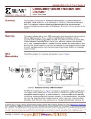
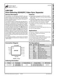
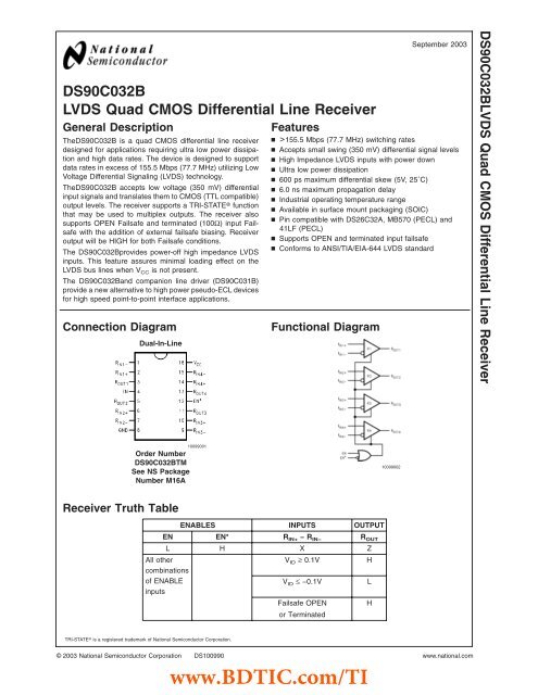
<strong>DS90C032B</strong><strong>LVDS</strong> <strong>Quad</strong> <strong>CMOS</strong> <strong>Differential</strong> <strong>Line</strong> <strong>Receiver</strong>General DescriptionThe<strong>DS90C032B</strong> is a quad <strong>CMOS</strong> differential line receiverdesigned for applications requiring ultra low power dissipationand high data rates. The device is designed to supportdata rates in excess of 155.5 Mbps (77.7 MHz) utilizing LowVoltage <strong>Differential</strong> Signaling (<strong>LVDS</strong>) technology.The<strong>DS90C032B</strong> accepts low voltage (350 mV) differentialinput signals and translates them to <strong>CMOS</strong> (TTL compatible)output levels. The receiver supports a TRI-STATE ® functionthat may be used to multiplex outputs. The receiver alsosupports OPEN Failsafe and terminated (100Ω) input Failsafewith the addition of external failsafe biasing. <strong>Receiver</strong>output will be HIGH for both Failsafe conditions.The <strong>DS90C032B</strong>provides power-off high impedance <strong>LVDS</strong>inputs. This feature assures minimal loading effect on the<strong>LVDS</strong> bus lines when V CC is not present.The <strong>DS90C032B</strong>and companion line driver (DS90C031B)provide a new alternative to high power pseudo-ECL devicesfor high speed point-to-point interface applications.Connection DiagramDual-In-<strong>Line</strong>Featuresn >155.5 Mbps (77.7 MHz) switching ratesn Accepts small swing (350 mV) differential signal levelsn High Impedance <strong>LVDS</strong> inputs with power downn Ultra low power dissipationn 600 ps maximum differential skew (5V, 25˚C)n 6.0 ns maximum propagation delayn Industrial operating temperature rangen Available in surface mount packaging (SOIC)n Pin compatible with DS26C32A, MB570 (PECL) and41LF (PECL)n Supports OPEN and terminated input failsafen Conforms to ANSI/TIA/EIA-644 <strong>LVDS</strong> standardFunctional DiagramSeptember 2003<strong>DS90C032B</strong><strong>LVDS</strong> <strong>Quad</strong> <strong>CMOS</strong> <strong>Differential</strong> <strong>Line</strong> <strong>Receiver</strong>10099001Order Number<strong>DS90C032B</strong>TMSee NS PackageNumber M16A10099002<strong>Receiver</strong> Truth TableENABLES INPUTS OUTPUTEN EN* R IN+ −R IN− R OUTL H X ZAll otherV ID ≥ 0.1VHcombinationsof ENABLEV ID ≤ −0.1VLinputsFailsafe OPENHor TerminatedTRI-STATE ® is a registered trademark of National Semiconductor Corporation.© 2003 National Semiconductor Corporation DS100990 www.national.comwww.BDTIC.com/TI
<strong>DS90C032B</strong>Absolute Maximum Ratings (Note 1)If Military/Aerospace specified devices are required,please contact the National Semiconductor Sales Office/Distributors for availability and specifications.ESD Rating (Note 7)(HBM, 1.5 kΩ, 100 pF)(EIAJ, 0 Ω, 200 pF)≥ 2kV≥ 250VSupply Voltage (V CC ) −0.3V to +6VInput Voltage (R IN+ ,R IN− )−0.3V to +5.8VEnable Input Voltage(EN, EN*)−0.3V to (V CC + 0.3V)Output Voltage (R OUT )−0.3V to (V CC + 0.3V)Maximum Package Power Dissipation @ +25˚CM Package1025 mWDerate M Package8.2 mW/˚C above+25˚CStorage Temperature Range −65˚C to +150˚CLead Temperature RangeSoldering (4 sec.)+260˚CMaximum JunctionTemperature+150˚CRecommended OperatingConditionsSupply Voltage(V CC )<strong>Receiver</strong> InputVoltageMin Typ Max Units+4.5 +5.0 +5.5 VGND 2.4 VOperating Free Air Temperature(T A )<strong>DS90C032B</strong>T −40 +25 +85 ˚CElectrical CharacteristicsOver Supply Voltage and Operating Temperature ranges, unless otherwise specified. (Notes 2, 3)+100 mVSymbol Parameter Conditions Pin Min Typ Max UnitsV TH <strong>Differential</strong> Input High Threshold V CM = +1.2V R IN+ ,V TL <strong>Differential</strong> Input Low Threshold R IN− −100 mVI IN Input Current V IN = +2.4V V CC = 5.5V or 0V −10 ±1 +10 µAV IN = 0V −10 ±1 +10 µAV OH Output High Voltage I OH = −0.4 mA, V ID = +200 mV R OUT 3.8 4.9 VI OH = −0.4 mA, Input terminated 3.8 4.9 VV OL Output Low Voltage I OL = 2 mA, V ID = −200 mV 0.07 0.3 VI OS Output Short Circuit Current Enabled, V OUT = 0V (Note 8) −15 −60 −100 mAI OZ Output TRI-STATE Current Disabled, V OUT =0VorV CC −10 ±1 +10 µAV IH Input High Voltage EN, 2.0 VV IL Input Low Voltage EN*0.8 VI I Input Current −10 ±1 +10 µAV CL Input Clamp Voltage I CL = −18 mA −1.5 −0.8 VI CC No Load Supply Current EN, EN* = V CC or GND, Inputs Open V CC 3.5 10 mA<strong>Receiver</strong>s Enabled EN, EN* = 2.4 or 0.5, Inputs Open 3.7 11 mAI CCZ No Load Supply Current<strong>Receiver</strong>s DisabledEN = GND, EN* = V CC , Inputs Open 3.5 10 mAwww.national.com 2www.BDTIC.com/TI
Switching CharacteristicsV CC = +5.0V, T A = +25˚C (Notes 3, 4, 9)Symbol Parameter Conditions Min Typ Max Unitst PHLD <strong>Differential</strong> Propagation Delay High to Low C L = 5 pF 1.5 3.40 5.0 nst PLHD <strong>Differential</strong> Propagation Delay Low to High V ID = 200 mV 1.5 3.48 5.0 nst SKD <strong>Differential</strong> Skew |t PHLD −t PLHD | (Figure 1 and Figure 2) 0 80 600 pst SK1 Channel-to-Channel Skew (Note 5) 0 0.6 1.0 nst TLH Rise Time 0.5 2.0 nst THL Fall Time 0.5 2.0 nst PHZ Disable Time High to Z R L =2kΩ 10 15 nst PLZ Disable Time Low to Z C L =10pF 10 15 nst PZH Enable Time Z to High (Figure 3 and Figure 4) 4 10 nst PZL Enable Time Z to Low 4 10 ns<strong>DS90C032B</strong>Switching CharacteristicsV CC = +5.0V ± 10%, T A = −40˚C to +85˚C (Notes 3, 4, 9)Symbol Parameter Conditions Min Typ Max Unitst PHLD <strong>Differential</strong> Propagation Delay High to Low C L = 5 pF 1.0 3.40 6.0 nst PLHD <strong>Differential</strong> Propagation Delay Low to High V ID = 200 mV 1.0 3.48 6.0 nst SKD <strong>Differential</strong> Skew |t PHLD −t PLHD | (Figure 1 and Figure 2) 0 0.08 1.2 nst SK1 Channel-to-Channel Skew (Note 5) 0 0.6 1.5 nst SK2 Chip to Chip Skew (Note 6) 5.0 nst TLH Rise Time 0.5 2.5 nst THL Fall Time 0.5 2.5 nst PHZ Disable Time High to Z R L =2kΩ 10 20 nst PLZ Disable Time Low to Z C L =10pF 10 20 nst PZH Enable Time Z to High (Figure 3 and Figure 4) 4 15 nst PZL Enable Time Z to Low 4 15 nsNote 1: “Absolute Maximum Ratings” are those values beyond which the safety of the device cannot be guaranteed. They are not meant to imply that the devicesshould be operated at these limits. The table of “Electrical Characteristics” specifies conditions of device operation.Note 2: Current into device pins is defined as positive. Current out of device pins is defined as negative. All voltages are referenced to ground unless otherwisespecified.Note 3: All typicals are given for: V CC = +5.0V, T A = +25˚C.Note 4: Generator waveform for all tests unless otherwise specified: f=1MHz, Z O =50Ω, t r and t f (0%–100%) ≤ 1 ns for R IN and t r and t f ≤ 6 ns for EN or EN*.Note 5: Channel-to-Channel Skew is defined as the difference between the propagation delay of one channel and that of the others on the same chip with an eventon the inputs.Note 6: Chip to Chip Skew is defined as the difference between the minimum and maximum specified differential propagation delays.Note 7: ESD Rating:HBM (1.5 kΩ, 100 pF) ≥ 2kVEIAJ (0Ω, 200 pF) ≥ 250VNote 8: Output short circuit current (I OS ) is specified as magnitude only, minus sign indicates direction only. Only one output should be shorted at a time, do notexceed maximum junction temperature specification.Note 9: C L includes probe and jig capacitance.Parameter Measurement Information10099003FIGURE 1. <strong>Receiver</strong> Propagation Delay and Transition Time Test Circuit3www.BDTIC.com/TIwww.national.com
<strong>DS90C032B</strong>Parameter Measurement Information (Continued)10099004FIGURE 2. <strong>Receiver</strong> Propagation Delay and Transition Time WaveformsC L includes load and test jig capacitance.S 1 =V CC for t PZL and t PLZ measurements.S 1 = GND for t PZH and t PHZ measurements.10099005FIGURE 3. <strong>Receiver</strong> TRI-STATE Delay Test Circuit10099006FIGURE 4. <strong>Receiver</strong> TRI-STATE Delay Waveformswww.national.com 4www.BDTIC.com/TI
Typical Application<strong>DS90C032B</strong>10099007FIGURE 5. Point-to-Point ApplicationApplications Information<strong>LVDS</strong> drivers and receivers are intended to be primarily usedin an uncomplicated point-to-point configuration as is shownin Figure 5. This configuration provides a clean signalingenvironment for the quick edge rates of the drivers. Thereceiver is connected to the driver through a balanced mediawhich may be a standard twisted pair cable, a parallel paircable, or simply PCB traces. Typically the characteristicimpedance of the media is in the range of 100Ω. A terminationresistor of 100Ω should be selected to match the media,and is located as close to the receiver input pins as possible.The termination resistor converts the current sourced by thedriver into a voltage that is detected by the receiver. Otherconfigurations are possible such as a multi-receiver configuration,but the effects of a mid-stream connector(s), cablestub(s), and other impedance discontinuities as well asground shifting, noise margin limits, and total terminationloading must be taken into account.The<strong>DS90C032B</strong> differential line receiver is capable of detectingsignals as low as 100 mV, over a ±1V common-moderange centered around +1.2V. This is related to the driveroffset voltage which is typically +1.2V. The driven signal iscentered around this voltage and may shift ±1V around thiscenter point. The ±1V shifting may be the result of a groundpotential difference between the driver’s ground referenceand the receiver’s ground reference, the common-mode effectsof coupled noise, or a combination of the two. Bothreceiver input pins should honor their specified operatinginput voltage range of 0V to +2.4V (measured from each pinto ground), exceeding these limits may turn on the ESDprotection circuitry which will clamp the bus voltages.RECEIVER FAILSAFEThe <strong>LVDS</strong> receiver is a high gain, high speed device thatamplifies a small differential signal (20mV) to <strong>CMOS</strong> logiclevels. Due to the high gain and tight threshold of the receiver,care should be taken to prevent noise from appearingas a valid signal.The receiver’s internal failsafe circuitry is designed tosource/sink a small amount of current, providing failsafeprotection (a stable known state of HIGH output voltage) forfloating and terminated (100Ω) receiver inputs in low noiseenvironment (differential noise < 10mV).1. Open Input Pins. The<strong>DS90C032B</strong> is a quad receiverdevice, and if an application requires only 1, 2 or 3receivers, the unused channel(s) inputs should be leftOPEN. Do not tie unused receiver inputs to ground orany other voltages. The input is biased by internal highvalue pull up and pull down resistors to set the output toa HIGH state. This internal circuitry will guarantee aHIGH, stable output state for open inputs.2. Terminated Input. The<strong>DS90C032B</strong> requires externalfailsafe biasing for terminated input failsafe.Terminated input failsafe is the case of a receiver thathas a 100Ω termination across its inputs and the driveris in the following situations. Unplugged from the bus, orthe driver output is in TRI-STATE or in power-off condition.The use of external biasing resistors provide asmall bias to set the differential input voltage while theline is un-driven, and therefore the receiver output will bein HIGH state. If the driver is removed from the bus butthe cable is still present and floating, the unpluggedcable can become a floating antenna that can pick upnoise. The <strong>LVDS</strong> receiver is designed to detect verysmall amplitude and width signals and recover them tostandard logic levels. Thus, if the cable picks up morethan 10mV of differential noise, the receiver may respond.To insure that any noise is seen as commonmodeand not differential, a balanced interconnect andtwisted pair cables is recommended, as they help toensure that noise is coupled common to both lines andrejected by the receivers.3. Operation in environment with greater than 10mVdifferential noise.National recommends external failsafe biasing on its<strong>LVDS</strong> receivers for a number of system level and signalquality reasons. First, only an application that requiresfailsafe biasing needs to employ it. Second, the amountof failsafe biasing is now an application design parameterand can be custom tailored for the specific application.In applications in low noise environments, they maychoose to use a very small bias if any. For applicationswith less balanced interconnects and/or in high noiseenvironments they may choose to boost failsafe further.Nationals "<strong>LVDS</strong> Owner’s Manual provides detailed calculationsfor selecting the proper failsafe biasing resistors.Third, the common-mode voltage is biased by theresistors during the un-driven state. This is selected tobe close to the nominal driver offset voltage (V OS ). Thuswhen switching between driven and un-driven states,the common-mode modulation on the bus is held to aminimum.For additional Failsafe Biasing information, please referto Application Note AN-1194 for more detail.The footprint of the<strong>DS90C032B</strong> is the same as the industrystandard 26LS32 <strong>Quad</strong> <strong>Differential</strong> (RS-422) <strong>Receiver</strong>.For additional <strong>LVDS</strong> application information, please refer toNational’s <strong>LVDS</strong> Owner’s Manual available through National’swebsite www.national.com/appinfo/lvds.5www.BDTIC.com/TIwww.national.com
<strong>DS90C032B</strong>Pin DescriptionsPin No. Name2, 6,10, 141, 7, 9,153, 5,11, 13R IN+R IN−R OUTDescriptionNon-inverting receiver input pinInverting receiver input pin<strong>Receiver</strong> output pin4 EN Active high enable pin, OR-ed withEN*12 EN* Active low enable pin, OR-ed with EN16 V CC Power supply pin, +5V ± 10%8 GND Ground pinOrdering InformationTypical Performance CharacteristicsOperating Package Type/ Order NumberTemperature Number−40˚C to +85˚C SOP/M16A <strong>DS90C032B</strong>TMOutput High Voltage vsPower Supply VoltageOutput High Voltage vsAmbient Temperature10099008 10099009Output Low Voltage vsPower Supply VoltageOutput Low Voltage vsAmbient Temperature10099010 10099011www.national.com 6www.BDTIC.com/TI
Typical Performance Characteristics (Continued)Output Short Circuit Currentvs Power Supply VoltageOutput Short Circuit Currentvs Ambient Temperature<strong>DS90C032B</strong>10099012 10099013<strong>Differential</strong> Propagation Delayvs Power Supply Voltage<strong>Differential</strong> Propagation Delayvs Ambient Temperature10099014 10099015<strong>Differential</strong> Skew vsPower Supply Voltage<strong>Differential</strong> Skew vsAmbient Temperature10099016 100990177www.BDTIC.com/TIwww.national.com
<strong>DS90C032B</strong>Typical Performance Characteristics (Continued)Transition Time vsPower Supply VoltageTransition Time vsAmbient Temperature10099018 10099019www.national.com 8www.BDTIC.com/TI
Physical Dimensions inches (millimeters)unless otherwise noted16-Lead (0.150" Wide) Molded Small Outline Package, JEDECOrder Number <strong>DS90C032B</strong>TMNS Package Number M16A<strong>DS90C032B</strong><strong>LVDS</strong> <strong>Quad</strong> <strong>CMOS</strong> <strong>Differential</strong> <strong>Line</strong> <strong>Receiver</strong>LIFE SUPPORT POLICYNATIONAL’S PRODUCTS ARE NOT AUTHORIZED FOR USE AS CRITICAL COMPONENTS IN LIFE SUPPORTDEVICES OR SYSTEMS WITHOUT THE EXPRESS WRITTEN APPROVAL OF THE PRESIDENT AND GENERALCOUNSEL OF NATIONAL SEMICONDUCTOR CORPORATION. As used herein:1. Life support devices or systems are devices orsystems which, (a) are intended for surgical implantinto the body, or (b) support or sustain life, andwhose failure to perform when properly used inaccordance with instructions for use provided in thelabeling, can be reasonably expected to result in asignificant injury to the user.2. A critical component is any component of a lifesupport device or system whose failure to performcan be reasonably expected to cause the failure ofthe life support device or system, or to affect itssafety or effectiveness.National SemiconductorAmericas CustomerSupport CenterEmail: new.feedback@nsc.comTel: 1-800-272-9959www.national.comNational SemiconductorEurope Customer Support CenterFax: +49 (0) 180-530 85 86Email: europe.support@nsc.comDeutsch Tel: +49 (0) 69 9508 6208English Tel: +44 (0) 870 24 0 2171Français Tel: +33 (0) 1 41 91 8790National SemiconductorAsia Pacific CustomerSupport CenterEmail: ap.support@nsc.comNational SemiconductorJapan Customer Support CenterFax: 81-3-5639-7507Email: jpn.feedback@nsc.comTel: 81-3-5639-7560National does not assume any responsibility for use of any circuitry described, no circuit patent licenses are implied and National reserves the right at any time without notice to change said circuitry and specifications.www.BDTIC.com/TI