Wide range 400W L6599-based HB LLC resonant converter for PDP ...
Wide range 400W L6599-based HB LLC resonant converter for PDP ...
Wide range 400W L6599-based HB LLC resonant converter for PDP ...
- No tags were found...
Create successful ePaper yourself
Turn your PDF publications into a flip-book with our unique Google optimized e-Paper software.
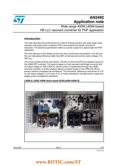
AN2492Application note<strong>Wide</strong> <strong>range</strong> <strong>400W</strong> <strong>L6599</strong>-<strong>based</strong><strong>HB</strong> <strong>LLC</strong> <strong>resonant</strong> <strong>converter</strong> <strong>for</strong> <strong>PDP</strong> applicationIntroductionThis note describes the per<strong>for</strong>mances of a 400 W reference board, with wide-<strong>range</strong> mainsoperation and power-factor-correction (PFC) and presents the results of its benchevaluation. The electrical specification refers to a power supply <strong>for</strong> a typical high-end <strong>PDP</strong>application.The main features of this design are the very low no-load input consumption (
ContentsAN2492Contents1 Main characteristics and circuit description . . . . . . . . . . . . . . . . . . . . . 42 Electrical test results . . . . . . . . . . . . . . . . . . . . . . . . . . . . . . . . . . . . . . . . 92.1 Harmonic content measurement . . . . . . . . . . . . . . . . . . . . . . . . . . . . . . . . 92.2 Efficiency measurements . . . . . . . . . . . . . . . . . . . . . . . . . . . . . . . . . . . . . 102.3 Resonant stage operating wave<strong>for</strong>ms . . . . . . . . . . . . . . . . . . . . . . . . . . . 122.4 Stand-by and no-load power consumption . . . . . . . . . . . . . . . . . . . . . . . . 152.5 Short-circuit protection . . . . . . . . . . . . . . . . . . . . . . . . . . . . . . . . . . . . . . . 162.6 Overvoltage protection . . . . . . . . . . . . . . . . . . . . . . . . . . . . . . . . . . . . . . . 173 Thermal tests . . . . . . . . . . . . . . . . . . . . . . . . . . . . . . . . . . . . . . . . . . . . . . 184 Conducted emission pre-compliance test . . . . . . . . . . . . . . . . . . . . . . 205 Bill of materials . . . . . . . . . . . . . . . . . . . . . . . . . . . . . . . . . . . . . . . . . . . . 226 PFC coil specification . . . . . . . . . . . . . . . . . . . . . . . . . . . . . . . . . . . . . . . 286.1 Electrical characteristics . . . . . . . . . . . . . . . . . . . . . . . . . . . . . . . . . . . . . . 286.2 Mechanical aspect and pin numbering . . . . . . . . . . . . . . . . . . . . . . . . . . . 287 Resonant power trans<strong>for</strong>mer specification . . . . . . . . . . . . . . . . . . . . . 297.1 Electrical characteristics . . . . . . . . . . . . . . . . . . . . . . . . . . . . . . . . . . . . . . 298 Auxiliary flyback power trans<strong>for</strong>mer . . . . . . . . . . . . . . . . . . . . . . . . . . . 318.1 Electrical characteristics . . . . . . . . . . . . . . . . . . . . . . . . . . . . . . . . . . . . . . 319 Board layout . . . . . . . . . . . . . . . . . . . . . . . . . . . . . . . . . . . . . . . . . . . . . . . 3210 References . . . . . . . . . . . . . . . . . . . . . . . . . . . . . . . . . . . . . . . . . . . . . . . . 3411 Revision history . . . . . . . . . . . . . . . . . . . . . . . . . . . . . . . . . . . . . . . . . . . 342/35www.BDTIC.com/ST
AN2492List of figuresList of figuresFigure 1. PFC pre-regulator electrical diagram . . . . . . . . . . . . . . . . . . . . . . . . . . . . . . . . . . . . . . . . . . 6Figure 2. Resonant <strong>converter</strong> electrical diagram . . . . . . . . . . . . . . . . . . . . . . . . . . . . . . . . . . . . . . . . . 7Figure 3. Auxiliary <strong>converter</strong> electrical diagram . . . . . . . . . . . . . . . . . . . . . . . . . . . . . . . . . . . . . . . . . . 8Figure 4. Compliance to EN61000-3-2 <strong>for</strong> harmonic reduction: full load . . . . . . . . . . . . . . . . . . . . . . . 9Figure 5. Compliance to EN EN61000-3-2 <strong>for</strong> harmonic reduction: 70 W load . . . . . . . . . . . . . . . . . . 9Figure 6. Compliance to JEIDA-MITI standard <strong>for</strong> harmonic reduction: full load . . . . . . . . . . . . . . . . . 9Figure 7. Compliance to JEIDA-MITI standard <strong>for</strong> harmonic reduction: 70 W load . . . . . . . . . . . . . . . 9Figure 8. Power factor vs. Vin & load. . . . . . . . . . . . . . . . . . . . . . . . . . . . . . . . . . . . . . . . . . . . . . . . . 10Figure 9. Total harmonic distortion vs. Vin & load . . . . . . . . . . . . . . . . . . . . . . . . . . . . . . . . . . . . . . . 10Figure 10. Overall efficiency versus output power at nominal mains voltages. . . . . . . . . . . . . . . . . . . 10Figure 11. Overall efficiency versus input mains voltage at various output power levels . . . . . . . . . . 12Figure 12. Resonant circuit primary side wave<strong>for</strong>ms at full load . . . . . . . . . . . . . . . . . . . . . . . . . . . . . 13Figure 13. Resonant circuit primary side wave<strong>for</strong>ms at light load (about 30 W output power) . . . . . . 13Figure 14. Resonant circuit primary side wave<strong>for</strong>ms at no load condition. . . . . . . . . . . . . . . . . . . . . . 14Figure 15. Resonant circuit secondary side wave<strong>for</strong>ms: +200 V output . . . . . . . . . . . . . . . . . . . . . . . 14Figure 16. Low frequency (100 Hz) ripple voltage on the +200 V output. . . . . . . . . . . . . . . . . . . . . . . 15Figure 17. Load transition (0.4 A - 2 A) on +200 V output voltage. . . . . . . . . . . . . . . . . . . . . . . . . . . . 15Figure 18. +200 V output short-circuit wave<strong>for</strong>ms . . . . . . . . . . . . . . . . . . . . . . . . . . . . . . . . . . . . . . . . 17Figure 19. Thermal map @115 V AC - full load . . . . . . . . . . . . . . . . . . . . . . . . . . . . . . . . . . . . . . . . . . . 19Figure 20. Thermal map at 230 V AC - full load . . . . . . . . . . . . . . . . . . . . . . . . . . . . . . . . . . . . . . . . . . . 19Figure 21. Peak measurement on LINE at 115 V AC and full load . . . . . . . . . . . . . . . . . . . . . . . . . . . . 20Figure 22. Peak measurement on NEUTRAL at 115 V AC and full load . . . . . . . . . . . . . . . . . . . . . . . . 20Figure 23. Peak measurement on LINE at 230 V AC and full load . . . . . . . . . . . . . . . . . . . . . . . . . . . . 21Figure 24. Peak measurement on NEUTRAL at 230 V AC and full load . . . . . . . . . . . . . . . . . . . . . . . . 21Figure 25. Electrical diagram . . . . . . . . . . . . . . . . . . . . . . . . . . . . . . . . . . . . . . . . . . . . . . . . . . . . . . . . 28Figure 26. Pin side view. . . . . . . . . . . . . . . . . . . . . . . . . . . . . . . . . . . . . . . . . . . . . . . . . . . . . . . . . . . . 29Figure 27. Electrical diagram . . . . . . . . . . . . . . . . . . . . . . . . . . . . . . . . . . . . . . . . . . . . . . . . . . . . . . . . 29Figure 28. Mechanical aspect and pin numbering . . . . . . . . . . . . . . . . . . . . . . . . . . . . . . . . . . . . . . . . 30Figure 29. Winding position on coil <strong>for</strong>mer. . . . . . . . . . . . . . . . . . . . . . . . . . . . . . . . . . . . . . . . . . . . . . 30Figure 30. Electrical diagram . . . . . . . . . . . . . . . . . . . . . . . . . . . . . . . . . . . . . . . . . . . . . . . . . . . . . . . . 31Figure 31. Auxiliary trans<strong>for</strong>mer winding position on coil <strong>for</strong>mer . . . . . . . . . . . . . . . . . . . . . . . . . . . . . 32Figure 32. Copper tracks . . . . . . . . . . . . . . . . . . . . . . . . . . . . . . . . . . . . . . . . . . . . . . . . . . . . . . . . . . . 32Figure 33. Thru-hole component placing and top silk screen . . . . . . . . . . . . . . . . . . . . . . . . . . . . . . . 33Figure 34. SMT component placing and bottom silk screen . . . . . . . . . . . . . . . . . . . . . . . . . . . . . . . . 333/35www.BDTIC.com/ST
Main characteristics and circuit descriptionAN24921 Main characteristics and circuit descriptionThe main characteristics of the SMPS are listed below:●●●●●●●●Universal input mains <strong>range</strong>: 90 to 264 V AC - 45 to 65 HzOutput voltages: 200 V @ 2 A - 3.3 V @ 0.7 A - 5 V @ 1 AMains harmonics: Compliance with EN61000-3-2 specificationsStand-by mains consumption: Typical 0.5 W @230 V ACOverall efficiency: better than 88% at full load, 90-264 V ACEMI: Compliance with EN55022-class B specificationsSafety: Compliance with EN60950 specificationsPCB single layer: 132x265 mm, mixed PTH/SMT technologiesThe circuit consists of three stages. A front-end PFC pre-regulator implemented by thecontroller L6563 (Figure 1), a half-bridge <strong>resonant</strong> DC/DC <strong>converter</strong> <strong>based</strong> on the <strong>resonant</strong>controller <strong>L6599</strong> (Figure 2) and a 7 W flyback <strong>converter</strong> intended <strong>for</strong> stand-by management(Figure 3) utilizing the VIPer12A off-line primary switcher.The PFC stage delivers a stable 400 VDC supply to the downstream <strong>converter</strong>s (<strong>resonant</strong> +flyback) and provides <strong>for</strong> the reduction of the current harmonics drawn from the mains, inorder to meet the requirements of the European norm EN61000-3-2 and the JEIDA-MITInorm <strong>for</strong> Japan.The PFC controller is the L6563 (U1), integrating all functions needed to operate the PFCand interface the downstream <strong>resonant</strong> <strong>converter</strong>. Though this controller chip is designed <strong>for</strong>Transition-Mode (TM) operation, where the boost inductor works next to the boundarybetween Continuous (CCM) and Discontinuous Conduction Mode (DCM), by adding asimple external circuit, it can be operated in LM-FOT (line-modulated fixed off-time) mode,allowing Continuous Conduction Mode operation, normally achievable with more expensivecontrol chips and more complex architectures. This operative mode allows the use of thisdevice at a high power level, usually covered by CCM topologies. For a detailed andcomplete description of the LM-FOT operating mode, see the application note AN1792. Theexternal components to configure the circuit in LM-FOT mode are: C15, C17, D5, Q3, R14,R17 and R29.The power stage of the PFC is a conventional boost <strong>converter</strong>, connected to the output ofthe rectifier bridge through a differential mode filtering cell (C5, C6 and L3) <strong>for</strong> EMIreduction. It includes a coil (L4), a diode (D3), and two capacitors (C7 and C8). The boostswitch consists of two Power MOSFETs (Q1 and Q2), connected in parallel, which aredirectly driven by the L6563 output drive thanks to the high current capability of the IC. Thedivider (R30, R31 and R32) connected to MULT pin 3 brings the in<strong>for</strong>mation of theinstantaneous voltage that is used to modulate the boost current and to derive furtherin<strong>for</strong>mation like the average value of the AC line used by the VFF (voltage feed-<strong>for</strong>ward)function. This function is used to keep the output voltage almost independent of the mains.The divider (R3, R6, R8, R10 and R11) is dedicated to detecting the output voltage while afurther divider (R5, R7, R9, R16 and R25) is used to protect the circuit in case of voltageloop failure.The second stage is an <strong>LLC</strong> <strong>resonant</strong> <strong>converter</strong>, with half-bridge topology implementation,working in ZVS (zero voltage switching) mode. The controller is the <strong>L6599</strong> integrated circuitthat incorporates the necessary functions to properly drive the two half-bridge MOSFETs bya 50% fixed duty cycle with fixed dead-time, changing the frequency according to the4/35www.BDTIC.com/ST
AN2492Main characteristics and circuit descriptionfeedback signal in order to regulate the output voltages against load and input voltagevariations.The main features of the <strong>L6599</strong> are a non-linear soft-start, a current protection mode usedto program the hiccup mode timing, a dedicated pin <strong>for</strong> sequencing or brown-out (LINE) anda stand-by pin (STBY) <strong>for</strong> burst mode operation at light loads (not used in this design).The trans<strong>for</strong>mer (T1) uses the magnetic integration approach, incorporating the <strong>resonant</strong>series and shunt inductances of the <strong>LLC</strong> <strong>resonant</strong> tank. Thus, no additional external coilsare needed <strong>for</strong> the resonance. For a detailed analysis of the <strong>LLC</strong> <strong>resonant</strong> <strong>converter</strong>, pleaserefer to the application note AN2450.The secondary side power circuit is configured with a single-ended trans<strong>for</strong>mer winding andfull-bridge rectification (diodes D8A, D8B, D10A, D10B), which is more suitable <strong>for</strong> thecurrent design. In fact, with this configuration, the total junction capacitance of the outputdiodes reflected at primary side is one half the capacitance in case of center-taptrans<strong>for</strong>mer. This capacitance at trans<strong>for</strong>mer primary side may affect the behavior of the<strong>resonant</strong> tank, changing the circuit from <strong>LLC</strong> to <strong>LLC</strong>C type, with the risk that the <strong>converter</strong>,in light-load/no-load condition (when the feedback loop increases the operating frequency)can no longer control the output voltage. If the <strong>converter</strong> has to operate down to zero load,this capacitance needs to be minimized. An inherent advantage of the full-bridgerectification is that the voltage rating of the output diodes in this configuration is one half therating necessary <strong>for</strong> center-tap and two diodes circuit, which translates into a lower junctioncapacitance device, with consequent lower reflected capacitance at primary side.The feedback loop is implemented by means of a classical configuration using a TL431 (U4)to adjust the current in the optocoupler diode (U3). The optocoupler transistor modulates thecurrent from controller Pin 4, so the frequency will change accordingly, thus achieving theoutput voltage regulation. Resistors R46 and R54 set the maximum operating frequency. Incase of a short circuit, the current entering the primary winding is detected by the losslesscircuit (C34, C39, D11, D12, R43, and R45) and the resulting signal is fed into <strong>L6599</strong> Pin 6.In case of overload, the voltage on Pin 6 will exceed an internal threshold that triggers aprotection sequence via Pin 2, keeping the current flowing in the circuit at a safe level.The third stage is a small flyback <strong>converter</strong> <strong>based</strong> on the VIPer12A, a current modecontroller with integrated Power MOSFET, capable of delivering about 7 W total outputpower on the output voltages (5 V and 3.3 V). The regulated output voltage is the 3.3 Voutput and, also in this case, the feedback loop uses the TL431 (U7) and optocoupler (U6)to control the output voltage. This <strong>converter</strong> is able to operate in the whole mains voltage<strong>range</strong>, even when the PFC stage is not working. From the auxiliary winding on the primaryside of the flyback trans<strong>for</strong>mer (T2), a voltage Vs is available, intended to supply the othercontrollers (L6563 and <strong>L6599</strong>) in addition to the VIPer12A itself.The PFC stage and the <strong>resonant</strong> <strong>converter</strong> can be switched on and off through the circuit<strong>based</strong> mainly on components Q7, Q8, D22 and U8, which, depending on the level of thesignal ST-BY, supplies or removes the auxiliary voltage (VAUX) necessary to start up thecontrollers of the PFC and <strong>resonant</strong> stages. When the AC input voltage is applied to thepower supply, the small flyback <strong>converter</strong> switches on first. Then, when the ST-BY signal islow, the PFC pre-regulator becomes operative, and the <strong>resonant</strong> <strong>converter</strong> can deliver theoutput power to the load. Note that if Pin 9 of Connector J3 is left floating (no signal ST-BYpresent), the PFC and <strong>resonant</strong> <strong>converter</strong> will not operate, and only +5 V and +3.3 Vsupplies are available on the output. In order to enable the +200 V output, Pin 9 ofConnector J3 must be pulled down to ground.5/35www.BDTIC.com/ST
Main characteristics and circuit descriptionAN24926/35Figure 1.PFC pre-regulator electrical diagramL1CM-1.5mH-5A+-~~D2D15XB60Q1STP12NM50FPC112nF2-Y2C102nF2-Y2C4680nF-X2C3330nF-X2C2470nF-X2C5470nF/630VC6470nF/630VQ2STP12NM50FPR11M5L3DM-51uH-6AD3STTH8R06D11N5406R2NTC 2R5-S237C7470nF/630VC8330uF/450VR240R39R230R39R220R39F18A/250VVdcINVCOMPMULTCSVFFTBOPFC-OK PWM-LATCHPWM-STOPRUNZCDGNDGDVCCU1L6563+400VVrect1-212J1CON2-INC92nF2-Y15-6R186R8R156R8D6LL4148D4LL4148L4PQ40-500uHD5LL4148R1715kR143k3C17220pFC15100pFC18330pFR191k0CSCSR28240kC20470nFC14100nFC161uFR1356kR291k5R6680kR8680kR1115kR10100kR201k0L2CM-10mH-5AVdcR26150kC212nF2R30620kR31620kR3210kC2210nFVrectQ3BC857CC1310uF/50VC12100nFR72M2R52M2C1910nFR2530kR165k1PWM-LatchR92M2R3680kR447LINEVauxR210R39www.BDTIC.com/ST
AN2492Main characteristics and circuit description7/35Figure 2.Resonant <strong>converter</strong> electrical diagramC32100nFC3110uF/50VR3847R4710kC4010nF+200VC5947nFR51330kC60470nFPWM-LatchR461k5R4210 C334nF7R86470RR541k5R87220RLINEVaux12345678J2CON8R561k0R591k0R523k3R6012kR612k2R5375kU4TL431C4447nFD13C-12VC4110uF/50VR85120kC37100uF/250VC38100uF/250VR343k9U3ASFH617A-2U3BSFH617A-2T1T-RES-ER49R50330kR49330kC234uF7R48330kC24470nFC26270pFR371M0R4116kQ5STP14NK50ZC2847nF/630VQ6STP14NK50ZD10ASTTH803D8ASTTH803D8BSTTH803VdcC2522uF/250VC29100uF/250VC30100uF/250VL510uHD10BSTTH803R43150C34220pF/630VD11LL4148D12LL4148C391uF0R4575RR5875kD7LL4148D9LL4148R390RR4047R330RR3547CSSDELAYCFRFMINSTBYISENLINE GNDLVGVCCNCOUTHVGVBOOTDIS PFC-STOPU2<strong>L6599</strong>R360RC27 100nFwww.BDTIC.com/ST
Main characteristics and circuit descriptionAN24928/35Figure 3.Auxiliary <strong>converter</strong> electrical diagramQ10BC847CC54100nFU7TL431C532nF2U6ASFH617A-2U6BSFH617A-2Vs+200VR671k0SSFBVdd DDDDU5VIPER-12AR792k2D151N5822D161N5821D20BAV103C56100nFC451000uF/10VC471000uF/10VC5010uF/50VC46100uF/10VC49100uF/10VQ9BC857CC4810uF/50VR76150kU8ASFH617A-2R75150kU8BSFH617A-2R7410kR774k7D19C-30VSt-ByD18B-10V12345678910J3CON10R690RVdcC5247nFR6822kC51100nFR7110kQ8BC847CR7210kC5510uF/50VR661k0T2T-FLY -AUX-E20+400VR7022RVdc+400VR831M0R84150kC5810nFQ11BC557C+5Vst-byR8030k+3V3+5Vst-byQ7BC547CD22C-15VL733uHL833uHD17LL4148D21B-15VR6247R641k6C571nF0VsVaux+5Vst-byD14PKC-136St-ByR738k2www.BDTIC.com/ST
AN2492Electrical test results2 Electrical test results2.1 Harmonic content measurementThe current harmonics drawn from the mains have been measured according to theEuropean rule EN61000-3-2 Class-D and Japanese rule JEIDA-MITI Class-D, at full loadand 70 W output power, at both nominal input voltages (230 V AC and 100 V AC ). The picturesin Figure 4., Figure 5., Figure 6. and Figure 7. show that the measured current harmonicsare well below the limits imposed by the regulations, both at full load and at 70 W load.Figure 4.Compliance to EN61000-3-2 <strong>for</strong>harmonic reduction: full loadFigure 5.Compliance to EN EN61000-3-2 <strong>for</strong>harmonic reduction: 70 W loadMeasurements @ 230Vac Full loadEN61000-3-2 class D limit sMeasurement s @ 230Vac 70WEN61000-3-2 class D limit s10110.10.10.010.010.0010.0010.00011 2 3 4 5 6 7 8 9 10 11 12 13 14 15 16 17 18 19 200.00011 2 3 4 5 6 7 8 9 10 11 12 13 14 15 16 17 18 19 20Harmonic Order ( n)Harmonic Order ( n)Figure 6.Compliance to JEIDA-MITI standard<strong>for</strong> harmonic reduction: full loadFigure 7.Compliance to JEIDA-MITI standard<strong>for</strong> harmonic reduction: 70 W loadMeasurement s @ 100Vac Full loadJEIDA-MITI class D limitsMeasurement s @ 100Vac 70WJEIDA-MITI class D limits10110.10.10.010.010.0010.0010.00011 2 3 4 5 6 7 8 9 10 11 12 13 14 15 16 17 18 19 200.00011 2 3 4 5 6 7 8 9 10 11 12 13 14 15 16 17 18 19 20Harmonic Order ( n)Harmonic Order ( n)The Power Factor (PF) and the Total Harmonic Distortion (THD) are reported in Figure 8.and Figure 9. It is evident from the picture that the PF stays close to unity in the whole mainsvoltage <strong>range</strong> at full load and at half load, while it decreases at high mains at low load(70W). The THD has similar behavior, remaining within 25% overall the mains voltage <strong>range</strong>and increasing at low load (70 W) at high mains voltage.9/35www.BDTIC.com/ST
Electrical test resultsAN2492Figure 8. Power factor vs. Vin & load Figure 9. Total harmonic distortion vs. Vin &load1.00PFTHD [%]35.000.980.950.930.900.88<strong>400W</strong>200W70W30.0025.0020.0015.0010.005.00<strong>400W</strong>200W70W0.8580 120 160 200 240 280Vin [Vrms]0.0080 120 160 200 240 280Vin [Vrms]2.2 Efficiency measurementsTable 1. and Table 2. show the output voltage measurements at the nominal mains voltagesof 115 V AC and 230 V AC , with different load conditions. For all measurements, both at fullload and at light load operations, the input power is measured using a Yokogawa WT-210digital power meter. Particular attention has to be paid when measuring input power at fullload in order to avoid measurement errors due to the voltage drop on cables andconnections.Figure 10. shows the overall circuit efficiency, measured at each load condition, at bothnominal input mains voltages of 115 V AC and 230 V AC . The values were measured after 30minutes of warm-up at maximum load. The high efficiency of the PFC pre-regulator workingin FOT mode and the very high efficiency of the <strong>resonant</strong> stage working in ZVS (i.e. withnegligible switching losses), provides <strong>for</strong> an overall efficiency better than 88% at full load inthe complete mains voltage <strong>range</strong>. This is a significant high value <strong>for</strong> a two-stage <strong>converter</strong>,especially at low input mains voltage where PFC conduction losses increase. Even at lowerloads, the efficiency still remains high.Figure 10.Overall efficiency versus output power at nominal mains voltages@230Vac@115Vac100%95%90%85%Eff. (%)80%75%70%65%60%0 50 100 150 200 250 300 350 400 450Output Power (W)10/35www.BDTIC.com/ST
AN2492Electrical test resultsThe global efficiency at full load has been measured even at the limits of the input voltage<strong>range</strong>, with good results:At VIN = 90 V AC - full load, the efficiency is 88.48%At VIN = 264 V AC - full load, the efficiency is 93.70%Also at light load, at an output power of about 10% of the maximum level, the overallefficiency is very good, reaching a value better than 79% over the entire input mains voltage<strong>range</strong>. Figure 11. shows the efficiency measured at various output power levels versus inputmains voltage.Table 1. Efficiency measurements @V IN = 115 V AC+200 V@load(A) +5 V @load(A) +3.3 V @load(A) POUT(W) PIN(W) Efficiency202.50 1.989 4.84 0.968 3.33 0.695 409.77 451.38 90.78%202.50 1.751 4.84 0.968 3.33 0.695 361.58 397.70 90.92%202.50 1.501 4.84 0.968 3.33 0.695 310.95 341.39 91.08%202.50 1.251 4.84 0.968 3.33 0.695 260.33 285.86 91.07%202.50 1.000 4.84 0.968 3.33 0.695 209.50 230.96 90.71%202.53 0.751 4.84 0.968 3.33 0.695 159.10 176.63 90.08%202.53 0.500 4.84 0.968 3.33 0.695 108.26 122.62 88.29%202.53 0.250 4.84 0.968 3.33 0.695 57.63 69.04 83.48%202.56 0.150 4.84 0.293 3.33 0.309 32.83 41.14 79.80%202.67 0.051 4.84 0.293 3.33 0.309 12.78 20.34 62.85%Table 2. Efficiency measurements @V IN = 230 V AC+200 V@load(A) +5 V @load(A) +3.3 V @load(A) POUT(W) PIN(W) Efficiency202.50 1.987 4.84 0.968 3.33 0.695 409.37 437.79 93.51%202.50 1.750 4.84 0.968 3.33 0.695 361.37 386.90 93.40%202.50 1.500 4.84 0.968 3.33 0.695 310.75 333.33 93.23%202.50 1.250 4.84 0.968 3.33 0.695 260.12 279.65 93.02%202.50 1.000 4.84 0.968 3.33 0.695 209.50 226.68 92.42%202.50 0.750 4.84 0.968 3.33 0.695 158.87 174.10 91.25%202.53 0.500 4.84 0.968 3.33 0.695 108.26 121.54 89.08%202.53 0.250 4.84 0.968 3.33 0.695 57.63 68.96 83.57%202.54 0.150 4.84 0.293 3.33 0.309 32.83 41.80 78.54%202.67 0.050 4.84 0.293 3.33 0.309 12.58 19.86 63.35%11/35www.BDTIC.com/ST
Electrical test resultsAN2492Figure 11.Overall efficiency versus input mains voltage at various output powerlevels<strong>400W</strong> 200W 70WEff[%]94%93%92%91%90%89%88%87%86%85%80 120 160 200 240 280Vin [Vrms]2.3 Resonant stage operating wave<strong>for</strong>msFigure 12. shows some wave<strong>for</strong>ms during steady state operation of the <strong>resonant</strong> circuit atfull load. The Ch1 wave<strong>for</strong>m is the half-bridge square voltage on Pin 14 of <strong>L6599</strong>, driving the<strong>resonant</strong> circuit. In the picture it is not evident, but the switching frequency is normallyslightly modulated following the PFC pre-regulator 100-Hz ripple that is rejected by the<strong>resonant</strong> control circuitry. The Ch2 wave<strong>for</strong>m represents the trans<strong>for</strong>mer primary currentflowing into the <strong>resonant</strong> tank. As shown, it has almost a sinusoidal shape. The <strong>resonant</strong>tank has been designed (following the procedure presented in the application note AN2450)to operate at a resonance frequency of about 120 kHz when the dc input voltage of the halfbridgecircuit is at 390 V (that is the nominal output voltage of the PFC stage).The <strong>resonant</strong> frequency has been selected at approximately 120 kHz in order to have agood trade off between trans<strong>for</strong>mer losses and dimensions.The <strong>resonant</strong> tank circuit has been designed in order to have a good margin <strong>for</strong> ZVSoperation, providing good efficiency, while the almost sinusoidal current wave<strong>for</strong>m allows <strong>for</strong>an extremely low EMI generation.Figure 13. and Figure 14. shows the same wave<strong>for</strong>ms as Figure 12, when the +200 V outputis at a light load (about 30 W) or not loaded at all. These two graphics demonstrate theability of the <strong>converter</strong> to operate down to zero load, with the output voltage still within theregulation <strong>range</strong>. The <strong>resonant</strong> tank current has a triangular shape and represents themagnetizing current flowing into the trans<strong>for</strong>mer primary side. The oscillation superimposedon the tank current depends on the occurrence of a further resonance due to the parallel ofthe inductances at primary side (the series and shunt inductances in the APR (all primaryreferred) trans<strong>for</strong>mer model presented in AN2450) and the undesired secondary sidecapacitance reflected at the trans<strong>for</strong>mer primary side.12/35www.BDTIC.com/ST
AN2492Electrical test resultsFigure 12.Resonant circuit primary side wave<strong>for</strong>ms at full loadCh1: half-bridge squarevoltage on pin 14 of <strong>L6599</strong>Ch2: <strong>resonant</strong> tank currentCh3: low side MOSFETdrive signalFigure 13.Resonant circuit primary side wave<strong>for</strong>ms at light load (about 30 W outputpower)Ch1: half-bridge squarevoltage on pin 14 of <strong>L6599</strong>Ch2: <strong>resonant</strong> tank currentCh3: low side MOSFETdrive signal13/35www.BDTIC.com/ST
Electrical test resultsAN2492Figure 14.Resonant circuit primary side wave<strong>for</strong>ms at no load conditionCh1: half-bridge squarevoltage on pin 14 of <strong>L6599</strong>Ch2: <strong>resonant</strong> tank currentCh3: low side MOSFETdrive signalIn Figure 15., wave<strong>for</strong>ms relevant to the secondary side are represented. In particular, thewave<strong>for</strong>m Ch1 is the voltage of D8A anode referenced to the secondary ground potential,while the wave<strong>for</strong>m CH3 shows the current flowing into D8A-D10B diodes. Also this currentwave<strong>for</strong>m (like the one flowing into the <strong>resonant</strong> tank at the trans<strong>for</strong>mer primary side) hasalmost a sine shape, and its average value is one half the output average current.Thanks to the advantages of the <strong>resonant</strong> <strong>converter</strong>, the high frequency noise on the outputvoltages is less than 50 mV, while the residual ripple at twice the mains frequency (100 Hz)is about 150 mV at maximum load and worse line condition (90 V AC ), as shown in Figure 16.Figure 15.Resonant circuit secondary side wave<strong>for</strong>ms: +200 V outputCh1: anode voltage of diode D8ACh2: current into diode D8A14/35www.BDTIC.com/ST
AN2492Electrical test resultsFigure 16.Low frequency (100 Hz) ripple voltage on the +200 V outputCh2: <strong>resonant</strong> tank currentenvelopeCh3: +200 V output voltageripple at 100 HzFigure 17. shows the dynamic behavior of the <strong>converter</strong> during a load variation from 20% to100% on the +200 V output. This figure also highlights the induced effect of this load changeon the PFC pre-regulator output voltage (+400 V on Ch1 track). Both the transitions (from20% to 100% and from 100% to 20%) are clean and do not show any problem <strong>for</strong> the outputvoltage regulation.This shows that the proposed architecture is also highly suitable <strong>for</strong> power suppliesoperating with strong load variation without any problems related to the load regulation.Figure 17.Load transition (0.4 A - 2 A) on +200 V output voltageCh1: PFC output voltageCh2: <strong>resonant</strong> tank currentenvelopeCh3: +200 V output voltageripple2.4 Stand-by and no-load power consumptionThe board is specifically designed <strong>for</strong> light load and zero load operations, typical conditionsoccurring during Stand-by or Power-off operations, when no power is requested from the15/35www.BDTIC.com/ST
Electrical test resultsAN2492+200 V output. Though the <strong>resonant</strong> <strong>converter</strong> can operate down to zero load, some actionsare required to keep the input power drawn from the mains very low when the completesystem is in this load condition. Thus, when entering this power management mode, the ST-BY signal needs to be set high (by the microcontroller of the system). This <strong>for</strong>ces the PFCpre-regulator and the <strong>resonant</strong> stage to switch off, because the supply voltage of the twocontrol ICs is no longer present (Figure 3) and only the auxiliary flyback <strong>converter</strong> continuesworking just to supply the microprocessor circuitry.Table 3. and Table 4. show the measurements of the input power in several light loadconditions at 115 and 230 V AC . These tables show that at no-load the input power is about0.5 W.Table 3. Stand-by consumption at VIN = 115 V AC+5 V @load(A) +3.3 V @load(A) POUT(W) PIN(W)5.06 - 0.017 3.33 - 0.102 0.425 0.8605.04 - 0.017 3.33 - 0.079 0.349 0.7504.98 - 0.017 3.33 - 0.046 0.238 0.5814.90 - 0.017 3.33 - 0.024 0.163 0.4754.47 - 0.000 3.33 - 0.000 0.00 0.245Table 4. Stand-by consumption at VIN = 230 V AC+5 V @load(A) +3.3 V @load(A) POUT(W) PIN(W)5.06 - 0.017 3.33 - 0.102 0.425 1.1565.04 - 0.017 3.33 - 0.079 0.349 1.0444.98 - 0.017 3.33 - 0.046 0.238 0.8704.90 - 0.017 3.33 - 0.024 0.163 0.7554.47 - 0.000 3.33 - 0.000 0.00 0.5102.5 Short-circuit protectionThe <strong>L6599</strong> is equipped with a current sensing input (pin 6, ISEN) and a dedicatedovercurrent management system. The current flowing in the circuit is detected (through thenot dissipative sensing circuit already mentioned in Chapter 1, mainly <strong>based</strong> on a capacitivedivider <strong>for</strong>med by the <strong>resonant</strong> capacitor C28 and the capacitor C34, followed by anintegration cell D12, R45, C39) and the signal is fed into the ISEN pin. This is internallyconnected to the input of a first comparator, referenced to 0.8 V, and to that of a secondcomparator referenced to 1.5 V. If the voltage externally applied to the ISEN pin exceeds 0.8V, the first comparator is tripped causing an internal switch to be turned on discharging thesoft-start capacitor CSS.For output short-circuits, this operation results in a nearly constant peak primary current.The designer can externally program the maximum time (t SH ) that the <strong>converter</strong> is allowedto run overloaded or under short-circuit conditions. Overloads or shortcircuits lasting lessthan t SH will not cause any other action, hence providing the system with immunity to shortduration phenomena. If, instead, t SH is exceeded, an overload protection (OLP) procedure is16/35www.BDTIC.com/ST
AN2492Electrical test resultsactivated that shuts down the device and, in case of continuous overload/short circuit,results in continuous intermittent operation with a user-defined duty cycle. This function isaccomplished by the DELAY pin 2 of the <strong>resonant</strong> controller, by means of the capacitor C24and the parallel resistor R37 connected to ground. As the voltage on the ISEN pin exceeds0.8V, the first OCP comparator, in addition to discharging CSS, turns on an internal currentgenerator that via the DELAY pin charges C24. As the voltage on C24 reaches 3.5 V, the<strong>L6599</strong> stops switching and the internal generator is turned off, so that C24 will now be slowlydischarged by R37. The IC will restart when the voltage on C24 becomes less than 0.3 V.Additionally, if the voltage on the ISEN pin reaches 1.5 V <strong>for</strong> any reason (e.g. trans<strong>for</strong>mersaturation), the second comparator will be triggered, the device will shut down and theoperation will be resumed after an on-off cycle. Figure 18. illustrates the short-circuitprotection sequence described above. The on-off operation is controlled by the voltage onpin 2 (DELAY), providing <strong>for</strong> the hiccup mode of the circuit. Thanks to this control pin, thedesigner can select the hiccup mode timing and thus keep the average output current at asafe level.Figure 18.+200 V output short-circuit wave<strong>for</strong>msCh1: half-bridge voltage on pin14Ch2: + 200 V output currentCh3: pin 6 (ISEN)Ch4: pin 2 (DELAY)2.6 Overvoltage protectionBoth the PFC pre-regulator and the <strong>resonant</strong> <strong>converter</strong> are equipped with their ownovervoltage protection circuit. The PFC controller is internally equipped with a dynamic anda static overvoltage protection circuit sensing the current flowing through the error amplifiercompensation network and entering in the COMP pin (#2). When this current reaches about18 µA, the output voltage of the multiplier is <strong>for</strong>ced to decrease, thus reducing the energydrawn from the mains. If the current exceeds 20 µA, the OVP is triggered (Dynamic OVP),and the external power transistor is switched off until the current falls approximately below 5µA. However, if the overvoltage persists (e.g. in case the load is completely disconnected),the error amplifier will eventually saturate low, triggering an internal comparator (Static OVP)that will keep the external power switch turned off until the output voltage comes back closeto the regulated value. Moreover, in the L6563 there is additional protection against loopfailures using an additional divider (R5, R7, R9, R16 and R25) connected to a dedicated pin(PFC_OK, Pin 7) protecting the circuit in case of loop failures, disconnection, or deviationfrom the nominal value of the feedback loop divider. Hence the PFC output voltage is always17/35www.BDTIC.com/ST
Thermal testsAN2492under control and if a fault condition is detected, the PFC_OK circuitry will latch the PFCoperation and, by means of the PWM_LATCH pin 8 it will also latch the <strong>L6599</strong> via the DISpin of the <strong>resonant</strong> controller.The OVP circuit (see Figure 3) <strong>for</strong> the output voltages of the <strong>resonant</strong> <strong>converter</strong> uses aresistive divider (R75, R76, R80) and the zener diode D21 to sense the +200 V output: if thesensed voltage exceeds the threshold imposed by the zener diode plus the VBE of Q10, thetransistor Q9 starts conducting and the optocoupler U8 opens Q7, so that the VAUX supplyvoltage of the controller ICs L6563 and <strong>L6599</strong> is no longer available. This state is latcheduntil a mains voltage recycle occurs.3 Thermal testsIn order to check design reliability, a thermal mapping by an IR Camera was per<strong>for</strong>med.Figure 19. and Figure 20. show the thermal measurements of the board, component side, atnominal input voltage. The correlation between measurement points and components isindicated <strong>for</strong> both diagrams in Table 5.All other board components work well within the temperature limits, assuring a reliable longterm operation of the power supply.Note that the temperatures of L4 and T1 have been measured both on the ferrite core (Fe)and on the copper winding (Cu).Table 5.Key components temperature at nominal voltages and full loadPoint Item 230 V AC 115 V ACA D2 40,3°C 47,6°CB L4-(FE) 44,2°C 50,5°CC L4-(CU) 46,0°C 55,5°CD Q1 44,5°C 53,4°CE R2 63,5°C 73,0°CF D3 46,1°C 51,0°CG C8 39,3°C 40,1°CH Q6 51,4°C 52,8°CI T1-(CU) 63,7°C 62,6°CJ T1-(FE) 51,3°C 49,6°CK U5 53,2°C 53,4°CL D14 51,8°C 52,3°CM C38 39,4°C 38,5°CN C45 36,1°C 35,7°CO D8A 44,5°C 44,9°CP R22 41,4°C 55,6°C18/35www.BDTIC.com/ST
AN2492Thermal testsTable 5.Key components temperature at nominal voltages and full loadPoint Item 230 V AC 115 V ACQ D15 43,3°C 43,5°CR D16 42,6°C 42,1°CS T2 43,3°C 43,6°CFigure 19.Thermal map @115 V AC - full loadFigure 20.Thermal map at 230 V AC - full load19/35www.BDTIC.com/ST
Conducted emission pre-compliance testAN24924 Conducted emission pre-compliance testThe measurements have been taken in peak detection mode, both on LINE and on Neutralat nominal input mains and at full load. The limits indicated on the following diagrams referto the EN55022 Class- B specifications (the higher limit curve is the quasi-peak limit whilethe lower curve is the average limit) and the measurements show that the PSU emission iswell below the maximum allowed limit.Figure 21.Peak measurement on LINE at 115 V AC and full loadFigure 22.Peak measurement on NEUTRAL at 115 V AC and full load20/35www.BDTIC.com/ST
AN2492Conducted emission pre-compliance testFigure 23.Peak measurement on LINE at 230 V AC and full loadFigure 24.Peak measurement on NEUTRAL at 230 V AC and full load21/35www.BDTIC.com/ST
Bill of materialsAN24925 Bill of materialsTable 6. Bill of materialsItem Part Description SupplierC2 470 nF-X2 275 V AC X2 SAFETY CAPACITOR MKP R46 ARCOTRONICSC3 330 nF-X2 275 V AC X2 SAFETY CAPACITOR MKP R46 ARCOTRONICSC4 680 nF-X2 27 5 V AC X2 SAFETY CAPACITOR MKP R46 ARCOTRONICSC5 470 nF/630 V POLYPROPYLENE CAPACITOR HIGH RIPPLE MKP R71 ARCOTRONICS - EPCOSC6 470 nF/630 V POLYPROPYLENE CAPACITOR HIGH RIPPLE MKP R71 ARCOTRONICS - EPCOSC7 470 nF/630 V POLYPROPYLENE CAPACITOR HIGH RIPPLE MKP R71 ARCOTRONICS - EPCOSC8 330 µF/450 V ALUMINIUM ELCAP USC SERIES 85 DEG SNAP-IN RUBYCONC9 2 nF2-Y1 400 V AC Y1 SAFETY CERAMIC DISK CAPACITOR MURATAC10 2 nF2-Y1 250 V AC Y1 SAFETY CERAMIC DISK CAPACITOR MURATAC11 2 nF2-Y1 250 V AC Y1 SAFETY CERAMIC DISK CAPACITOR MURATAC12 100 nF 50 V 1206 SMD CERCAP GENERAL PURPOSE AVXC13 10 µF/50 V ALUMINIUM ELCAP GENERAL PURPOSE 85 DEG RUBYCONC14 100 nF 50 V 1206 SMD CERCAP GENERAL PURPOSE AVXC15 100 pF 100 V 0805 SMD CERCAP GENERAL PURPOSE AVXC16 1 µF 25 V 1206 SMD CERCAP GENERAL PURPOSE AVXC17 220 pF 100 V 0805 SMD CERCAP GENERAL PURPOSE AVXC18 330 pF 100 V 0805 SMD CERCAP GENERAL PURPOSE AVXC19 10 nF 100 V 0805 SMD CERCAP GENERAL PURPOSE AVXC20 470 nF 50 V 1206 SMD CERCAP GENERAL PURPOSE AVXC21 2 nF2 100 V 1206 SMD CERCAP GENERAL PURPOSE AVXC22 10 nF 100 V 0805 SMD CERCAP GENERAL PURPOSE AVXC23 4 µF7 16 V 1206 SMD CERCAP GENERAL PURPOSE AVXC24 470 nF 25 V 1206 SMD CERCAP GENERAL PURPOSE AVXC25 22 µF/250 V ALUMINIUM ELCAP YXF SERIES 105 DEG RUBYCONC26 270 pF 100 V 0805 SMD CERCAP GENERAL PURPOSE AVXC27 100 nF 50 V 1206 SMD CERCAP GENERAL PURPOSE AVXC28 47 nF/630 V POLYPROPYLENE CAPACITOR HIGH RIPPLE PHE450 RIFA-EVOXC29 100 µF/250 V ALUMINIUM ELCAP YXF SERIES 105 DEG RUBYCONC30 100 µF/250 V ALUMINIUM ELCAP YXF SERIES 105 DEG RUBYCONC31 10 µF/50 V ALUMINIUM ELCAP GENERAL PURPOSE 85 DEG RUBYCONC32 100 nF 50 V 1206 SMD CERCAP GENERAL PURPOSE AVXC33 4 nF7 100 V 1206 SMD CERCAP GENERAL PURPOSE AVX22/35www.BDTIC.com/ST
AN2492Bill of materialsTable 6. Bill of materials (continued)Item Part Description SupplierC34 220 pF/630 V POLYPROPYLENE CAPACITOR HIGH RIPPLE PFR RIFA-EVOXC37 100 µF/250 V ALUMINIUM ELCAP YXF SERIES 105 DEG RUBYCONC38 100 µF/250 V ALUMINIUM ELCAP YXF SERIES 105 DEG RUBYCONC39 1 µF0 25 V 1206 SMD CERCAP GENERAL PURPOSE AVXC40 10 nF 100 V 1206 SMD CERCAP GENERAL PURPOSE AVXC41 10 µF/50 V ALUMINIUM ELCAP GENERAL PURPOSE 85 DEG RUBYCONC44 47 nF 100 V 1206 SMD CERCAP GENERAL PURPOSE AVXC45 1000 µF/10 V ALUMINIUM ELCAP YXF SERIES 105 DEG RUBYCONC46 100 µF/10 V ALUMINIUM ELCAP YXF SERIES 105 DEG RUBYCONC47 1000 µF/10 V ALUMINIUM ELCAP YXF SERIES 105 DEG RUBYCONC48 10 µF/50 V ALUMINIUM ELCAP GENERAL PURPOSE 85 DEG RUBYCONC49 100 µF/10 V ALUMINIUM ELCAP YXF SERIES 105 DEG RUBYCONC50 10 µF/50 V ALUMINIUM ELCAP GENERAL PURPOSE 85 DEG RUBYCONC51 100 nF 100 V 0805 SMD CERCAP GENERAL PURPOSE AVXC52 47 nF 100 V 0805 SMD CERCAP GENERAL PURPOSE AVXC53 2 nF2 100 V 0805 SMD CERCAP GENERAL PURPOSE AVXC54 100 nF 50 V 1206 SMD CERCAP GENERAL PURPOSE AVXC55 10 µF/50 V ALUMINIUM ELCAP GENERAL PURPOSE 85 DEG RUBYCONC56 100 nF 50 V 1206 SMD CERCAP GENERAL PURPOSE AVXC57 1 nF0 100 V 0805 SMD CERCAP GENERAL PURPOSE AVXC58 10 nF 50 V X7R STANDARD CERAMIC CAPACITOR AVXC59 47 nF/250 V POLCAP PHE426 SERIES RIFA-EVOXC60 470 nF 25 V 1206 SMD CERCAP GENERAL PURPOSE VISHAYD1 1N5406 GENERAL PURPOSE RECTIFIER VISHAYD2 D15XB60 SINGLE PHASE BRIDGE RECTIFIER SHINDENGEND3 STTH8R06 TO220FP ULTRAFAST HIGH VOLTAGE RECTIFIER STMicroelectronicsD4 LL4148 MINIMELF FAST SWITCHING DIODE VISHAYD5 LL4148 MINIMELF FAST SWITCHING DIODE VISHAYD6 LL4148 MINIMELF FAST SWITCHING DIODE VISHAYD7 LL4148 MINIMELF FAST SWITCHING DIODE VISHAYD8A STTH803 TO220FP ULTRAFAST HIGH VOLTAGE RECTIFIER STMicroelectronicsD8B STTH803 TO220FP ULTRAFAST HIGH VOLTAGE RECTIFIER STMicroelectronicsD9 LL4148 MINIMELF FAST SWITCHING DIODE VISHAYD10A STTH803 TO220FP ULTRAFAST MEDIUM VOLTAGE RECTIFIER STMicroelectronicsD10B STTH803 TO220FP ULTRAFAST MEDIUM VOLTAGE RECTIFIER STMicroelectronics23/35www.BDTIC.com/ST
Bill of materialsAN2492Table 6.D11 LL4148 MINIMELF FAST SWITCHING DIODE VISHAYD12 LL4148 MINIMELF FAST SWITCHING DIODE VISHAYD13 C-12 V BZV55-C SERIES ZENER DIODE VISHAYD14 PKC-136 PEAK CLAMP TRANSIL STMicroelectronicsD15 1N5822 POWER SCHOTTKY RECTIFIER STMicroelectronicsD16 1N5821 POWER SCHOTTKY RECTIFIER STMicroelectronicsD17 LL4148 MINIMELF FAST SWITCHING DIODE VISHAYD18 B-10 V BZV55-B SERIES ZENER DIODE VISHAYD19 C-30 V BZV55-C SERIES ZENER DIODE VISHAYD20 BAV103 GENERAL PURPOSE DIODE VISHAYD22 C-15 V BZV55-C SERIES ZENER DIODE VISHAYF1 8 A/250 V T TYPE FUSE 5 X 20 HIGH CAPABILITY & FUSEHOLDER WICKMANNJ1 CON2-IN 3 PINS CONN. (CENTRAL REMOVED) P 3.96 KK SERIES MOLEXJ2 CON8 8 PINS CONNECTOR P 3.96 KK SERIES MOLEXJ3 CON10 10 PINS CONNECTOR P 2.54 MTA SERIES AMPL1 CM-1.5 mH-5 A LFR2205B SERIES COMMON MODE INDUCTOR DELTAL2 CM-10 mH-5 A TF3524 SERIES COMMON MODE TOROIDAL INDUCTOR TDKL3Bill of materials (continued)Item Part Description SupplierDM-51 µH-6 ALSR2306-1 DIFFERENTIAL MODE TOROIDALINDUCTORDELTAL4 PQ40-500 µH 86H-5410B BOOST INDUCTOR DELTAL5 10 µH ELC08 DRUM CORE INDUCTOR PANASONICL7 33 µH ELC08 DRUM CORE INDUCTOR PANASONICL8 33 µH ELC08 DRUM CORE INDUCTOR PANASONICQ1 STP12NM50FP TO220FP N-CHANNEL Power MOSFET STMicroelectronicsQ2 STP12NM50FP TO220FP N-CHANNEL Power MOSFET STMicroelectronicsQ3 BC857C SOT23 SMALL SIGNAL PNP TRANSISTOR STMicroelectronicsQ5 STP14NK50Z TO220FP N-CHANNEL Power MOSFET STMicroelectronicsQ6 STP14NK50Z TO220FP N-CHANNEL Power MOSFET STMicroelectronicsQ7 BC547C TO92 SMALL SIGNAL PNP TRANSISTOR STMicroelectronicsQ8 BC847C SOT23 SMALL SIGNAL PNP TRANSISTOR STMicroelectronicsQ9 BC857C SOT23 SMALL SIGNAL PNP TRANSISTOR STMicroelectronicsQ10 BC847C SOT23 SMALL SIGNAL NPN TRANSISTOR STMicroelectronicsQ11 BC547C TO92 SMALL SIGNAL PNP TRANSISTOR STMicroelectronicsR1 1M5 VR25 TYPE HIGH VOLTAGE RESISTOR BC COMPONENTSR2 NTC 2R5-S237 NTC RESISTOR 2R5 S237 SERIES EPCOS24/35www.BDTIC.com/ST
AN2492Bill of materialsTable 6. Bill of materials (continued)Item Part Description SupplierR3 680 k 1206 SMD STANDARD FILM RES 1/4 W 5% 200 ppm/°C BC COMPONENTSR4 47 0805 SMD STANDARD FILM RES 1/8 W 5% 200 ppm/°C BC COMPONENTSR5 2M2 1206 SMD STANDARD FILM RES 1/4 W 1% 100 ppm/°C BC COMPONENTSR6 680 k 1206 SMD STANDARD FILM RES 1/4 W 5% 200 ppm/°C BC COMPONENTSR7 2M2 1206 SMD STANDARD FILM RES 1/4 W 1% 100 ppm/°C BC COMPONENTSR8 680 k 1206 SMD STANDARD FILM RES 1/4 W 5% 200 ppm/°C BC COMPONENTSR9 2M2 1206 SMD STANDARD FILM RES 1/4 W 1% 100 ppm/°C BC COMPONENTSR10 100 k 0805 SMD STANDARD FILM RES 1/8 W 5% 200 ppm/°C BC COMPONENTSR11 15 k 0805 SMD STANDARD FILM RES 1/8 W 5% 200 ppm/°C BC COMPONENTSR13 56 k 1206 SMD STANDARD FILM RES 1/8 W 5% 200 ppm/°C BC COMPONENTSR14 3k3 0805 SMD STANDARD FILM RES 1/8 W 1% 100 ppm/°C BC COMPONENTSR15 6R8 0805 SMD STANDARD FILM RES 1/8 W 5% 200 ppm/°C BC COMPONENTSR16 5k1 1206 SMD STANDARD FILM RES 1/4 W 1% 100 ppm/°C BC COMPONENTSR17 15 k 0805 SMD STANDARD FILM RES 1/8 W 1% 100 ppm/°C BC COMPONENTSR18 6R8 0805 SMD STANDARD FILM RES 1/8 W 5% 200 ppm/°C BC COMPONENTSR19 1k0 0805 SMD STANDARD FILM RES 1/8 W 5% 200 ppm/°C BC COMPONENTSR20 1k0 STANDARD METAL FILM RES 1/4 W 5% 200 ppm/°C BC COMPONENTSR21 0R39 PR02 POWER RESISTOR BC COMPONENTSR22 0R39 PR02 POWER RESISTOR BC COMPONENTSR23 0R39 PR02 POWER RESISTOR BC COMPONENTSR24 0R39 PR02 POWER RESISTOR BC COMPONENTSR25 30 k 0805 SMD STANDARD FILM RES 1/8 W 1% 100 ppm/°C BC COMPONENTSR26 150 k 1206 SMD STANDARD FILM RES 1/8 W 5% 200 ppm/°C BC COMPONENTSR28 240 k 0805 SMD STANDARD FILM RES 1/8 W 5% 200 ppm/°C BC COMPONENTSR29 1k5 0805 SMD STANDARD FILM RES 1/8 W 5% 200 ppm/°C BC COMPONENTSR30 620 k 1206 SMD STANDARD FILM RES 1/4 W 5% 200 ppm/°C BC COMPONENTSR31 620 k 1206 SMD STANDARD FILM RES 1/4 W 5% 200 ppm/°C BC COMPONENTSR32 10 k 0805 SMD STANDARD FILM RES 1/8 W 5% 200 ppm/°C BC COMPONENTSR33 0R 0805 SMD STANDARD FILM RES 1/8 W BC COMPONENTSR34 3k9 0805 SMD STANDARD FILM RES 1/8 W 5% 200 ppm/°C BC COMPONENTSR35 47 0805 SMD STANDARD FILM RES 1/8 W 5% 200 ppm/°C BC COMPONENTSR36 0R 0805 SMD STANDARD FILM RES 1/8 W BC COMPONENTSR37 1M0 0805 SMD STANDARD FILM RES 1/8 W 5% 200 ppm/°C BC COMPONENTSR38 47 STANDARD METAL FILM RES 1/4 W 5% 200 ppm/°C BC COMPONENTSR39 0R 0805 SMD STANDARD FILM RES 1/8 W BC COMPONENTS25/35www.BDTIC.com/ST
Bill of materialsAN2492Table 6. Bill of materials (continued)Item Part Description SupplierR40 47 0805 SMD STANDARD FILM RES 1/8 W 5% 200 ppm/°C BC COMPONENTSR41 16 k 0805 SMD STANDARD FILM RES 1/8 W 1% 100 ppm/°C BC COMPONENTSR42 10 1206 SMD STANDARD FILM RES 1/8 W 5% 200 ppm/°C BC COMPONENTSR43 150 1206 SMD STANDARD FILM RES 1/4 W 5% 200ppm/°C BC COMPONENTSR45 75R 1206 SMD STANDARD FILM RES 1/4 W 1% 100 ppm/°C BC COMPONENTSR46 1k5 0805 SMD STANDARD FILM RES 1/8 W 5% 200 ppm/°C BC COMPONENTSR47 10 k 1206 SMD STANDARD FILM RES 1/8 W 5% 200 ppm/°C BC COMPONENTSR48 330 k 1206 SMD STANDARD FILM RES 1/4 W 5% 200 ppm/°C BC COMPONENTSR49 330 k 1206 SMD STANDARD FILM RES 1/4 W 5% 200 ppm/°C BC COMPONENTSR50 330 k 1206 SMD STANDARD FILM RES 1/4 W 5% 200 ppm/°C BC COMPONENTSR51 330 k 0805 SMD STANDARD FILM RES 1/8 W 5% 200 ppm/°C BC COMPONENTSR52 3k3 0805 SMD STANDARD FILM RES 1/8 W 5% 200 ppm/°C BC COMPONENTSR53 75 k 1206 SMD STANDARD FILM RES 1/4 W 1% 100 ppm/°C BC COMPONENTSR54 1k5 0805 SMD STANDARD FILM RES 1/8 W 5% 200 ppm/°C BC COMPONENTSR56 1k0 0805 SMD STANDARD FILM RES 1/8 W 5% 200 ppm/°C BC COMPONENTSR58 75k 1206 SMD STANDARD FILM RES 1/4 W 1% 100 ppm/°C BC COMPONENTSR59 1k0 0805 SMD STANDARD FILM RES 1/8 W 5% 200 ppm/°C BC COMPONENTSR60 12 k 0805 SMD STANDARD FILM RES 1/8 W 1% 100 ppm/°C BC COMPONENTSR61 2k2 0805 SMD STANDARD FILM RES 1/8 W 1% 100 ppm/°C BC COMPONENTSR62 47 0805 SMD STANDARD FILM RES 1/8 W 5% 200 ppm/°C BC COMPONENTSR64 1k6 0805 SMD STANDARD FILM RES 1/8 W 1% 100 ppm/°C BC COMPONENTSR66 1k0 0805 SMD STANDARD FILM RES 1/8 W 5% 200 ppm/°C BC COMPONENTSR67 1k0 0805 SMD STANDARD FILM RES 1/8 W 5% 200 ppm/°C BC COMPONENTSR68 22 k 0805 SMD STANDARD FILM RES 1/8 W 5% 200 ppm/°C BC COMPONENTSR69 0R 0805 SMD STANDARD FILM RES 1/8 W 5% 200 ppm/°C BC COMPONENTSR70 22R 0805 SMD STANDARD FILM RES 1/8 W 5% 200 ppm/°C BC COMPONENTSR71 10 k 0805 SMD STANDARD FILM RES 1/8 W 5% 200 ppm/°C BC COMPONENTSR72 10 k 0805 SMD STANDARD FILM RES 1/8 W 5% 200 ppm/°C BC COMPONENTSR73 8k2 0805 SMD STANDARD FILM RES 1/8 W 5% 200 ppm/°C BC COMPONENTSR74 10 k 0805 SMD STANDARD FILM RES 1/8 W 5% 200 ppm/°C BC COMPONENTSR75 150 k 1206 SMD STANDARD FILM RES 1/4 W 1% 100 ppm/°C BC COMPONENTSR76 150 k 1206 SMD STANDARD FILM RES 1/4 W 1% 100 ppm/°C BC COMPONENTSR77 4k7 0805 SMD STANDARD FILM RES 1/8 W 1% 100 ppm/°C BC COMPONENTSR79 2k2 0805 SMD STANDARD FILM RES 1/8 W 5% 200 ppm/°C BC COMPONENTSR80 30 k 0805 SMD STANDARD FILM RES 1/8 W 1% 100 ppm/°C BC COMPONENTS26/35www.BDTIC.com/ST
AN2492Bill of materialsTable 6.R83 1M0 VR25 TYPE HIGH VOLTAGE RESISTOR BC COMPONENTSR84 150 k STANDARD METAL FILM RES 1/4 W 5% 200 ppm/°C BC COMPONENTSR85 120 k STANDARD METAL FILM RES 1/4 W 5% 200 ppm/°C BC COMPONENTSR86 470R 0805 SMD STANDARD FILM RES 1/8 W 5% 200 ppm/°C BC COMPONENTSR87 220R STANDARD METAL FILM RES 1/4 W 5% 200 ppm/°C BC COMPONENTST1Bill of materials (continued)Item Part Description SupplierT-RES-ER49-400 W86H-6412 TYPE RESONANT TRANSFORMER ER49 DELTAT2 T-FLY-AUX-E20 86A-6079-R TYPE FLYBACK TRANSFORMER E20 CORE DELTAU1 L6563 ADVANCED TRANSITION MODE PFC CONTROLLER STMicroelectronicsU2 <strong>L6599</strong> HIGH VOLTAGE RESONANT CONTROLLER STMicroelectronicsU3 SFH617A-2 63-125% CTR SELECTION OPTOCOUPLER INFINEONU4 TL431 TO92 PROGRAMMABLE SHUNT VOLTAGE REGULATOR STMicroelectronicsU5 VIPer12A LOW POWER OFF LINE SMPS PRIMARY SWITCHER STMicroelectronicsU6 SFH617A-2 63-125% CTR SELECTION OPTOCOUPLER INFINEONU7 TL431 TO92 PROGRAMMABLE SHUNT VOLTAGE REGULATOR STMicroelectronicsU8 SFH617A-2 63-125% CTR SELECTION OPTOCOUPLER INFINEONNote:Q9 and R72: mounted by reworking on PCBQ11, R83, R84, R85, R86, R87, C58, C59 and C60: added by reworking on PCB27/35www.BDTIC.com/ST
PFC coil specificationAN24926 PFC coil specification● Application type: consumer, home appliance● Inductor type: open● Coil <strong>for</strong>mer: vertical type, 6+6 pins● Max. temp. rise: 45 °C● Max. operating ambient temp.: 60 °C6.1 Electrical characteristics● Converter topology: FOT PFC Preregulator● Core type: PQ40-30 material grade PC44 or equivalent● Max operating freq: 100 KHz● Primary inductance: 500 µH ±10% @1 KHz-0.25 V (see Note: 1)● Primary RMS current: 4.75 ANote: 1 Measured between pins 2-3 and 10-11Figure 25.Electrical diagram2 The auxiliary winding is not used in this design, but is <strong>for</strong>eseen <strong>for</strong> another applicationTable 7.Winding characteristicsStart PINSEnd PINSNumberof turnsWire typeWirediameterNotes11 8 5 (spaced) Single Ø 0.28 mm Bottom5 - 6 1 - 2 65 Multistrand – G2 Litz Ø 0.2 mm x 30 Top6.2 Mechanical aspect and pin numbering● Maximum height from PCB: 45 mm● Cut pins: 9-12● Pin distance: 5 mm● Row distance: 45.5 mm● External copper shield 15 x 0.05 (mm) connected to pin 11 by tinned wire28/35www.BDTIC.com/ST
AN2492Resonant power trans<strong>for</strong>mer specificationFigure 26.Pin side view●Manufacturer: DELTA ELECTRONICS● P/N: 86H-54107 Resonant power trans<strong>for</strong>mer specification● Application type: consumer, home appliance● Trans<strong>for</strong>mer type: open● Coil <strong>for</strong>mer: horizontal type, 7+7 pins, 2 slots● Max. temp. rise: 45 °C● Max. operating ambient temp.: 60 °C● Mains insulation: ACC. with EN600657.1 Electrical characteristics● Converter topology: half-bridge, <strong>resonant</strong>● Core type: ER49 - PC44 or equivalent● Min. operating frequency: 75 Khz● Typical operating freq: 120 KHz● Primary inductance: 240 µH ±10% @1 KHz - 0.25 V [see Note 1]● Leakage inductance: 40 µH ±10% @1 KHz - 0.25 V [see Note 1] - [see Note 2]Note: 1 Measured between pins 1-32 Measured between pins 1-3 with the secondary winding shortedFigure 27.Electrical diagram114PRIM.3SEC.1229/35www.BDTIC.com/ST
Resonant power trans<strong>for</strong>mer specificationAN2492Table 8.Winding characteristicsPins Winding RMS current N° turnsWiretype1 - 3 PRIMARY 2.90 A RMS 19 Litz Ø 0.2 mm x 2014 - 12 SECONDARY 2.25 A RMS 18 Litz Ø 0.2 mm x 20Figure 28.Mechanical aspect and pin numberingNote: Cut PIN 7● Manufacturer: DELTA ELECTRONICS● P/N: 86H-6412Table 9.Mechanical dimensionsA B C D E FDimensions(mm)39.0 max 3.5 ± 0.5 41.6 ± 0.4 51 max 7.0 ± 0.2 51.5 maxFigure 29.Winding position on coil <strong>for</strong>merPRIMARYSECONDARYCOIL FORMER30/35www.BDTIC.com/ST
AN2492Auxiliary flyback power trans<strong>for</strong>mer8 Auxiliary flyback power trans<strong>for</strong>mer● Application type: consumer, home appliance● Trans<strong>for</strong>mer type: open● Winding type: layer● Coil <strong>for</strong>mer: horizontal type, 4+5 pins● Max. temp. rise: 45 °C● Max. operating ambient temp.: 60 °C● Mains insulation: ACC. with EN600658.1 Electrical characteristics● Converter topology: flyback, DCM/CCM mode● Core type: E20 - N67 or equivalent● Operating frequency: 60 Khz● Primary inductance: 4.20 mH ±10% @1 KHz - 0.25 V [see Note 1]● Leakage inductance: 50 µH MAX @100 KHz - 0.25 V [see Note 2]Note: 1 Measured between pins 4-52 Measured between pins 4-5 with the secondary windings shortedFigure 30.Electrical diagram●●Manufacturer: DELTA ELECTRONICSP/N: 86A - 6079 - RTable 10.Winding characteristicsPins: start - end Winding RMS current N° turns Wire type4 - 5 PRIMARY 0.2 A RMS 140 G2 - Ø 0.25 mm2 - 1 AUX 0.05 A RMS 29 G2 - Ø 0.25 mm8- 10 3.3 V 0.2 A RMS 7 TIW Ø 0.75 mm6 - 7 5 V 1 A RMS 3 TIW Ø 0.75 mm31/35www.BDTIC.com/ST
Board layoutAN2492Figure 31.Auxiliary trans<strong>for</strong>mer winding position on coil <strong>for</strong>merCOIL FORMER3.3V / 5VAUXPRIMARYINSULATING TAPE9 Board layoutFigure 32.Copper tracks32/35www.BDTIC.com/ST
AN2492Board layoutFigure 33.Thru-hole component placing and top silk screenFigure 34.SMT component placing and bottom silk screen33/35www.BDTIC.com/ST
ReferencesAN249210 References1. "L6563/L6563A advanced transition-mode PFC controller" Datasheet2. "Design of Fixed-Off-Time-Controlled PFC Pre-regulators with the L6562", AN17923. "<strong>L6599</strong> high-voltage <strong>resonant</strong> controller" Datasheet4. "<strong>LLC</strong> <strong>resonant</strong> half-bridge <strong>converter</strong> design guideline", AN245011 Revision historyTable 11.Revision historyDate Revision Changes28-Feb-2007 1 First issue23-Apr-2007 2– Cross references updated– Table 6: Bill of materials modified12-Jun-2007 3 Figure 2 modified34/35www.BDTIC.com/ST
AN2492Please Read Carefully:In<strong>for</strong>mation in this document is provided solely in connection with ST products. STMicroelectronics NV and its subsidiaries (“ST”) reserve theright to make changes, corrections, modifications or improvements, to this document, and the products and services described herein at anytime, without notice.All ST products are sold pursuant to ST’s terms and conditions of sale.Purchasers are solely responsible <strong>for</strong> the choice, selection and use of the ST products and services described herein, and ST assumes noliability whatsoever relating to the choice, selection or use of the ST products and services described herein.No license, express or implied, by estoppel or otherwise, to any intellectual property rights is granted under this document. If any part of thisdocument refers to any third party products or services it shall not be deemed a license grant by ST <strong>for</strong> the use of such third party productsor services, or any intellectual property contained therein or considered as a warranty covering the use in any manner whatsoever of suchthird party products or services or any intellectual property contained therein.UNLESS OTHERWISE SET FORTH IN ST’S TERMS AND CONDITIONS OF SALE ST DISCLAIMS ANY EXPRESS OR IMPLIEDWARRANTY WITH RESPECT TO THE USE AND/OR SALE OF ST PRODUCTS INCLUDING WITHOUT LIMITATION IMPLIEDWARRANTIES OF MERCHANTABILITY, FITNESS FOR A PARTICULAR PURPOSE (AND THEIR EQUIVALENTS UNDER THE LAWSOF ANY JURISDICTION), OR INFRINGEMENT OF ANY PATENT, COPYRIGHT OR OTHER INTELLECTUAL PROPERTY RIGHT.UNLESS EXPRESSLY APPROVED IN WRITING BY AN AUTHORIZED ST REPRESENTATIVE, ST PRODUCTS ARE NOTRECOMMENDED, AUTHORIZED OR WARRANTED FOR USE IN MILITARY, AIR CRAFT, SPACE, LIFE SAVING, OR LIFE SUSTAININGAPPLICATIONS, NOR IN PRODUCTS OR SYSTEMS WHERE FAILURE OR MALFUNCTION MAY RESULT IN PERSONAL INJURY,DEATH, OR SEVERE PROPERTY OR ENVIRONMENTAL DAMAGE. ST PRODUCTS WHICH ARE NOT SPECIFIED AS "AUTOMOTIVEGRADE" MAY ONLY BE USED IN AUTOMOTIVE APPLICATIONS AT USER’S OWN RISK.Resale of ST products with provisions different from the statements and/or technical features set <strong>for</strong>th in this document shall immediately voidany warranty granted by ST <strong>for</strong> the ST product or service described herein and shall not create or extend in any manner whatsoever, anyliability of ST.ST and the ST logo are trademarks or registered trademarks of ST in various countries.In<strong>for</strong>mation in this document supersedes and replaces all in<strong>for</strong>mation previously supplied.The ST logo is a registered trademark of STMicroelectronics. All other names are the property of their respective owners.© 2007 STMicroelectronics - All rights reservedSTMicroelectronics group of companiesAustralia - Belgium - Brazil - Canada - China - Czech Republic - Finland - France - Germany - Hong Kong - India - Israel - Italy - Japan -Malaysia - Malta - Morocco - Singapore - Spain - Sweden - Switzerland - United Kingdom - United States of Americawww.st.com35/35www.BDTIC.com/ST


