VHF Synth Module - G4JNT
VHF Synth Module - G4JNT
VHF Synth Module - G4JNT
- No tags were found...

Create successful ePaper yourself
Turn your PDF publications into a flip-book with our unique Google optimized e-Paper software.
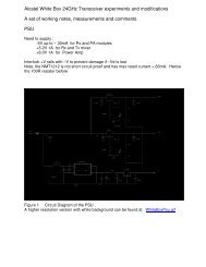
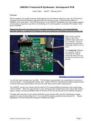
Circuit DescriptionThe complete circuit diagram is shown in Figure 1, with component values shown where they do not have tobe selected for any particular frequency range. The Colpitts VCO based around a UHF bipolar has its outputlightly coupled to a second bipolar buffer followed by a MAR-2 modamp to raise the output to a useful level.A portion of the final RF is tapped off to feed the MC145170 synthesizer device. Dual back-to-back tuningdiodes are used in the VCO to optimise the Q and hence improve phase noise.There is provision on the PCB for either a crystal oscillator – which is part of the MC145170 chip – or anexternal reference by fitting the components appropriate in each case. Connections for either are shown bydotted lines. A trimmer for adjusting the internal reference can be installed using the pad / hole on the PCBthat alternatively serves as the connection for an external referenceThe two Ø V and Ø R outputs from the PLL’s phase detector are taken to an op-amp filter whose componentvalues can be determined either from the spreadsheet at [1] or from any standard PLL design literature. Anextra filter element is available by choice of suitable values for the RC network between the op-amp outputand the tuning diodes. The op-amp type is not shown on the diagram. An NE5532 was used for thebreadboards, but most low noise types will be acceptable. The PCB layout is designed around using one sideof a dual op-amp device with standard connections.An integral 5V regulator supplies the PIC and synthesizer, and this stabilised supply is also used for the VCOand first buffer. Extensive decoupling using chip inductors is applied on each power supply delivery point.The unregulated input voltage is used for biasing the MAR-2 output amplifier and as supply to the op-ampfilter. This allows the VCO tuning voltage to swing over the range typically 2 – 10V .Some component values to start with around the VCO can be found in Appendix 1 .PLL Design information is in Appendix 2PCB LayoutThe double sided PCB is designed to fit into a standard 37 x 55 x 30mm tinplate box such as Type No1000112 available from G3NYK [2]. The component overlay can be seen in Figure 2 All components aresurface mounted, with the majority of R and C being of 0805 size. Decoupling inductors are 0812dimensions but there is enough leeway in pad sizes to allow other device outlines to be squeezed in. All ICsapart from the 78L05 voltage regulator are of the 1.27mm pin spacing SOIC type.The lower side is a continuous groundplane. Pads shown as circular on the layout are connections to ground– use links on home produced PCBs. Spare pads are for connections through, and must be counterbored onthe groundplane side to prevent short circuits.A Mirrored .PDF file of the PCB at 2X scale can be found at [3]Page 3