TK-360G/370G - manuales
TK-360G/370G - manuales
TK-360G/370G - manuales
- No tags were found...

Create successful ePaper yourself
Turn your PDF publications into a flip-book with our unique Google optimized e-Paper software.
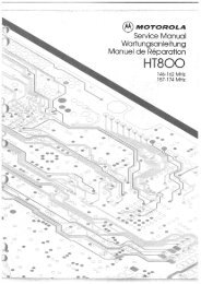
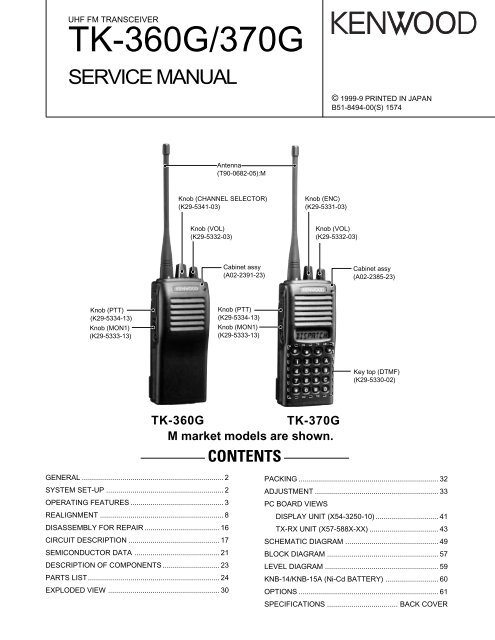
UHF FM TRANSCEIVER<strong>TK</strong>-<strong>360G</strong>/<strong>370G</strong>SERVICE MANUAL© 1999-9 PRINTED IN JAPANB51-8494-00(S) 1574Antenna(T90-0682-05):MKnob (CHANNEL SELECTOR)(K29-5341-03)Knob (ENC)(K29-5331-03)Knob (VOL)(K29-5332-03)Knob (VOL)(K29-5332-03)Cabinet assy(A02-2391-23)Cabinet assy(A02-2385-23)Knob (PTT)(K29-5334-13)Knob (MON1)(K29-5333-13)Knob (PTT)(K29-5334-13)Knob (MON1)(K29-5333-13)Key top (DTMF)(K29-5330-02)<strong>TK</strong>-<strong>360G</strong><strong>TK</strong>-<strong>370G</strong>M market models are shown.CONTENTSGENERAL ...................................................................... 2SYSTEM SET-UP .......................................................... 2OPERATING FEATURES .............................................. 3REALIGNMENT ............................................................. 8DISASSEMBLY FOR REPAIR ..................................... 16CIRCUIT DESCRIPTION ............................................. 17SEMICONDUCTOR DATA .......................................... 21DESCRIPTION OF COMPONENTS ............................ 23PARTS LIST................................................................. 24EXPLODED VIEW ....................................................... 30PACKING ..................................................................... 32ADJUSTMENT ............................................................. 33PC BOARD VIEWSDISPLAY UNIT (X54-3250-10) ............................... 41TX-RX UNIT (X57-588X-XX) .................................. 43SCHEMATIC DIAGRAM .............................................. 49BLOCK DIAGRAM ....................................................... 57LEVEL DIAGRAM ........................................................ 59KNB-14/KNB-15A (Ni-Cd BATTERY) .......................... 60OPTIONS ..................................................................... 61SPECIFICATIONS ................................... BACK COVER
OPERATING FEATURES<strong>TK</strong>-<strong>360G</strong>/<strong>370G</strong>1. Operation Features• <strong>TK</strong>-<strong>360G</strong>Channel selectorRotate to select achannel (1 ~ 8).AntennaLED indicatorLights red whiletransmitting. Lightsgreen while receiving.Flashes orange whilereceiving a 2-Tone orDTMF signal thatmatches the one setup in your transceiver.Flashes red when thebattery power is lowwhile transmitting.PTT (Push-to-Talk) switchPress thisswitch, thenspeak into themicrophone tocall a station.Side 1 keyPress toactivate itsprogrammablefunction.Side 2 keyPress toactivate itsprogrammablefunction.Programmable Auxiliary FunctionsPower switch/Volume controlTurn clockwise toswitch ON thetransceiver.Rotate to adjustthe volume. Toswitch OFF thetransceiver, turncounterclockwisefully.MicrophoneSpeakerSP/MIC jacksConnect anoptional speaker/microphone here.The transceiver isshown with theoptional KNB-14battery pack.Side 1 key and Side 2 key can each be programmedwith one of the following auxiliary functions:• Monitor A (Monitor Unmute–Momentary): Press andhold the Monitor key to hear background noise. Releasethe key to return to normal operation.• Monitor B (Monitor Unmute–Toggle): Momentarilypress the Monitor key to hear background noise. Pressthe key again to return to normal operation.• Monitor C (Carrier Squelch–Momentary): Press andhold the Monitor key to deactivate QT, DQT, 2-Tone, orDTMF signalling. Release the key to return to normaloperation.• Monitor D (Carrier Squelch–Toggle): Momentarilypress the Monitor key to deactivate QT, DQT, 2-Tone, orDTMF signalling. Press the key again to return to normaloperation.• None: No function.• RF Power Lo: Press the RF Power Lo key to toggle theoutput power of a channel between high and low. Thiscan only be used for channels that have beenprogrammed with high power. Pressing RF Power Lowhile using a channel programmed with low powercauses an error tone to sound. (When changing achannel from high to low power, all channelsprogrammed with high power are changed to low.)• 2-Tone Encode Select: To transmit using a 2-Tonecode, press the PTT switch and the 2-Tone EncodeSelect key, then speak into the microphone in yournormal voice.Release the PTT switch and 2-Tone Encode Select keyto receive.• <strong>TK</strong>-<strong>370G</strong>AntennaSpeakerrtyui147qwe2580The transceiver is shown with the optional KNB-14 battery pack.q Rotary encoderYour dealer can program the encoder as eitherGroup Up/Down or Channel Up/Down (defaultsetting). Rotate to select a group or channel. Alsorotate to adjust the squelch in Squelch Adjustmentmode.w LED indicatorLights red while transmitting. Lights green whilereceiving. Flashes orange while receiving a CodeSquelch code or a Selective Call code, or a 2-Toneor DTMF signal that matches the one set up inyour transceiver. Flashes red when the batterypower is low while transmitting.e Power switch/ Volume controlTurn clockwise to switch ON the transceiver.Rotate to adjust the volume. To switch OFF thetransceiver, turn counterclockwise fully.369r PTT (Push-to-Talk) switchPress this switch, then speak into the microphoneto call a station.t Side 1 keyThis is a PF (Programmable Function) key. Pressit to activate its auxiliary function (page 4).y Side 2 keyThis is a PF (Programmable Function) key. Pressit to activate its auxiliary function (page 4).ABCDMicrophoneo!03
OPERATING FEATURES<strong>TK</strong>-<strong>360G</strong>/<strong>370G</strong>9) Reverse (REV) (Note: C type only)When the REV switch is pressed, transmission can beperformed with the receive frequency and receive signaling,and reception can be performed with the trasmit frequencyand transmit signaling.When REV is on, HORN ALERT and PUBLIC ADDRESSdo not work.10) Selectable QT (SEL QT) (<strong>TK</strong>-<strong>370G</strong> M types only)When the SEL QT switch is pressed, QT frequency can betemporarily changed with the CH switch.11) 2-Tone Encode Select (<strong>TK</strong>-<strong>370G</strong> only)1 Press the key programmed as 2-tone Encode Select.• A pre-programmed 2-tone code name appears on thedisplay.2 Press the key programmed as Channel Up and ChannelDown to select you desired 2-tone code name.3 Press PTT switch and 2-Tone Encode Select key to transmitand release them to receive.Note:The code for the <strong>TK</strong>-<strong>360G</strong> is not selectable.You cannot change the tone in step 2 by using the ChannelUp and Channel Down keys.12) Redial (<strong>TK</strong>-<strong>370G</strong> only)Pressing this key when Group/Channel is shown, displaysthe previously transmitted DTMF code. Pressing [PTT] atthis time, transmits the code that is currently displayed.13) RF power lowUsed to temporarily switch transmission output to low power.Turning the function on enables:Hi→Low, Low→LowKey states are backed up, except in the PC mode whenthey are reset.14) Scan (<strong>TK</strong>-<strong>370G</strong> only)Pressing this key starts scanning. Pressing this key againstops scanning.15) Scan Del/Add (<strong>TK</strong>-<strong>370G</strong> only)This key switches the currently displayed channel between"Delete" and "Add".The "Add" channel is contained in the scan sequence, the"Delete" channel is not contained. In the scan mode, this keyswitches the channel between delete or add, temporarily.16) Talk Around (<strong>TK</strong>-<strong>370G</strong> only)Press this key, the transceiver uses the receive frequencyand tone for transmission.The operator can call the other party directly (without repeater).Press this key again, the talk around function goes off.3. Display (<strong>TK</strong>-<strong>370G</strong> only)IconDescriptionNot used in this transceiver.Appears when the selected channel isbusy.Appears when QT, DQT, DTFM, or 2-Tone decoding is deactivated (bypressing the Monitor key).Appears when you receive a CodeSquelch, Selective Call, 2-Tone, orDTMF Signallling call. Also appearswhen you transmit using Code Squelchor Selective Call.Appears while scanning.Appears when using low power on theselected channel.Appears when the selected channel isincluded in the scanning sequence.Displays the selected channel, thesquelch level, DTMF digits (whenentering digits, confirming digits, ormaking a call), and messages receivedvia Selective Call.4. Scan Operating (<strong>TK</strong>-<strong>370G</strong> only)1) Scan types● Single Group ScanYou can scan all valid (ADD) channels in the displayed groupthat can be selected with the group selector.● Multiple Group ScanYou can scan all valid (ADD) channels in all valid (ADD)groups.2) Scan Start ConditionOne or more non-priority channels must be added to allchannels that can be scanned. The transceiver must be innormal receive mode (PTT off).When you activate the key programmed to the scan function,scan starts. The scan icon ("SCN") lights and "SCAN" isindicated on display.17) NoneAn error operation beep sounds, and no action will occur.Use this function when the transceiver is required to beoperated more simply.5
<strong>TK</strong>-<strong>360G</strong>/<strong>370G</strong>OPERATING FEATURES63) Scan Stop ConditionThe scan stops temporarily if the following conditions aresatisfied.1 The receiving signal matches the signalling code in yourradio that is set by the programming software (KPG-56D).2 When the monitor key is depressed.4) Scan Channel Types1 Priority channel is the most important channel for scan,and always detects a signal during scan and when the scanstops temporarily.2 Non-priority channels detect a signal during scan. For thechannels that can be selected with the group or channelselector when the scan does not occur, the "A" icon lights.5) Priority Channel SettingA priority channel can be set as follows with the programmingsoftware (KPG-56D).1 Specify a priority channel as a fixed priority channel.2 Make a selected channel a priority channel.Specify the initial channel before the operator changes it.6) Scan Type According to the Priority Channel1 When no priority channel is set : Only the non-prioritychannels are scanned.If a non-priority channel stops temporarily, it stops untilthere is no signal on the channel.2 When priority channel is set : Either priority channel isscanned.If a non-priority channel stops temporarily, a priority channelsignal is detected at certain intervals.If a priority channel stops temporarily, it stops until there isno signal on the priority channel.7) Revert ChannelThe revert channel is used to transmit during scanning andset by the programming software (KPG-56D).1 PriorityThe transceiver reverts to the priority channel.2 Priority with talkbackThe transceiver reverts to the priority channel.If you press PTT during a resume timer (dropout delay time,TX dwell time) or calling, you can transmit on the currentchannel to answer to the call however revert channel is setto priority channel.After resume time, scan re-starts and the transmissionchannel returns to the priority channel.3 Selected channelThe transceiver reverts to the channel before scanning orthe channel that you changed during scan.4 Last called channelThe transceiver reverts to the last called channel duringscan.5 Last used channelThe transceiver reverts to the last used (transmitted)channel during scan. "Last used" revert channel includestalkback function.6 Selected with talkbackThe transceiver reverts to the channel before scanning orthe channel that you changed during scan.8) Scan EndWhen you reactivate the key programmed to the scanfunction during scan mode, scan ends.The scan icon ("SCN") and "SCAN" or revert channel(programmable) display goes off.9) Temporarily Delete/AddIt is possible to delete or add a channel temporarily duringscan. When scan stops on an unnecessary channel, forexample by interference of the other party, press the delete/add key, then that channel is deleted temporarily and scan willre-start immediately.When you would like to add a deleted channel temporarilyto the scan sequence, select the desired (deleted) channelduring scan, and press the delete/add key before scan re-starts.That channel is added temporarily to the scan sequence.The temporarily deleted or added channels are returned totheir pre-set delete/add conditions when the transceiver exitsfrom scan mode.5. Details of Features1) Time-out timerThe time-out timer can be programmed in 15 secondsincrements from 15 seconds to 300. If the transmitter is keyedcontinuously for longer than the programmed time, thetransmitter is disabled and a warning tone sounds while thePTT button is held down. The alert tone stops when the PTTbutton is released.2) Selective Call Alert LEDYou can select whether or not the LED on the transceiverflashes orange when selective call has occurred.3) PTT IDPTT ID provides a DTMF ANI to be sent with the PTT buttonevery time it is used (Begin of TX ID at beginning oftransmission, End of TX ID at end of transmission, or both).You can program the PTT ID as one of the followings.Off, BOT (Begin of TX ID), EOT (End of PTT ID), BOTH.The contents of ID are programmed for each channel.The transceiver is capable of having ID. The format isDTMF.The timing that the transceiver sends the ID isprogrammable.Begin of TX ID (BOT) : Begin of TX ID is sent at thebeginning of transmission.End of TX ID (EOT) : End of TX ID is sent at the end oftransmission.Both : Begin of TX ID is sent at the beginning of transmissionand End of TX ID is sent at the end of transmission.There is also a "PTT ID" setting for each channel.
OPERATING FEATURES<strong>TK</strong>-<strong>360G</strong>/<strong>370G</strong>4) Battery WarningThis transceiver has a battery warning feature. If low voltageis detected during transmission, the transceiver warns you bya flashing red "LED".When the voltage is detected to be even lower duringtransmission, the transceiver stops transmission and warnsyou by a flashing red "LED" and a beep.Please notice "indication" for the battery exchange, chargingtime by flashing red LED and beep.5) "TOT" Pre-AlertThe transceiver has a "TOT" pre-alert timer. This parameterselects the time at which the transceiver generates a "TOT"pre-alert tone before the "TOT" is expired."TOT" will expire when the selected time passes from theTOT pre-alert tone.6) "TOT" Re-Key TimeThe transceiver has a "TOT" re-key timer. This timer is thetime you cannot transmit after the "TOT" is exceeded. Afterthe "TOT" re-key time expires you can transmit again.7) "TOT" Reset TimeThe transceiver has a "TOT" reset timer. This timer is theminimum wait time allowed during a transmission that will resetthe "TOT" count."TOT" reset time causes the "TOT" to continue even afterthe PTT is released, unless the "TOT" reset timer has expired.8) OST (Operator Selectable Tone) (<strong>TK</strong>-<strong>370G</strong> K typesonly)The transceiver is capable of having the "OST" function and16 tone pairs (QT/DQT) with a max 10-digit name for eachtone pair.9) Clear to TranspondThe transceiver waits for an acknowledgment signal untilthe channel become free.This feature ensures the acknowledgment signal is receiveby another party.10) Battery SaveThis is the automatic battery saver during standby modeoperation. The receiver circuit is turned on and off to conservethe battery life.6. Option Signalling (DTMF/2 tone)Built-in DTMF decoder is available for option signalling.Built-in 2-Tone decoder is available for option signalling.It is possible to use individual call, group call, DBD (DeadBeat Disable). Note : DBD is only DTMFPreset operation is triggered when there is match with OptionSignaling.When Option Signaling matches on a Group Channel whereit is set to Yes, the Option Signaling display flashes and OptionSignaling is canceled. Settings after this will cause "Transpond"or "Alert" to sound.Setting the Selective Call Alert LED will cause the LED tostart flashing orange.Mute or Unmute is triggered by the ID/QT/DQT/Carrier whenoption signaling matches (when Option Signal is deactivatedby a transmission).AND/OROption Signaling match conditions can be selected withAND/OR logic.Alert/Transpond AF Mute OpenAND Triggers at match with QT/ Triggers at match with QT/DQT/ID+DTMF(2tone);Opt DQT/ID+DTMF(2tone);OptOR Triggers at match with QT Triggers only for match with/DQT/ID+DTMF(2tone) ; Opt QT/DQT/ID;SignalingEven if set as OR, there is no Alert/Transpond just withDTMF.Even if set as OR, AF mute cannot be canceled just by amatch with DTMF.In conventional channels not set with QT/DQT, signaling isa match just by receiving the carrier.Auto ResetWhen Option Signaling matches on a Group channel whereit is set to Yes, Option Signaling is canceled when it matches agroup channel set to Yes.After Option Signaling matches, Option Signaling canautomatically Reset after a specified time.Dead Beat DisableWhen the D.B.D (Dead Beat Disable) code matches, apreset operation is performed.When D.B.D matches on all group channels regardless ofwhether Option Signaling = Yes/No, then TX Inhibit or TX RXInhibit is activated by the settings performed afterwards. D.B.Dis canceled when the D.B.D. code + "#" is received.Transpond is always activated when the D.B.D code is amatches. Alert is not output. An Option Signaling match is notdisplayed.7
<strong>TK</strong>-<strong>360G</strong>/<strong>370G</strong>OPERATING FEATURES / REALIGNMENT7. Audible user feedback tones (<strong>TK</strong>-<strong>370G</strong>only)The transceiver outputs various combinations of tones tonotify the user of the transceiver operating state. The maintones are listed belowThe high tone is 1477Hz, the mid tone is 941Hz, and thelow tone is 770Hz.• Power on toneThis tone is output when the transceiver is turned on. (Thehigh tone is output for 500ms.)REALIGNMENT1. ModesUser modePanel test mode(<strong>TK</strong>-<strong>370G</strong> only)PC modeFirmwareprogramming modeClone modePanel tuning modeData programmingmodePC test modeChecksumPC tuning mode• Alert toneThis tone is output when the transceiver is in TX inhibitionfor TOT, battery warning and PLL unlocked. It is output untilthe PTT button is released. (The 697Hz tone is output.)• Busy ToneThis informs the user of a busy channel lock out• Group Call ToneThe group call tone informs the user of a group call in DTMF/2 Tone Option Signaling. This tone repeats 7 times.770Hz770Hz30ms 30ms 30ms• Individual ToneIndividual tone is issued on receiving selective call by DTMF/2 Tone Option Signaling.2000Hz 2000Hz 2000Hz100ms 100ms 100ms 100ms 100ms• Pre Alert toneInforms the user when nearing transmit inhibit (transmitcutoff) time due to TOT.The Pre Alert Tone is issued from the time set for TOT PreAlert until the TOT triggers.1633Hz 1633Hz 1633Hz50ms 50ms 50ms 50ms 50msSelf programmingmode (<strong>TK</strong>-<strong>370G</strong> only)ModeUser modePanel test modePanel tuning modePC modeData programmingmodePC test modeFirmware programmingmodeClone modeSelf programmingmode2. How to Enter Each ModeFunctionFor normal use.Used by the dealer to check thefundamental characteristics.Used by the dealer to tune the radio.Used for communication between theradio and PC (IBM compatible).Used to read and write frequency dataand other features to and from the radio.Used to check the radio using the PC.This feature is included in the FPU.See panel tuning.Used when changing the mainprogram of the flash memory.Used to transfer programming datafrom one radio to another.Frequency, signalling and features.ModeOperationUser modePower ONPanel test mode[2]+Power ON (Two seconds)(<strong>TK</strong>-<strong>370G</strong> only)PC modeReceived commands from PCPanel tuning mode [Panel test mode]+[° ]Firmware programming mode [LAMP]+[MONI]+Power ON(Two seconds)Clone mode[LAMP]+[3]+Power ON(Two seconds)Self programming mode [LAMP]+[ •]+Power ON(Two seconds) (<strong>TK</strong>-<strong>370G</strong> only)3. For the panel Test Mode (<strong>TK</strong>-<strong>370G</strong> only)For the setting method, refer to ADJUSTMENT.3-1. For the panel Tuning ModeFor the setting method, refer to ADJUSTMENT.8
REALIGNMENT<strong>TK</strong>-<strong>360G</strong>/<strong>370G</strong>4. ChecksumExecuting this function, "TUNING" appears on the displayof <strong>TK</strong>-<strong>370G</strong> while calculating the checksum .When the calculation is completed, the display returns tonormal and PC displays the checksum of the radio.5. PC Mode5-1. PrefaceThe <strong>TK</strong>-<strong>360G</strong>/<strong>370G</strong> transceiver is programmed using apersonal computer, a programming interface (KPG-22) andprogramming software (KPG-56D).The programming software can be used with an IBM PC orcompatible. Figure 1 shows the setup of an IBM PC forprogramming.5-2. Connection procedure1. Connect the <strong>TK</strong>-<strong>360G</strong>/<strong>370G</strong> to the personal computer withthe interface cable.2. When the POWER is switched on, user mode can beentered immediately. When the PC sends a command, theradio enters PC mode.When data is transmitted from transceiver, the red LEDblink.When data is received by the transceiver, the green LEDblinks.Notes:• The data stored in the personal computer must match modeltype when it is written into the flash memory.• Change the <strong>TK</strong>-<strong>360G</strong>/<strong>370G</strong> to PC mode, then attach theinterface cable.5-3. KPG-22 description(PC programming interface cable: Option)The KPG-22 is required to interface the <strong>TK</strong>-<strong>360G</strong>/<strong>370G</strong> tothe computer. It has a circuit in its D-subconnector (25-pin)case that converts the RS-232C logic level to the TTL level.The KPG-22 connects the SP/MIC connector of the <strong>TK</strong>-<strong>360G</strong>/<strong>370G</strong> to the computers RS-232C serial port.5-4. Programming software descriptionThe KPG-56D programming disk is supplied in 3-1/2” diskformat. The software on this disk allows a user to program the<strong>TK</strong>-<strong>360G</strong>/<strong>370G</strong> radios via a programming interface cable (KPG-22).5-5. Programming with IBM PCIf data is transferred to the transceiver from an IBM PC withthe KPG-56D, the destination data (basic radio information)for each set can be modified. Normally, it is not necessary tomodify the destination data because their values aredetermined automatically when the frequency range (frequencytype) is set.The values should be modified only if necessary. Data canbe programmed into the flash memory in RS-232C format viathe universal connector.KPG-56D installation manual part No. : B62-1153-XXFig. 16. Firmware Programming Mode6-1. PrefaceFlash memory is mounted on the <strong>TK</strong>-<strong>360G</strong>/<strong>370G</strong>. Thisallows the <strong>TK</strong>-<strong>360G</strong>/<strong>370G</strong> to be upgraded when new featuresare released in the future. (For details on how to obtain thefirmware, contact Customer Service.)6-2. Connection procedureConnect the <strong>TK</strong>-<strong>360G</strong>/<strong>370G</strong> to the personal computer (IBMPC or compatible) with the interface cable (KPG-22).(Connection is the same as in the PC Mode.)6-3. Programming1. Start up the programming software (KPG-56D), select"firmware program" in the "Program" item, and press theReturn key on your personal computer. This starts up thefirmware programmer.2. The top screen is displayed. Press any key to advance tothe next screen.3. Set the communications speed (normally, 57600 bps) andcommunications port in the Setup item.4. Set the firmware to be updated by File select (=F1).5. Hold down the [LAMP] and [MON] switches on the <strong>TK</strong>-<strong>360G</strong>/<strong>370G</strong>, and press the power switch.When the [LAMP] and [MON] switches are held down fortwo seconds, "PROG 576" appears on the display andthe LED lights orange. When "PROG 576" is displayed,release the switches. (<strong>TK</strong>-<strong>370G</strong> only)6. Check the connection between the <strong>TK</strong>-<strong>360G</strong>/<strong>370G</strong> and thepersonal computer, and make sure that the <strong>TK</strong>-<strong>360G</strong>/<strong>370G</strong>is in Program mode.7. Press F10 on the personal computer. A window opens onthe display to indicate the writing progress. When the <strong>TK</strong>-<strong>360G</strong>/<strong>370G</strong> begins to receive data, the LED lights green.8. When data is received successfully, a checksum appearson the display.(Since the <strong>TK</strong>-<strong>360G</strong> does not have a display, check thechecksum with the FPU (KPG-56D).)9
<strong>TK</strong>-<strong>360G</strong>/<strong>370G</strong>REALIGNMENT9. If you want to continue programming other <strong>TK</strong>-<strong>360G</strong>/<strong>370G</strong>s, repeat steps 5 to 8.Notes:● To start the Firmware Programmer from KPG-56D, the Fpropath must be set up by the KPG-56D Setup.● This mode cannot be entered if the Firmware Programmingmode is set to Disable in the Programming software (KPG-56D).● When programming the firmware, it is recommend to copythe data from the floppy disk to your hard disk before youupdate the radio firmware.Directly copying from the floppy disk to the radio may notwork because the access speed is too slow.6-4. Function1. If you press the [MON] switch while "PROG XXX" isdisplayed, the checksum is displayed. If you press the[MON] switch again (while the checksum is displayed),"PROG XXX" is redisplayed.2. A transmission speed can be selected by pressing the[LAMP] switch while "PROG XXX" is displayed.12900 bps: The LED flashes green and red alternately.38400 bps: The LED flashes orange.57600 bps: The LED lights orange.PTT/RXDNote: You can clone the programmed data between thetransceiver listed below.Frequency version must be same.Slave <strong>TK</strong>-<strong>360G</strong> <strong>TK</strong>-<strong>360G</strong> <strong>TK</strong>-860G <strong>TK</strong>-860GK M K MMaster<strong>TK</strong>-<strong>370G</strong> <strong>TK</strong>-<strong>370G</strong> <strong>TK</strong>-862G <strong>TK</strong>-862GK M K M<strong>TK</strong>-<strong>370G</strong>K<strong>TK</strong>-<strong>370G</strong>M3.5Cloning cable parts No.E30-3410-05 (<strong>TK</strong>-<strong>370G</strong>➝<strong>TK</strong>-<strong>360G</strong>/<strong>370G</strong>)2.5GNDREMOTE/TXDE30-3411-05 (<strong>TK</strong>-<strong>370G</strong>➝<strong>TK</strong>-860G/862G)2.53.5Note:Normally, write in the high-speed mode.7. Clone ModeProgramming data can be transferred from one radio toanother by connecting them via their SP/MIC connectors. Theoperation is as follows (the transmit radio is the master andthe receive radio is the slave).PTT/RXDGNDREMOTE/TXD8118MBLPSBGNDPTT/RXDMEMICREMOTE/TXDCM1. Turn the master <strong>TK</strong>-<strong>370G</strong> power ON with the [LAMP]+[3]key held down. The <strong>TK</strong>-<strong>370G</strong> displays " CLONE ".2. Power on the slave <strong>TK</strong>-<strong>360G</strong>/<strong>370G</strong>.3. Connect the cloning cable to the SP/MIC connectors onthe master and slave.4. Press the ] key on the master while the master displays" CLONE[° ". The data of the master is sent to the slave.While the slave is receiving the data, "-PC-" is displayed.When cloning of data is completed, the master displays"END", and the slave automatically operates in the Usermode. The slave can then be operated by the same programas the master.5. The other slave can be continuously cloned. When the [° ]key on the master is pressed while the master displays"END", the master displays " CLONE ". Carry out theoperation in steps 2 to 4.Cloning cableFig. 210
REALIGNMENT<strong>TK</strong>-<strong>360G</strong>/<strong>370G</strong>8. Self Programming Mode (<strong>TK</strong>-<strong>370G</strong>)Write mode for frequency data and signalling etc. Mainlyused by the person maintaining the user equipment.8.1 Self programming mode settingRemove D17 from the TX-RX unit (Figure 3) (K modelsonly). Hold down the [LAMP]+[●] switches and turn thepower switch on.When the self programming mode is entered, [SELF]appears on the display. The mode changes automaticallyto Model Select Mode and “PORTABLE” is displayed inabout one second.Note :This mode (self programming mode) cannot be set when ithas been disabled with the FPU.X57-588XCompoent SideFig. 3D17●Flow ChartRadio type Portable[CH]Mobile[2][CH]Radio Band & Channel Type VHF 8CH[CH]VHF 128CH[CH]UHF 8CH[CH]UHF 128CH[2][CH]Frequency VersionVHF F1 VHF F2 UHF F1 UHF F3 UHF F4[CH][CH][CH][CH]Cannot be Cannot be[3][2]set when set whenPortable is Mobile isSelf programming modeselectselect[MON]Channel set mode[LAMP]Function set modeNote :IF the radio type of <strong>TK</strong>-<strong>370G</strong> was temporally set to "Mobile"for the cloning purposes, "UNPROG" is displayed (at UserMode) when the <strong>TK</strong>-<strong>370G</strong> is turned on.In this case, please set the radio type back to "Portable" atModel Select Mode menu.8-2. Channel Setting ModeThis is a mode for making channel settings with the panelkeys without using the FPU.Pressing [MON] when "SELF" is displayed, sets ChannelSetting Mode.Select an item set using [3] then change the selection withthe encoder.The data displayed using [2] is stored in the memory andthen proceeds to the next item. Pressing [3] proceeds tothe next item without storing it in the memory.Press [MON] to set the display to "SELF" and return to reset(default) status.No. Function Choices Display RemarksSelect 1-128 _1-_1._ [3] : Group selection/Channel _1-128._ Channel selection changeSelect 1-128 _1.-_1_Group128.-_1_1 RX frequency Step 2.5kHz-1MHz STP_250 Display when an item is selectedSTP_1000 or when a step is changed(about 0.5 seconds)[ •] Step changeUHF : 5.0,6.25kHz,1MHz,StepBlank ———— [LAMP] : Freq On/Blank switching100.0000- R.100.0000 The rightmost dot indicates550.0000MHz50Hz digit (On=5; Off=0).2 Rx Signaling OFF ———— [LAMP] : Off/QT/DQT switchingQT 67.0-250.3Hz QT_67.0_ [ •] : Mode switching(EIA Mode) QT_250.3_ [° ] : Normal/InverseQT 67.0-250.3Hz QT_67.0* switching(0.1Hz Step Mode) QT_250.3*DQT 000-777 (Normal) DQT000N*(1 Step Mode) DQT777N*DQT 023-754 (Normal) DQT023N(Standard Table Mode) DQT754NDQT 000-777 (Inverse) DQT000I*(1 Step Mode) DQT777I*DQT 023-754 (Inverse) DQT023I(Standard Table Mode) DQT754I11
<strong>TK</strong>-<strong>360G</strong>/<strong>370G</strong>REALIGNMENTNo. Function Choices Display Remarks3 TX frequency Step 2.5kHz-1MHz STP_250 Same as RX frequency.STP_1000Blank ————100.0000- T.100.0000550.0000MHz4 TX Signaling Same as RX signaling.5 Option Signaling OFF NONE____ DefaultDTMFDTMF____2-TONE2TONE___6 ID 000- ___ID___ Display when an item is selected9999999999 (about 0.5 seconds)12345678 Display of the current setting(If it is 8 or more digits, scroll it.)——987 Display when a code is input(Input it with DTMF key.)Blank ———— [LAMP] : Data clear7 Busy Channel NO BCL_NO__ DefaultLockout Type 1 BCL_1___ BCL_YES for K typeType 2 BCL_2___ N/A for K type8 Beat shift No SHFT_NO_ DefaultYesSHFT_YES9 RF Power High Power PWR_H___ DefaultLow Power PWR_L___10 Wide/Narrow Wide WIDE____Narrow NARROW__11 Scan DELETE SCAN_DEL Not used for <strong>TK</strong>-<strong>360G</strong>Delete/ADD ADD SCAN_ADD Default12 Priority No P.CH_NO__ Not used when (Scan) Priority is not Fixed.Channel Yes P.CH_YES_13 Home Channel No H.CH_NO__ Not used when Home Channel isYes H.CH_YES_ not set in Key Assignment.14 Compander No COMP_NO_ Not used when Wide is selected.YesCOMP_YES15 PTT ID OFF P.ID_OFFBegin of TX P.ID_1End of TX P.ID_2BothP.ID_316 Begin of 000- _BOT_ID_ Not valid if Dial ID =Disable andTX ID 9999999999999999 PTT ID=OFF, or EOT is set.Display when an item is selected(about 0.5 seconds)12345678 Display of the current setting(If it is 8 or more digits, scroll it.)——987 Display when a code is input(Input it with DTMF key.)Blank ———— [LAMP] : Data clear17 END of 000- _EOT_ID_ Not valid if Dial ID=Disble andTX ID 9999999999999999 PTT ID=OFF, or BOT is set.Display when an item is selected(about 0.5 seconds)12345678 Display of the current setting(If it is 8 or more digits, scroll it.)——987 Display when a code is input(Input it with DTMF key.)Blank ———— [LAMP] : Data clear● Flow ChartChannel Setting ModeSelf programming mode[MON][MON]Channel set mode[2][MON]RX frequency[2]/[3][MON]RX signaling[2]/[3][MON]TX freguency[2]/[3][MON]TX signaling[2]/[3][MON]option signaling[2]/[3][MON]ID[2]/[3][MON]Busy channel lockout[2]/[3][MON]Best Shift yes/no[2]/[3][MON]RF Power High/Low[2]/[3][MON]Wide/Narrow[2]/[3][MON]Scan delete/add[2]/[3][MON]Priority channel[2]/[3][MON]Home channel[2]/[3][MON]Compander yes/no[2]/[3][MON]PTT ID[2]/[3][MON]Begin of TX ID[2]/[3][MON]End of TX ID[2]/[3][LAMP][LAMP][LAMP][LAMP][LAMP][LAMP][LAMP]OFFOFFOFFChannel selection[LAMP][LAMP]Group selectionQT DQT N DQT I[LAMP] [ ][LAMP]OFF QT DQT N DQT I[LAMP][LAMP] [ ]Data clearNot used when Wide is selected.Data clearData clear[3]Not used when (Scan) Priority is not Fixed.Not used when Home Channel is not set in key Assignment.Not valid if Dial ID=Disableand PTT ID=off, or EOT is set.Not valid if Dial ID=Disableand PTT ID=off, or BOT is set.12
REALIGNMENT<strong>TK</strong>-<strong>360G</strong>/<strong>370G</strong>8-3. Function Setting ModeThis is a mode for using the panel keys to make functionsettings without using the FPU, that operate on all channels.Pressing the [LAMP] when "SELF" is displayed, sets theFunction Setting Mode.Select an item set using [3] then change the selection withthe encoder.The data displayed using [2] is stored in the memory andthen proceeds to the next item. Pressing [3] proceeds tothe next item without storing it in memory.Press [LAMP] to display "SELF" and return to reset (default)status.Function Setting ModeNo. Function Choices Display RemarksFunction Key1 [LAMP] No Function LAMP_OFFTalk Around LAMP_3 * <strong>TK</strong>-<strong>360G</strong> cannot be selected.K and M destinations onlyDisplay Character LAMP_5 * <strong>TK</strong>-<strong>360G</strong> cannot be selected.Home Channel LAMP_7 * <strong>TK</strong>-<strong>360G</strong> cannot be selected.Channel Down LAMP_8 * <strong>TK</strong>-<strong>360G</strong> cannot be selected.Channel Up LAMP_9 * <strong>TK</strong>-<strong>360G</strong> cannot be selected.Keylock LAMP_10 * <strong>TK</strong>-<strong>360G</strong> cannot be selected.Lamp LAMP_11 Default(<strong>TK</strong>-<strong>370G</strong>)Selectable QT LAMP_15Monitor AMonitor BMonitor CMonitor DRF Power LowLAMP_17LAMP_18LAMP_19LAMP_20LAMP_21* <strong>TK</strong>-<strong>360G</strong> cannot be selected.* <strong>TK</strong>-<strong>360G</strong> cannot be selected.M destination onlyScan LAMP_22 * <strong>TK</strong>-<strong>360G</strong> cannot be selected.Scan DEL/ADD LAMP_23Group Down LAMP_24* <strong>TK</strong>-<strong>360G</strong> cannot be selected.* <strong>TK</strong>-<strong>360G</strong> cannot be selected.Group Up LAMP_25 * <strong>TK</strong>-<strong>360G</strong> cannot be selected.Scramble LAMP_26 Only when scrambler is set2 [MONI] No Function MON_OFFTalk Around MON_3Display Character MON_5* <strong>TK</strong>-<strong>360G</strong> cannot be selected.* <strong>TK</strong>-<strong>360G</strong> cannot be selected.Home Channel MON_7 * <strong>TK</strong>-<strong>360G</strong> cannot be selected.Channel Down MON_8 * <strong>TK</strong>-<strong>360G</strong> cannot be selected.Channel Up MON_9* <strong>TK</strong>-<strong>360G</strong> cannot be selected.Keylock MON_10 * <strong>TK</strong>-<strong>360G</strong> cannot be selected.Lamp MON_11 * <strong>TK</strong>-<strong>360G</strong> cannot be selected.Selectable QT MON_15 * <strong>TK</strong>-<strong>360G</strong> cannot be selected.M destination onlyMonitor A MON_17 DefaultNo. Function Choices Display Remarks2 [MONI] Monitor B MON_18Monitor CMonitor DMON_19MON_20RF Power Low MON_21Scan MON_22 * <strong>TK</strong>-<strong>360G</strong> cannot be selected.Scan DEL/ADD MON_23 * <strong>TK</strong>-<strong>360G</strong> cannot be selected.Group Down MON_24* <strong>TK</strong>-<strong>360G</strong> cannot be selected.Group Up MON_25 * <strong>TK</strong>-<strong>360G</strong> cannot be selected.Scrambler MON_26 Only when scrambler is set3 ]<strong>TK</strong>-<strong>370G</strong> No Function KEY1_OFF[° only Talk Around KEY1_3 K and M destinations onlyDisplay Character KEY1_5Home ChannelChannel DownKEY1_7KEY1_8Channel Up KEY1_9KeylockLampKEY1_10KEY1_11Selectable QT KEY1_15Monitor AMonitor BMonitor CMonitor DKEY1_17KEY1_18KEY1_19KEY1_20RF Power Low KEY1_21ScanKEY1_22M destination onlyScan DEL/ADD KEY1_23 DefaultGroup Down KEY1_24Group UpKEY1_25Scrambler KEY1_26 Only when scrambler is set4 [ •]<strong>TK</strong>-<strong>370G</strong> No Function KEY2_OFFonly Talk Around KEY2_3 K and M destinations onlyDisplay Character KEY2_5Home Channel KEY2_7Channel Down KEY2_8Channel Up KEY2_9KeylockLampKEY2_10KEY2_11Selectable QT KEY2_15Monitor AMonitor BMonitor CMonitor DKEY2_17KEY2_18KEY2_19KEY2_20RF Power Low KEY2_21ScanKEY2_22Scan DEL/ADD KEY2_23Group Down KEY2_24M destination onlyGroup Up KEY2_25Scrambler KEY2_26 Only when scrambler is set13
<strong>TK</strong>-<strong>360G</strong>/<strong>370G</strong>REALIGNMENT14No. Function Choices Display Remarks No. Function Choices Display Remarks5 [2]<strong>TK</strong>-<strong>370G</strong> No Function KEY3_OFFonly Talk Around KEY3_3 DefaultDisplay Character KEY3_5Home Channel KEY3_7Channel Down KEY3_8Channel Up KEY3_9Keylock KEY3_10Lamp KEY3_11Selectable QT KEY3_15 M destination onlyMonitor A KEY3_17Monitor B KEY3_18Monitor C KEY3_19Monitor D KEY3_20RF Power Low KEY3_21 DefaultScan KEY3_22Scan DEL/ADD KEY3_23Group Down KEY3_24Group Up KEY3_25Scrambler KEY3_26 Only when scrambler is set6 [3]<strong>TK</strong>-<strong>370G</strong> No Function KEY4_OFFonly Talk Around KEY4_3Display Character KEY4_5Home Channel KEY4_7Channel Down KEY4_8Channel Up KEY4_9Keylock KEY4_10Lamp KEY4_11Selectable QT KEY4_15 M destination onlyTX Code KEY4_16Monitor A KEY4_17Monitor B KEY4_18Monitor C KEY4_19Monitor D KEY4_20RF Power Low KEY4_21 DefaultScan KEY4_22Scan DEL/ADD KEY4_23Group Down KEY4_24Group Up KEY4_25Scrambler KEY4_26 Only when scrambler is set7 [CH] Channel Up/Down CH_UP/DN DefaultGroup Up/Down GR_UP/DNNo Function KNOB_OFFOptional Feature8 Power On Tone YES/NO PONT_YES Default:YES9 Control Tone YES/NO CNTT_YES Default:YES10 Warning Tone YES/NO WART_YES Default:YES11 Time Out Timer OFF,15-300/15s Step TOT_60 Default:60s12 TOT OFF,1-10/ TOTP_PFF Cannot be set when TOT is OFF.Pre-Alert Time 1s StepDefault:OFF13 TOT OFF1-60/ TO<strong>TK</strong>_OFF Cannot be set when TOT is OFF.Rekey Time 1s Step Default:OFF14 TOT OFF1-15/ TOTS_OFF Cannot be set when TOT is OFF.Reset Time 1s StepDefault:OFF15 Clear to Transpond YES CTT_YES(BCL for Transpond) NO CTT_NO Default16 Battery Save ON BATT_ON DefaultOFF BATT_OFF17 Signaling OR SIG__OR DefaultAND SIG_AND18 Squelch Level 0-9/1 Step SQL__5 Default;519 Priority None PRI_NONE DefaultFixed PRI_FIX_Selected PRI_SEL_20 Lock Back 0.5-5.0/0.05 LBA_500 Default:500ms Cannot beTime Aset when Priority = none.21 Lock Back 0.5-5.0/0.05 LBB_2000 Default:2000ms CannotTime Bbe set when Priority = none.22 Revert Selected REV_SELChannel Last Called REV_L/C_ DefaultLast Used REV_L/U_Selected + Talk Back REV_S/T_Priority REV_PRI_Priority + Talk Back REV_P/T_23 Dropout 0-300/1s DODT___3 Default;3sDelay Time24 Dwell Time 0-300/1s DWL___3 Default;3sDTMF25 Digit Time 50-200/10ms DIGT__50 Default;50ms26 Inter Digit Time 50-1000/50ms IDT___50 Default;50ms27 First Digit Time 50-200/10ms FDT___50 Default;50ms28 First Digit Delay 50-1000/50ms RIST_100 Default;100ms29 Rise Time with QT 50-1000/50ms RTWQ_100 Default;100ms30 DIAL ID Enable DID_ENADisable DID_DIS Default31 No.of 12Key NODK_12 DefaultDTMF Key 16Key NODK_1632 DTMF Hold Time ON DHT__ON DefaultOFF DHT__OFF33 Store and Send Enable SAS_ENADisable SAS_DIS Default34 D Key D Code DKA_D_CD DefaultAssignment 1-16/1s DKA_16__35 DTMF Code SQ DTMF_CSQ DefaultSignaling SEL CALL DTMF_SEL36 Inter Mediaate 0-9,A-D,*,# IMC__#_ Default: # (Can be set only whenCodeDTMF signaling = SEL CALL.)
REALIGNMENT<strong>TK</strong>-<strong>360G</strong>/<strong>370G</strong>No. Function Choices Display Remarks●Flow Chart37 Group Code A-D,*,# GPCD_FF_ Default;OFF38 Auto Rest OFF ART_OFF_Time 1-15/1s ART__10 Default;10s39 Call Alert/ OFF CA/T_OFF DefaultTranspond Call Alert CA/T_C/ATranspond CA/T_T/A(Call Alert)Transpond CA/T_T/I(ID Code)Transpond CA/T_T/T(Transpond Code)Others40 Panel Test/panel Enable PTM_ENA Default (Not used for <strong>TK</strong>-<strong>360G</strong>.)Tuning MODE Disable PTM_DISFunction Setting ModeSelf programming mode[LAMP][LAMP]Function set mode[LAMP][LAMP] key function[2]/[3][LAMP][MON] key function[2]/[3][LAMP][ ] key function[2]/[3][LAMP][ ] key function[2]/[3][LAMP][2] key function[LAMP][LAMP][LAMP][LAMP][LAMP][LAMP][LAMP]Squelch level[2]/[3]Priority[2]/[3]Look back time A[2]/[3]Look back time B[2]/[3]Revert channel[2]/[3]Dropout delay time[2]/[3]Dwell time[LAMP][LAMP][LAMP][LAMP]Group codeAuto reset timeCall alert/TranspondPanel test/Panel tuningmode[2]/[3][2]/[3][2]/[3]8-4. Memory Reset ModeThis mode is used to clear data for functions that can be setin Self Programming Mode or to return to reset values (default).Pressing ] when "SELF" is shown, sets the display to"CANCEL".[°Turning the encoder alternately switches the displaybetween "CANCEL" "READY".Pressing ] when "READY" is shown, clears the data andsets the display to "CLEAR".Pressing ] again, returns the display to "SELF".Pressing[° ] when "CANCEL" is shown, returns the displayto "SELF" without[° resetting the data.When the ] switch is pressed while "SELF" is displayed,the memory[° is reset.When the memory is reset, mode data and model data arenot reset.The <strong>TK</strong>-<strong>360G</strong> cannot reset the memory.[LAMP][LAMP][LAMP][LAMP][LAMP][LAMP][LAMP][LAMP][2]/[3][3] key function[2]/[3][CH] key function[2]/[3]Power on tone yes/no[2]/[3]Contorol tone yes/no[2]/[3]WArning tone yes/no[2]/[3]Time Out Timer[2]/[3]T.O.T. Pre-alert time[2]/[3]T.O.T. Rekey time[LAMP][LAMP][LAMP][LAMP][LAMP][LAMP][LAMP][LAMP][2]/[3]Digit time[2]/[3]Inter digit time[2]/[3]First digit time[2]/[3]First digit delay[2]/[3]Rise time with QT[2]/[3]Dial ID[2]/[3]No. of DTMF key[2]/[3]DTMF hold time[LAMP][2]/[3]T.O.T. Reset time[LAMP][2]/[3]Store & Send[LAMP][2]/[3]Clear to Transpond[LAMP][2]/[3]D key assignment[LAMP][2]/[3]Battery Save on/off[LAMP][2]/[3]DTMF signaling[LAMP]Signaling[2]/[3][LAMP]Inter mediate code[2]/[3][2]/[3][2]/[3]15
<strong>TK</strong>-<strong>360G</strong>/<strong>370G</strong>DISASSEMBLY FOR REPAIRSeparating the case assembly from the chassis.1. Remove the two knobs z and three round units x.2. Remove the two screws c.3. Expand the right and left sides of the bottom of the caseassembly, lift the chassis, and remove it from the caseassembly v.Separating the chassis from the unit.• <strong>TK</strong>-<strong>360G</strong>1. Remove the twelve small screws m, and remove the threelarge screws ,.2. Remove the solder from the antenna terminal using a solderiron then lift the unit off (X57).ccxxzx zx z• <strong>TK</strong>-<strong>370G</strong>1. Remove the three screws ..Lift the unit (X54), and rise up the connecter lever in thearrow with your finger /.Remove the three hexagonal bosses -, 11 and remove thetwelve screws m.2. Remove the solder from the antenna terminal using asoldering iron, then lift the unit off (X57).<strong>TK</strong>-<strong>370G</strong>v..X54-4. Taking cure not to cut the speaker lead b, open the chassis andcase assembly, and pull the speaker lead with connector n..Ω,Ω/ X57-CN1Ωmm m m m, mmmmmmAntenna teminalmX57-,bCN3n16
CIRCUIT DESCRIPTION<strong>TK</strong>-<strong>360G</strong>/<strong>370G</strong>1. Frequency configurationThe receiver utilizes double conversion. The first IF is 49.95MHz and the second IF is 450 kHz. The first local oscillatorsignal is supplied form the PLL circuit.The PLL circuit in the transmitter generates the necessaryfrequencies. Fig. 1 shows the frequencies.ANTANTSWPAAMPTX/RX : 450~470MHzRFAMPTXAMPFig. 12. ReceiverANT5Fig. 2MCF49.95MHzRX : 400.05~420.05MHzTX : 450~470MHzCF450kHzIFSYSTEM50.4MHzX3multiplyPLLVCOFrequency configurationReceiver sectionAFAMPTCXOMICAMP1) Front end (RF AMP)The signal coming form the antenna passes through thetransmit/receive switching diode circuit, (D3,D7) passesthrough a BPF, and is amplified by the RF amplifier (Q301).The resulting signal passes through a BPF and goes to themixer.2) First mixerThe signal from the front end is mixed with the first localoscillator signal generated in the PLL circuit by Q19 toproduce a first IF frequency of 49.95 MHz.The resulting signal passes through the XF1 MCF to cutthe adjacent spurious and provide the optimumcharacteristics, such as adjacent frequency selectivity.SP16.8MHzMICThe frequency configuration of the receiver is shown in Fig. 2.ANTSWBPFRFAMPQ301CF1 : WideCF2 : NarrowIC4IF, MIX, DET2nd LocalX3 multiplyQ12AF AMPIC16 (2/2)TCXOIC14 2 1HPF LPF HPF BEFBPFMIXERQ191st LocalDE-EMPMCFXF1PLLVCOAF AMPIC15(2/2)EXPIF AMPQ22MUTEAF VOL41AF AMPIC11SP3) IF Amplifier circuitThe first IF signal is passed through a four-pole monolithiccrystal filter (XF1) to remove the adjacent channel signal.The filtered first IF signal is amplified by the first IF amplifier(Q22) and then applied to the lF system IC (IC4). The IFsystem IC provides a second mixer, second local oscillator,limiting amplifier, quadrature detector and RSSI (ReceivedSignal Strength Indicator). The second mixer mixes the firstIF signal with the 50.4MHz of the second local oscillatoroutput (TCXO X3) and produces the second IF signal of450kHz.The second IF signal is passed through the ceramic filter(CF1; Wide, CF2 ; Narrow) to remove the adjacent channelsignal. The filtered second IF signal is amplified by thelimiting amplifier and demodulated by the quadraturedetector with the ceramic discriminator (CD1). Thedemodulated signal is routed to the audio circuit.4) Wide/Narrow changeover circuitNarrow and Wide settings can be made for each channelby switching the ceramic filters CF1 (Wide) and CF2(Narrow).The WIDE (high level) and NARROW (low level) data isoutput from IC5 (OUTPUT EXPANDER), pin 4.When a WIDE (high level) data is received, Q14 turn offand Q17 turn on. When a NARROW (low level) data isreceived, Q14 turn on and Q17 turn off. D14 and D13 areswitched to ceramic filters when a high/low level data isreceived.Q23 turns on/off with the Wide/Narrow data and the IC4detector output level is changed to maintain a constantoutput level during wide or narrow signals.C2635RFig. 35RQ14Q17C265C133 CD1AFOR78R108IFOQADMXOIFIC108D14R75R81R105Q22R98MXICF1CF2R80W/NQ23IC4FM IF SYSTEMR74C107D13R79W/N"H" : Wide"L" : NarrowWide/Narrow changeover circuit17
<strong>TK</strong>-<strong>360G</strong>/<strong>370G</strong>CIRCUIT DESCRIPTION5) Audio amplifier circuitThe demodulated signal from IC4 is amplified by IC16 (2/2),high-pass filtered, low-pass filtered, high-pass filtered, bandeliminatefiltered, and de-emphasized by IC14.The signal then goes through an AF amplifier IC15 (2/2), anAF volume control (VR2), and is routed to an audio poweramplifier (IC11) where it is amplified and output to the speaker.6) SquelchPart of the AF signal from the IC enters the FM IC (IC4)again, and the noise component is amplified and rectifiedby a filter and an amplifier to produce a DC voltagecorresponding to the noise level.The DC signal from the FM IC goes to the analog port ofthe microprocessor (IC13). IC13 determines whether tooutput sounds from the speaker by checking whether theinput voltage is higher or lower than the preset value.To output sounds from the speaker, IC6 sends a high signalto the SP MUTE line and turns IC11 on throughQ32,Q33,Q34 and Q30. (See Fig. 4)7) Receive signaling(1) QT/DQT (Low-speed data)300Hz and higher audio frequencies of the output signal fromIF IC are cut by a low-pass filter (IC19). The resulting signalenters the microprocessor (IC13). IC13 determines whetherthe QT or DQT matches the preset value, and controls theSP MUTE and the speaker output sounds according to thesquelch results.(2) 2-TONE (High-speed data)Part of the received AF signal output from the AF amplifierIC16(2/2), and then pass through an audio processor (IC14),goes to the other AF amplifier IC15(1/2), is compared, andthen goes to IC13. IC13 checks whether 2-TONE data isnecessary. If it matches, IC13 carries out a specifiedoperation, such as turning the speaker on. (See Fig. 4)FM IF IC4IF AMP DETIC16 (2/2)IF AMP5IC14 2 1HPF LPF HPF BEFDE-EMP43EXPMUTE41(3) DTMF (High-speed data)The DTMF input signal from the IF IC(IC4) is amplified byIC16(2/2) and goes to IC18, the DTMF decoder. The decodedinformation is then processed by the CPU. Duringtransmission and standby, the DTMF IC is set to the powerdown mode when the PD terminal is High. When the line isbusy, the PD terminal becomes Low, the power down modeis canceled and decoding is carried out.3. PLL frequency synthesizerThe PLL circuit generates the first local oscillator signal forreception and the RF signal for transmission.1) PLLThe frequency step of the PLL circuit is 5 or 6.25kHz.A 16.8MHz reference an oscillator signal is divided at IC2 by afixed counter to produce oscillator (VCO) output signal whichis buffer amplified by Q3 then divided in IC2 by a dual-moduleprogrammable counter. The divided signal is compared inphase with the 5 or 6.25kHz reference signal from the phasecomparator in IC2. The output signal from the phasecomparator is filtered through a low-pass filter and passed tothe VCO to control the oscillator frequency.(See Fig. 5)2) VCOThe operating frequency is generated by Q2 in transmitmode and Q10 in receive mode. The oscillator frequency iscontrolled by applying the VCO control voltage, obtained fromthe phase comparator, to the varactor diodes (D2 and D4 intransmit mode and D9 and D11 in receive mode). The T/R pinis set high in receive mode causing Q7 and Q8 to turn Q2 offand turn Q10 on.The T/R pin is set low in transmit mode. The outputs fromQ10 and Q2 are amplified by Q3 and sent to the bufferamplifiers.D2, 4Q2TX VCOQ1RF AMPIC15 (2/2)AF AMPIC11AF PA AMPQ30SWSPLPFQ3BUFF AMPQ4RF AMPQ32, 33, 34SWD9, 11Q10RX VCOQ7, 8T/R SW93ANSQLIC13CPU95TOIIC19LPFQT/DQT2TN3Fig. 4IC15 (1/2)COMPARATER2-TONEPD, CLK, SD,STDIC18DTMFDECODEQ36SWAF Amplifier and Squelch5IC65RC7SPMUTEOUTPUT EXPANDERPLL DATAREF OSCPLL IC IC2I/N5kHz/6.25kHzPHASECOMPARATORCHARGEPUMPI/M5kHz/6.25kHz1816.8MHzFig. 5 PLL circuit
CIRCUIT DESCRIPTION<strong>TK</strong>-<strong>360G</strong>/<strong>370G</strong>3) UNLOCK DETECTORIf a pulse signal appears at the LD pin of IC2, an unlockcondition occurs, and the DC voltage obtained form D1,R1, and C6 causes the voltage applied to the microprocessorto go low. When the microprocessor detects this condition,the transmitter is disabled, ignoring the push-to-talk switchinput signal.(See Fig. 6)5CFromT/R SW(D5)Q5Pre-DRIVEAMP+BAPC(IC13)R56R57R58Q6DRIVEAMPIC3(1/2)IC1RFPOWER AMPVDDIC3(2/2)VGGD3ANTSWLPFANTIC2LDD1R1IC13ULFig. 8 Drive and final amplifier and APC circuitPLL ICFig. 6 Unlock detector circuit4. Transmitter System1) Microphone amplifierThe signal from the microphone passes through the limittercircuit in D23, and through the high-pass filter, the ALCcircuit, the low-pass filter, the high-pass filter, and preemphasis/IDCcircuit IC14. When encoding DTMF, the muteswitch (Q35) is turned OFF for muting the microphone inputsignal.The signal passes through the D/A converter (IC17) for themaximum deviation adjustment, and goes to the VCXOMICmodulation input.C6MUTEQ35SWFig. 7 Microphone amplifierMPUIC14 15 16 18 19 9 8D2312HPF ALC COMP LPF HPFPRELIMITEMPIDCIC17D/ALPFTOVCO22VCOQT/DQTTOTCXO20IC13CPU 2DTMF/ 2 TONELPFDTMF/2 TONEX1TCXO(RX Audio)LPF6AFAMPIC15(2/2)2) Drive and Final amplifierThe signal from the T/R switch (D5 is on) is amplified by thepre-drive (Q5) and drive amplifier (Q6) to 50mW.The output of the drive amplifier is amplified by the RF poweramplifier (IC1) to 4.0W (1W when the power is low). TheRF power amplifier consists of two MOS FET stages. Theoutput of the RF power amplifier is then passed through theharmonic filter (LPF) and antenna switch (D3 is on) andapplied to the antenna terminal.3) APC circuitThe APC circuit always monitors the current flowing throughthe RF power amplifier (IC1) and keeps a constant current.The voltage drop at R56, R57 and R58 is caused by thecurrent flowing through the RF power amplifier and thisvoltage is applied to the differential amplifier IC3(1/2).IC3(2/2) compares the output voltage of IC3(1/2) with thereference voltage from IC13, and the output of IC3(2/2)controls the VGG of the RF power amplifier to make bothvoltages the same.The change of power high/low is carried out by the changeof the reference voltage.4) Encode signaling(1) QT/DQT (Low-speed data)QT,DQT data of the TOTCXO Line is output form pin 20 ofthe CPU. The signal passes through a low-pass CR filterand goes to the TCXO(X1).The QT,DQT data of the TOVCO Line is output form pin 22of the CPU. The signal passes through a low pass CR filter,mixes with the audio signal, and goes to the VCO modulationinput. TX deviation is adjusted by the CPU. (See fig.7)(2) DTMF/2 TONE (High speed data)High-speed data is output from pin 2 of the CPU. The signalpasses through a low-pass CR filter, and provides a TXand SP out tone, and is then applied to the audio processor(IC14). The signal is mixed with the audio signal and goesto the VCO.TX deviation is adjusted by the CPU. (See fig.7)5. Power supplyThere are five 5V power supplies for the microprocessor:5V,5M,5C,5R, and 5T. 5V for microprocessor is alwaysoutput while the power is on. 5M is always output, but turnsoff when the power is turned off to prevent malfunction ofthe microprocessor.5C is a common 5V and is output when SAVE is not set toOFF.5R is 5V for reception and output during reception.5T is 5V for transmission and output during transmission.19
<strong>TK</strong>-<strong>360G</strong>/<strong>370G</strong>CIRCUIT DESCRIPTION6. Control CircuitThe control circuit consists of a microprocessor (IC13) andits peripheral circuits. It controls the TX-RX unit and transfersdata to and from the display unit. IC13 mainly performs thefollowing:(1) Switching between transmission and reception by thePTT signal input.(2) Reading system, group, frequency, and program datafrom the memory circuit.(3) Sending frequency program data to the PLL.(4) Controlling squelch on/off by the DC voltage from thesquelch circuit.(5) Controlling the audio mute circuit by the decode datainput.(6) Transmitting tone and encode data.1) Frequency shift circuitThe microprocessor (IC13) operates at a clock of9.8304MHz. This oscillator has a circuit that shifts thefrequency by BEAT SHIFT SW (Q31).2) Memory circuitMemory circuit consists of the CPU (IC13) and a flashmemory (IC12). A flash memory has a capacity of 2M bitsthat contains the transceiver control program for the CPUand data such as transceiver channels and operatingfeatures.This program can be easily written from an external device.Data, such as DTMF memorise and the operating status,are programmed into the EEPROM (IC10).● Flash MemoryNote : The flash memory holds data such as written with theFPU (KPG-56D) and firmware program (User mode, Testmode, Tuning mode, etc.). This data must be rewritten whenreplacing the flash memory.● EEPROMNote : The EEPROM stores tuning data (Deviation, Squelch,etc.).Realign the transceiver after replacing the EEPROM.IC13IC103) Low battery warningThe battery voltage is monitored by the microprocessor(IC13). When the battery voltage falls below the voltage set bythe Low Battery Warning adjustment, the LED flashes red tonotify the operator that it is time to replace the battery. If thebattery voltage falls even more (approx. 5.8V), a beep soundsand transmission is stopped.Low battery warningThe red LED flashes duringtransmission.The red LED flashes and acontinuous beep soundswhile PTT is pressed.7. Optional Board TerminalBattery conditionThe battery voltage is low butthe transceiver is still usable.The battery voltage is low andthe transceiver is not able tomake calls.Terminals for mounting the option board are provided atthe bottom edge of the TX-RX unit. The table below shows thecorrespondence between the board and terminals.Optional Board Terminal Function (CN5)Pin Name I/O Function1 GND - GND2 SB O Power output after power switch3 AUX3 I/O Board control4 TXAFI I Modulation output from board5 AUX2 I/O Board control6 AUX6 O Board control7 AUX1 I Board control8 AUX5 O Board control9 AUX4 O Board control10 TXAFO O Modulation input to board11 5C O 5V12 RXAFO O Received signal input to board13 NC - NC14 RXAFI I Received signal output from board15 NC - NC16 ALTTONE I ALART TONE output form board17 NC - NC18 NC - NC19 NC - NC20 GND - GNDCPUEEPROMFLASHIC12Fig. 9 Memory circuit20
<strong>TK</strong>-<strong>360G</strong>/<strong>370G</strong>CIRCUIT DESCRIPTION/SEMICONDUCTOR DATA8. CONTROL SYSTEMKeys and channel selector circuit.The signal from keys and channel selector input tomicroprocessor directly as shown in fig. 10.Channel selector5MPTT3PTTSW47k25 EN116 EN2IC13CPU87KEYAD47kLAMPSW27 EN3<strong>TK</strong>-<strong>360G</strong>KIN4KIN3KIN2KIN1KIN0KOUT3KOUT2KOUT1KOUT0100kMONISWCN1CN501<strong>TK</strong>-<strong>370G</strong>1 2 3 A4 5 6 B7 8 9 C∗ 0 # DFig. 10 Control systemSEMICONDUCTOR DATALCD Driver : LC75823W (Display UNIT IC501)(<strong>TK</strong>-<strong>370G</strong> only)■ Block diagramVDD1VDD2INHOSCCOM1 COM2 COM3 S52 S51 S1COMMONDRIVERCLOCKGENERATORDICL CELATCH & DRIVERSHIFT REGISTERADDRESSDETECTORVDDVSS■ Pin functionPin No. Name I/O Active Function1-52 S1-S52 O -Segment output for displaying datatransferred form serial data.53-55 COM1-COM4 O -Common drive output.Frame frequency fo=(fosc/384)Hz56 VDD - -The display to turn off57 INH I L INT=L : Turn offINT=H : Turn onApply 2/3 the LCD drive bias voltage58 VDD1 I - form outside. If 1/2 the bias is applied,connect to VDD2.Apply 1/3 the LCD drive bias voltage59 VDD2 I - form outside. If 1/2 the bias is applied,connect to VDD1.60 VSS - -61 OSC I/O - Oscillation terminal62 CE I HChip enable. Serial data transfer terminal.Connected to the microprocessor.63 CL ISynchronizing clock. Serial data transfer terminal.Connected to the microprocessor.64 DI I -Trnsfer data. Serial data transfer terminal.Connected to the microprocessor.21
<strong>TK</strong>-<strong>360G</strong>/<strong>370G</strong>SEMICONDUCTOR DATA22Microprocesser : 30622M4102GP (TX-RX UNIT : IC13)■ Pin functionPin PortNo. NameI/OFunction1 APC O TX:Automatic Power Control data output2 DTMF O DTMF/2TONE BEEP output3 2TN I 2TONE decode pulse input4 DTMSTD I DTMF decode detect detect:H5 SIM I Destnation selct6 BYTE I +5V(5M)7 CNVSS I GND8 AFSTB O Base Band IC strobe/rest output9 AFFCLK O Base Band IC frame rest/system reset output10 RESET I Reset11 XOUT O Clock output12 VSS - GND13 XIN I Clock input14 VCC - +5V15 NC I NC16 EN2 I Encoder pulse input 217 AUX3 I/OOption board port 3 *Smar Trunk:Clock output *E Trunk: Step pulse input18 INT I Battery voltage monitor input Low battery:L19 OE I Not used20 TOTCXO I QT/DQT modulation output(TCXO)21 EEPDAT I/O EEPROM data input/output22 TOVCO O QT/DQT modulation output(VCO)23 AUX1 IOption board port 1 *Smar Trunk:Req/Ack input *E Trunk: TX Request input24 SFTSTB O Shift register strobe output25 EN1 O Encoder pulse input 126 DACS I Chip select output(Max dev) Select:L27 EN3 I CH selector input (<strong>TK</strong>-<strong>360G</strong>)28 NC O NC29 AUX4 O Option board port 4 *Smar Trunk:Data output30 AUX2 I/OOption board port 2 *Smar Trunk:Data input *E Trunk: Synchronizing input31 KOUT3 O Key scan output 332 KOUT2 O Key scan output 233 TXD O Serial data34 PTT/RXD I PTT on: L/Serial data35 KOUT1 O Key scan output 136 KOUT0 O Key scan output 037 RDY - Not used38 ALE O Not used39 HOLD I Not used40 HLDA O Not used41 BLCK O Not used42 RDY O READ signal43 BHE O Not used44 WR O WRITE signal45 LCDCS O LCD chip enable output46 CNTDAT OCommon data output(EEPROM,LCD,SHIFT REG,1bit D/A MODEM)47 CNTCLK OCommon clock output(EEPROM,LCD,SHIFT REG,1bit D/A MODEM)Pin PortNo. NameI/OFunction48 CSO - Chip select signal49 A19 - Not used50-59 A18-A9 - Flash memory address bus60 ACC - +5V61 A8 - Flash memory address bus62 VSS - GND63-70 A7-A0 - Flash memory address bus71-75 KIN0-KIN4 I Key scan input76 PLLUL O PLL unlock detect input unulock: L77 PLLSTB O PLL strobe output Latch: L78 SAVE I Battery save output79-86 D7-D0 - Flash memory data bus87 KEYAD I MONI LAMP key input88 BATT I Battery voltage input89 RFDAT O PLL data output90 RFCLK O PLL clock output91 NC - NC92 RSSQL I Receive signal strength indicator input93 ANLSQL I Analog squelch level input94 AVSS - GND95 TOI I QT/DQT signal input96 VREF - Reference voltage input97 AVCC - GND98 DTMPD O DTME IC power control Power down: H99 DTMCLK O DTME IC decode clock output100 DTMDAT I DTME IC decode data inputShift register 1:BU4094BCFV(IC5)■ Pin functionPinNo. Port I/O Function4 W/N O Wide/Narrow SW Narrow: L5 MUTE O RX audio/MIC mute Mute: L6 NC O NC7 LED0 O RED LED LED lights: H11 BSHIFT O Beat Shift Shift on: H12 REG2 O Base Band IC inter register select 213 REG1 O Base Band IC inter register select 114 LED1 O GREEN LED LED lights: HShift register 2:BU4094BCFV(IC6)■ Pin functionPinNo. Port I/O Function4 5MC O 5MC control Power on: L5 5RC O 5R control Power on: L6 5TC O 5T control Power on: H7 SPMUTE O AF amp power supply control Power on: H11 AUX6 O Option board port 612 AUX5 O Option board port 513 LCDBLK O LCD back light Back light on: L14 RX O RX/TX VCO SW RX: L
DESCRIPTION OF COMPONENTS<strong>TK</strong>-<strong>360G</strong>/<strong>370G</strong>DISPLAY UNIT (X54-3250-10) (<strong>TK</strong>-<strong>370G</strong> Only)Ref. No. Use/Function Operation/ConditionIC501 IC LCD driverQ501 Transistor Current driver / LCD back light LED AVRQ502 Transistor DC switchD505 Diode Speed upD506 LED LCD back lightD507 Diode Voltage referenceD508~510 LED LED /Key pad back lightD511 LED LCD back lightD512~516 LED LED /Key pad back lightTX-RX UNIT (X57-588X-XX)Ref. No. Use/Function Operation/ConditionIC1 IC RF Power ModuleIC2 IC PLL systemIC3 IC Comparator (APC)IC4 IC FM IF systemIC5,6 IC Shift register / Output expanderIC7 IC Voltage regulator / 5VIC8 IC Voltage detector / ResetIC9 IC Voltage detector / INTIC10 IC EEPROMIC11 IC AF Power amplifierIC12 IC Flash memoryIC13 IC MicroprocessorIC14 IC Audio processorIC15(1/2) IC 2Tone amplifierIC15(2/2) IC AF Pre amplifierIC16(1/2) IC Bias bufferIC16(2/2) IC AF Buffer amplifierIC17 IC D/A converter (TX AF adjustment)IC18 IC DTMF decoderIC19 IC Active filter / For LSD inQ1 Transistor PLL IC fin amplifierQ2 Transistor VCO oscillation (TX)Q3 Transistor RF Buffer amplifierQ4,5 Transistor RF amplifierQ6 Transistor RF amplifier / TX driverQ7 FET DC switchQ8,Q9 Transistor DC switchQ10 FET VCO oscillation (RX)Q11 Transistor Ripple filterQ12 Transistor TriplerQ13 Transistor DC switchQ14 Transistor 2 nd IF W/N switch sets to on when NarrowQ15 Transistor DC switchQ16 Transistor DC switch / 5RQ17 Transistor 2 nd IF W/N switch sets to on when WideQ18 Transistor DC switch / 5T, SaveQ19 FET MixerQ20,Q21 Transistor DC switch / 5T, SaveQ22 Transistor IF amplifierQ23 Transistor DC switch / W/N audio amplitude adjustRef. No. Use/Function Operation/ConditionQ24 Transistor DC switch / LED (Red)Q25 Transistor DC switch / LED (Green)Q26 Transistor DC switch / SquelchQ27 FET DC switch / 5T, SaveQ28 Transistor DC switch / 5MQ30 FET SP Mute switchQ31 Transistor Clock frequency shiftQ32~34 Transistor DC switch / SP MuteQ35(1/2) FET Mute switch / MIC line muteQ35(2/2) FET DC switchQ36 FET Mute switchQ301 FET RF amplifierD1 Diode Unlock detectD2Variablecapacitance diodeFrequency controlD3 Diode ANT switchD4Variablecapacitance diodeFrequency controlD5 Diode TX/RX switchD6Variablecapacitance diodeTX modulationD7 Diode ANT switchD8 Zener Diode Overload protectionD9Variablecapacitance diodeFrequency controlD10 Diode ANT switchD11Variablecapacitance diodeFrequency controlD12 Diode Current steeringD13,14 Diode RF switch (2 nd IF wide/narrow)D15 Diode Reverse protectionD17 Diode Model checkD18 LED LED/ Red, GreenD19 Diode Model checkD21 Diode Voltage dropD22 Diode Reverse protectionD23 Diode Voltage clamp23
<strong>TK</strong>-<strong>360G</strong>/<strong>370G</strong>PARTS LIST* New Parts. ! indicates safety critical components.L: Scandinavia K: USA P: CanadaParts without Parts No. are not supplied.Y: PX (Far East, Hawaii) T: England E: EuropeLes articles non mentionnes dans le Parts No. ne sont pas fournis.Y: AAFES (Europe) X: Australia M: Other AreasTeile ohne Parts No. werden nicht geliefert.<strong>TK</strong>-<strong>360G</strong>/<strong>370G</strong>Ref. No. Address partsNew Parts No. DescriptionDestination Ref. No. Address partsNew Parts No.<strong>TK</strong>-<strong>360G</strong>/<strong>370G</strong>1 1C * A02-2385-23 CABINET ASSY <strong>370G</strong>2 1A * A02-2391-23 CABINET ASSY <strong>360G</strong>3 3B,3D * A82-0036-02 REAR PANEL4 2E B09-0351-03 CAP(SP/MIC)5 2D B11-1220-03 ILLUMINATION GUIDE6 2D * B38-0820-05 LCD <strong>370G</strong>7 2F B46-0470-00 WARRANTY CARD K8 2F * B62-1113-00 INSTRUCTION MANUAL <strong>370G</strong>9 2F * B62-1129-00 INSTRUCTION MANUAL <strong>360G</strong>10 1B * D32-0423-04 STOPPER <strong>360G</strong>11 3B,3D E04-0413-05 RF COAXIAL RECEPTACLE(SMA)12 3A,3C E23-1006-04 RELAY TERMINAL(BATT -)13 2A,2D * E23-1125-14 RELAY TERMINAL(BATT +)14 2D * E29-1177-04 INTER CONNECTOR(LCD) <strong>370G</strong>15 2C * E37-0805-05 FLAT CABLE(TX/RX-DISP) <strong>370G</strong>16 2B,1D * E37-0829-05 SPEAKER LEAD ASSY17 3C * E37-0830-05 FLAT CABLE(PTT)DescriptionDestination50 1A,1C * K29-5333-13 BUTTON KNOB(MONI/LAMP)51 1A,1C * K29-5334-13 BUTTON KNOB(PTT)52 1A,1C K29-5337-03 LEVER KNOB53 1B * K29-5341-03 KNOB(CHANNEL SELECTOR) <strong>360G</strong>A 3B,3D N09-2319-05 BINDING HEAD SCREWB 2A,2D * N09-2331-05 SPECIAL SCREWC 1B,1D N14-0582-14 CIRCULAR NUTD 1B,1D N14-0583-04 CIRCULAR NUTE 1B * N14-0588-04 CIRCULAR NUT <strong>360G</strong>F 3A,3C N30-2606-46 PAN HEAD MACHINE SCREWG 2A N30-3004-46 PAN HEAD MACHINE SCREW <strong>360G</strong>H 2C N39-2030-46 PAN HEAD MACHINE SCREW <strong>370G</strong>I 2A,2D * N67-2005-46 PAN HEAD SEMS SCREW WJ 3A,3C * N78-2045-46 PAN HEAD TAPTITE SCREWK 3A,3C * N79-2030-46 PAN HEAD TAPTITE SCREWL 2A,2C,2D N83-2005-46 PAN HEAD TAPTITE SCREWM 2E * N99-2012-05 SCREW SETS1 - * S60-0413-05 ROTARY SWITCH <strong>360G</strong>VR2 - * R31-0628-15 VARIABLE RESISTOR18 2A,2D * F10-2302-04 SHIELDING COVER(POWER MODULE)19 2A,2C * F10-2304-03 SHIELDING COVER(TX/RX UNIT)20 2C * F20-3307-04 INSULATING SHEET(TX/RX UNIT) <strong>370G</strong>21 2C * F20-3308-04 INSULATING SHEET(TX/RX UNIT) <strong>370G</strong>22 1A,1C G01-0881-04 COIL SPRING(BATT RELEASE)23 1D * G10-1232-04 FIBROUS SHEET(SPEAKER) <strong>370G</strong>24 1A * G10-1233-04 FIBROUS SHEET(SPEAKER) <strong>360G</strong>25 3B,3D * G13-1744-14 CUSHION(CHASSIS-BATT)26 3A,3D * G53-0881-02 PACKING(SIDE) <strong>370G</strong>27 1D * G53-0882-03 PACKING(SPEAKER-ECM) <strong>370G</strong>28 2A,2D * G53-0883-04 PACKING(BATT TERMINAL)29 1B * G53-0884-04 PACKING(ECM) <strong>360G</strong>30 1A * G53-0885-04 PACKING(SPEAKER) <strong>360G</strong>31 1A,1C * G53-0891-04 PACKING(PTT KNOB)32 1E,2F H12-1487-02 PACKING FIXTURE33 1F H25-0085-04 PROTECTION BAG (100/200/0.07)34 2E H25-2012-04 PROTECTION BAG (75/100/0.08)35 3F * H52-1554-02 ITEM CARTON CASE <strong>360G</strong>36 3F * H52-1555-02 ITEM CARTON CASE <strong>370G</strong>37 1A,1C J19-1572-04 HOLDER(BATT RELEASE)38 2D * J19-5352-03 HOLDER(VOL/ENC) <strong>370G</strong>39 2A,2D * J19-5353-14 HOLDER(BATT TERMINAL)40 2B * J19-5355-13 HOLDER(VOL/CHANNEL SW) <strong>360G</strong>41 2E J21-4493-04 SP/MIC HOLDER42 2D * J21-8377-03 LCD HOLDER43 1D * J21-8378-04 SPEAKER FIXTURE <strong>370G</strong>44 2A * J21-8381-14 SPEAKER FIXTURE <strong>360G</strong>45 2E J29-0624-03 BELT HOOK46 2C * J32-0925-04 HEXAGON BOSS <strong>370G</strong>47 1C * K29-5330-02 KEY TOP(DTMF) <strong>370G</strong>48 1D * K29-5331-03 KNOB(ENCODER) <strong>370G</strong>49 1B,1D * K29-5332-03 KNOB(VOLUME)SP 1D T07-0326-05 SPEAKER <strong>370G</strong>SP 2A T07-0327-05 SPEAKER <strong>360G</strong>ANT - T90-0682-05 WHIP ANTENNA MS1 - * W02-1969-05 ENCODER <strong>370G</strong>DISPLAY UNIT (54-3250-10) (<strong>TK</strong>-<strong>370G</strong> only)D506 B30-2210-05 LED(LCD BACK LIGHT)D508-510 B30-2171-05 LED(KEY BACK LIGHT)D511 B30-2210-05 LED(LCD BACK LIGHT)D512-516 B30-2171-05 LED(KEY BACK LIGHT)C501-509 CC73GCH1H221J CHIP C 220PF JC513 CK73GB1H102K CHIP C 1000PF KC515,516 CC73GCH1H101J CHIP C 100PF JCN501 * E40-6012-05 FLAT CABLE CONNECTORL501,502 L92-0138-05 FERRITE CHIPCP501 R90-0748-05 MULTI-COMP 47K X4CP502,503 R90-0724-05 MULTI-COMP 1K X4R501-510 RK73GB1J102J CHIP R 1.0K J 1/16WR511 R92-1252-05 CHIP R 0 OHMR512 RK73GB1J102J CHIP R 1.0K J 1/16WR513-515 RK73GB1J103J CHIP R 10K J 1/16WR516 RK73GB1J473J CHIP R 47K J 1/16WR517 RK73GB1J103J CHIP R 10K J 1/16WR518 RK73GB1J471J CHIP R 470 J 1/16WR519-522 RK73GB1J102J CHIP R 1.0K J 1/16WR523 RK73GB1J473J CHIP R 47K J 1/16WR524 RK73GB1J471J CHIP R 470 J 1/16WD501-504 MA2S111 DIODED505 1SS373 DIODE24<strong>360G</strong> : <strong>TK</strong>-<strong>360G</strong> (K),(M)<strong>370G</strong> : <strong>TK</strong>-<strong>370G</strong> (K),(M)M : <strong>TK</strong>-<strong>360G</strong>(M),<strong>TK</strong>-<strong>370G</strong>(M)K : <strong>TK</strong>-<strong>360G</strong>(K),<strong>TK</strong>-<strong>370G</strong>(K)
PARTS LIST<strong>TK</strong>-<strong>360G</strong>/<strong>370G</strong><strong>360G</strong> : <strong>TK</strong>-<strong>360G</strong> (K),(M)<strong>370G</strong> : <strong>TK</strong>-<strong>370G</strong> (K),(M)M : <strong>TK</strong>-<strong>360G</strong>(M),<strong>TK</strong>-<strong>370G</strong>(M)K : <strong>TK</strong>-<strong>360G</strong>(K),<strong>TK</strong>-<strong>370G</strong>(K)TX-RX UNIT UNIT (X57-5880-XX)(X57-5750-10)Ref. No. Address parts New Parts No. DescriptionDestination Ref. No. Address partsNew Parts No. DescriptionDestinationD507 MA2S111 DIODEC75 CK73GB1H471K CHIP C 470PF KC76 CK73GB1H102K CHIP C 1000PF KIC501 LC75823W IC(MOS-IC)C77 CC73GCH1H030B CHIP C 3.0PF BC78 CC73GCH1H470J CHIP C 47PF JQ501 2SB1132(Q,R) TRANSISTORC81 CC73GCH1H010C CHIP C 1.0PF CQ502 2SC4617(S) TRANSISTORTX-RX UNIT (X57-5880-XX) -10:<strong>TK</strong>-<strong>360G</strong> K,M-11:<strong>TK</strong>-<strong>370G</strong> K, -21:<strong>TK</strong>-<strong>370G</strong> MD18 B30-2019-05 LED(RED/GRN)C1 CK73GB1H471K CHIP C 470PF KC2 CC73GCH1H020C CHIP C 2.0PF CC4 ,5 CC73GCH1H010B CHIP C 1.0PF BC6 CK73GB1C104K CHIP C 0.10UF KC8 CC73GCH1H030B CHIP C 3.0PF BC9 CK73GB1H471K CHIP C 470PF KC10 CC73GCH1H080B CHIP C 8.0PF BC11 CC73GCH1H080D CHIP C 8.0PF DC12 CC73GCH1H070D CHIP C 7.0PF DC13 CK73GB1H471K CHIP C 470PF KC14 CC73GCH1H0R5B CHIP C 0.5PF BC16 CC73GCH1H060B CHIP C 6.0PF BC17 CC73GCH1H040B CHIP C 4.0PF BC18 CC73GCH1H060B CHIP C 6.0PF BC20 CC73GCH1H030B CHIP C 3.0PF BC22 CC73GCH1H101J CHIP C 100PF JC23 CC73GCH1H020B CHIP C 2.0PF BC24 CC73GCH1H030B CHIP C 3.0PF BC25 CC73GCH1H040B CHIP C 4.0PF BC26 CC73GCH1H1R5B CHIP C 1.5PF BC27 CC73GCH1H0R5B CHIP C 0.5PF BC28 CC73GCH1H060D CHIP C 6.0PF DC29 CC73GCH1H220J CHIP C 22PF JC30 CC73GCH1H060D CHIP C 6.0PF DC31 C92-0507-05 CHIP-TAN 4.7UF 6.3WVC32 CK73GB1C104K CHIP C 0.10UF KC33 CC73GCH1H060B CHIP C 6.0PF BC35 -41 CK73GB1H471K CHIP C 470PF KC42 -44 CC73GCH1H101J CHIP C 100PF JC45 CK73GB1H471K CHIP C 470PF KC48 ,49 C92-0001-05 CHIP-C 0.1UF 35WVC51 C92-0004-05 CHIP-TAN 1.0UF 16WVC52 CC73GCH1H040B CHIP C 4.0PF BC53 CK73GB1H471K CHIP C 470PF KC54 CK73FB1C474K CHIP C 0.47UF KC55 CK73GB1H471K CHIP C 470PF KC57 CK73FB1C474K CHIP C 0.47UF KC58 CK73GB1H103K CHIP C 0.010UF KC60 CK73GB1H103K CHIP C 0.010UF KC62 CC73GCH1H560J CHIP C 56PF JC63 CC73GCH1H070B CHIP C 7.0PF BC64 CC73GCH1H010B CHIP C 1.0PF BC68 C92-0565-05 CHIP-TAN 6.8UF 10WVC70 CK73GB1H103K CHIP C 0.010UF KC71 CC73GCH1H101J CHIP C 100PF JC72 CC73GCH1H330G CHIP C 33PF GC73 CK73GB1H471K CHIP C 470PF KC74 CK73FB1E104K CHIP C 0.10UF KC82 CK73GB1H102K CHIP C 1000PF KC84,85 CK73GB1H471K CHIP C 470PF KC86,87 CC73GCH1H100D CHIP C 10PF DC88 CC73GCH1H040B CHIP C 4.0PF BC89 CC73GCH1H070B CHIP C 7.0PF BC90 C92-0560-05 CHIP-TAN 10UF 6.3WVC94 C92-0560-05 CHIP-TAN 10UF 6.3WVC95,96 CK73GB1H471K CHIP C 470PF KC98 C92-0560-05 CHIP-TAN 10UF 6.3WVC99 CK73GB1C104K CHIP C 0.10UF KC100 C92-0507-05 CHIP-TAN 4.7UF 6.3WVC101 CK73GB1H471K CHIP C 470PF KC104 CK73GB1H471K CHIP C 470PF KC107,108 CK73GB1C104K CHIP C 0.10UF KC109 C92-0560-05 CHIP-TAN 10UF 6.3WVC110 CK73GB1H103K CHIP C 0.010UF KC111 CK73GB1H471K CHIP C 470PF KC112 CC73GCH1H050B CHIP C 5.0PF BC113 CK73GB1H471K CHIP C 470PF KC114 CC73GCH1H221J CHIP C 220PF JC115 CK73GB1C104K CHIP C 0.10UF KC118 CK73GB1H471K CHIP C 470PF KC119 CK73FB1A105K CHIP C 1.0UF KC120,121 CK73GB1H471K CHIP C 470PF KC122 CK73FB1A105K CHIP C 1.0UF KC123 CC73GCH1H221J CHIP C 220PF JC124 CC73GCH1H100D CHIP C 10PF DC125,126 CK73GB1H103K CHIP C 0.010UF KC128 CC73GCH1H040C CHIP C 4.0PF CC130 CK73GB1H471K CHIP C 470PF KC131 CC73GCH1H100D CHIP C 10PF DC132 CK73GB1H103K CHIP C 0.010UF KC133 CC73GCH1H820J CHIP C 82PF JC135 CK73GB1H103K CHIP C 0.010UF KC136 CC73GCH1H080D CHIP C 8.0PF DC137 CK73GB1H471K CHIP C 470PF KC138 CK73GB1C104K CHIP C 0.10UF KC139 CC73GCH1H181J CHIP C 180PF JC140 CK73GB1H103K CHIP C 0.010UF KC141 CK73GB1C104K CHIP C 0.10UF KC142 CK73FB1A105K CHIP C 1.0UF KC143,144 CK73GB1H471K CHIP C 470PF KC146,147 CK73GB1C104K CHIP C 0.10UF KC148 CK73GB1H103K CHIP C 0.010UF KC150 CK73GB1H102K CHIP C 1000PF KC151-153 CK73GB1H471K CHIP C 470PF KC155 C92-0662-05 CHIP-TAN 15UF 6.3WVC156,157 CK73GB1H471K CHIP C 470PF KC158 CK73FB1A105K CHIP C 1.0UF KC159 CK73GB1H471K CHIP C 470PF KC161 CK73GB1H471K CHIP C 470PF KC162 CK73GB1H103K CHIP C 0.010UF K25
<strong>TK</strong>-<strong>360G</strong>/<strong>370G</strong>PARTS LISTTX-RX UNIT (X57-5880-XX)Ref. No. Address parts New Parts No. DescriptionDestination Ref. No. Address partsNew Parts No. DescriptionDestinationC163,164 CK73GB1H471K CHIP C 470PF KC165 CK73GB1H103K CHIP C 0.010UF KC166 CK73FF1E104Z CHIP C 0.10UF ZC167 CK73GB1H471K CHIP C 470PF KC170,171 CK73GB1H471K CHIP C 470PF KC243 CK73FB1A105K CHIP C 1.0UF KC244 C92-0560-05 CHIP-TAN 10UF 6.3WVC245 CK73GB1H471K CHIP C 470PF KC246 CK73FB1A105K CHIP C 1.0UF KC247 CK73GB1E123K CHIP C 0.012UF KC173 C92-0567-05 CHIP-TAN 68UF 6.3WVC174 CK73GB1H471K CHIP C 470PF KC176 CC73GCH1H101J CHIP C 100PF JC177 CK73GB1C473K CHIP C 0.047UF KC178 C92-0560-05 CHIP-TAN 10UF 6.3WVC179 CK73GB1C104K CHIP C 0.10UF KC180 CK73GB1H103K CHIP C 0.010UF KC181 CK73GB1C393K CHIP C 0.039UF KC182 CK73GB1H102K CHIP C 1000PF KC183,184 CK73GB1C104K CHIP C 0.10UF KC185 CC73GCH1H180J CHIP C 18PF JC189 CK73GB1H103K CHIP C 0.010UF KC190,191 CK73GB1C104K CHIP C 0.10UF KC192,193 CC73GCH1H300J CHIP C 30PF JC194 C92-0507-05 CHIP-TAN 4.7UF 6.3WVC196 CC73GCH1H101J CHIP C 100PF JC198,199 CK73GB1H103K CHIP C 0.010UF KC200 CK73GB1A224K CHIP C 0.22UF KC201 CK73GB1H103K CHIP C 0.010UF KC202,203 CK73GB1C104K CHIP C 0.10UF KC204 CK73FB1C474K CHIP C 0.47UF KC205 CK73GB1H103K CHIP C 0.010UF KC206-208 CK73GB1C104K CHIP C 0.10UF KC209 CK73GB1H392K CHIP C 3900PF KC210 CK73GB1H102K CHIP C 1000PF KC211 C92-0507-05 CHIP-TAN 4.7UF 6.3WVC212 CK73GB1H122K CHIP C 1200PF KC213 CK73GB1H103K CHIP C 0.010UF KC215 CK73GB1C104K CHIP C 0.10UF KC216 CK73GB1H392K CHIP C 3900PF KC217 CK73GB1E153K CHIP C 0.015UF KC218 CK73FB1H563K CHIP C 0.056UF KC219,220 CK73GB1C104K CHIP C 0.10UF KC221 CK73GB1H471K CHIP C 470PF KC222 CK73GB1H103K CHIP C 0.010UF KC223 C92-0560-05 CHIP-TAN 10UF 6.3WVC224 CK73GB1H122K CHIP C 1200PF KC225 CC73GCH1H101J CHIP C 100PF JC226,227 CK73GB1H562K CHIP C 5600PF KC229 CK73FB1H471K CHIP C 470PF KC230 CK73GB1H562K CHIP C 5600PF KC231 C92-0521-05 CHIP-TAN 0.47UF 20WVC232 CK73GB1H471K CHIP C 470PF KC233 CC73GCH1H151J CHIP C 150PF JC234,235 CK73GB1H272K CHIP C 2700PF KC236 CK73GB1C104K CHIP C 0.10UF KC238 CK73GB1H392K CHIP C 3900PF KC239 CK73GB1C104K CHIP C 0.10UF K <strong>370G</strong>C239 CK73GB1C333K CHIP C 0.033UF K <strong>360G</strong>C240 CK73GB1H272K CHIP C 2700PF KC241 CK73GB1H471K CHIP C 470PF KC242 C92-0560-05 CHIP-TAN 10UF 6.3WV26<strong>360G</strong> : <strong>TK</strong>-<strong>360G</strong> (K),(M)<strong>370G</strong> : <strong>TK</strong>-<strong>370G</strong> (K),(M)M : <strong>TK</strong>-<strong>360G</strong>(M),<strong>TK</strong>-<strong>370G</strong>(M)K : <strong>TK</strong>-<strong>360G</strong>(K),<strong>TK</strong>-<strong>370G</strong>(K)C248 CK73GB1H103K CHIP C 0.010UF KC249 CK73GB1H222K CHIP C 2200PF KC250 CK73GB1C683K CHIP C 0.068UF KC251 CK73GB1C104K CHIP C 0.10UF KC252 CK73GB1C473K CHIP C 0.047UF KC253,254 CK73GB1H103K CHIP C 0.010UF KC255 CK73GB1H183K CHIP C 0.018UF KC257 CK73GB1E153K CHIP C 0.015UF KC258 CK73GB1C333K CHIP C 0.033UF KC259 CC73GCH1H121J CHIP C 120PF JC260 CK73GB1H183K CHIP C 0.018UF KC261 CK73GB1E153K CHIP C 0.015UF KC262 CK73GB1H102K CHIP C 1000PF KC263 CK73GB1C104K CHIP C 0.10UF KC265,266 CK73GB1C104K CHIP C 0.10UF KC268 CK73GB1H102K CHIP C 1000PF KC269 CK73GB1H152K CHIP C 1500PF KC270 CK73GB1H222K CHIP C 2200PF KC271 CK73GB1H102K CHIP C 1000PF KC302 CC73GCH1H010B CHIP C 1.0PF BC303 CC73GCH1H020B CHIP C 2.0PF BC304 * CC73GCH1H150G CHIP C 15PF GC305,306 CC73GCH1H0R5B CHIP C 0.5PF BC307 CC73GCH1H220J CHIP C 22PF JC309 CK73GB1H471K CHIP C 470PF KC311 CC73GCH1H020B CHIP C 2.0PF BC312 CC73GCH1H040B CHIP C 4.0PF BC314 CC73GCH1H030B CHIP C 3.0PF BC316,317 CK73GB1H471K CHIP C 470PF KC325,326 CK73GB1H471K CHIP C 470PF KC327 CC73GCH1H080B CHIP C 8.0PF BTC1,2 C05-0384-05 CERAMIC TRIMMER CAP(10P/8)TC301-303 C05-0383-05 CERAMIC TRIMMER CAP(6P/8)CN1 * E40-6012-05 FLAT CABLE CONNECTOR <strong>370G</strong>CN3 E40-5662-05 PIN ASSY SOCKETCN5 * E40-5932-05 PIN ASSY SOCKETJ1 E11-0457-05 PHONE JACK (2.5/3.5)F20-1185-04 INSULATING SHEETF1 F53-0130-05 FUSEJ72-0665-02PRINTED WIRING BOARDCD1 L79-1474-05 TUNING COILCF1 * L72-0968-05 CERAMIC FILTERCF2 * L72-0969-05 CERAMIC FILTERL1 L40-1875-92 SMALL FIXED INDUCTOR(18NH)L2 L92-0138-05 FERRITE CHIPL3 L40-3391-86 SMALL FIXED INDUCTOR(3.3UH)L4 L33-0744-05 SMALL FIXED INDUCTORL5 -7 L34-4547-05 AIR-CORE COILL8 * L40-1575-92 SMALL FIXED INDUCTOR(15NH)
PARTS LIST<strong>TK</strong>-<strong>360G</strong>/<strong>370G</strong>TX-RX UNIT (X57-5880-XX)Ref. No. Address parts New Parts No. DescriptionDestination Ref. No. Address partsNew Parts No. DescriptionDestinationL9 L40-1075-92 SMALL FIXED INDUCTOR(10NH)L10 L40-1095-34 SMALL FIXED INDUCTOR(1UH)L11 L40-1092-81 SMALL FIXED INDUCTORL12 L40-3391-86 SMALL FIXED INDUCTOR(3.3UH)L14 L40-1875-92 SMALL FIXED INDUCTOR(18NH)L15 * L40-2275-92 SMALL FIXED INDUCTOR(22NH)R17 RK73GB1J103J CHIP R 10K J 1/16WR18 RK73GB1J124J CHIP R 120K J 1/16WR19 RK73GB1J332J CHIP R 3.3K J 1/16WR20 RK73GB1J122J CHIP R 1.2K J 1/16WR21 RK73GB1J331J CHIP R 330 J 1/16WR22 RK73GB1J561J CHIP R 560 J 1/16WL17 L34-4547-05 AIR-CORE COILL18-20 L92-0138-05 FERRITE CHIPL21 L40-1875-92 SMALL FIXED INDUCTOR(18NH)L22 * L40-1085-92 SMALL FIXED INDUCTOR(100NH)L23 L92-0138-05 FERRITE CHIPR23 RK73GB1J222J CHIP R 2.2K J 1/16WR24 RK73GB1J682J CHIP R 6.8K J 1/16WR25 RK73GB1J470J CHIP R 47 J 1/16WR26 RK73GB1J561J CHIP R 560 J 1/16WR27 RK73GB1J390J CHIP R 39 J 1/16WL24 L40-5681-86 SMALL FIXED INDUCTOR(0.56UH)L25 * L40-1085-92 SMALL FIXED INDUCTOR(100NH)L26 L33-0744-05 SMALL FIXED INDUCTORL27 L92-0149-05 FERRITE CHIPL30 * L40-2702-86 SMALL FIXED INDUCTOR(27UH)R28 ,29 RK73GB1J271J CHIP R 270 J 1/16WR30 RK73GB1J472J CHIP R 4.7K J 1/16WR31 RK73GB1J101J CHIP R 100 J 1/16WR33 RK73GB1J101J CHIP R 100 J 1/16WR34 RK73GB1J473J CHIP R 47K J 1/16WL31 * L40-1085-92 SMALL FIXED INDUCTOR(100NH)L32 L40-1005-85 SMALL FIXED INDUCTOR(10UH)L35 * L40-1275-92 SMALL FIXED INDUCTOR(12NH)L36 * L40-1085-85 SMALL FIXED INDUCTOR(0.10UH)L37 * L40-6885-85 SMALL FIXED INDUCTOR(0.68UH)R35 RK73GB1J104J CHIP R 100K J 1/16WR36 RK73GB1J473J CHIP R 47K J 1/16WR37 RK73GB1J392J CHIP R 3.9K J 1/16WR38 RK73GB1J101J CHIP R 100 J 1/16WR39 RK73GB1J220J CHIP R 22 J 1/16WL38 L92-0138-05 FERRITE CHIPL39 L92-0149-05 FERRITE CHIPL40 ,41 L92-0138-05 FERRITE CHIPL42 L92-0131-05 FERRITE CHIPL43 ,44 L92-0138-05 FERRITE CHIPL301 * L40-5675-92 SMALL FIXED INDUCTOR(56NH)L302 L34-4546-05 AIR-CORE COILL303 * L40-5675-92 SMALL FIXED INDUCTOR(56NH)L304-306 L34-4546-05 AIR-CORE COILL307 * L40-4785-85 SMALL FIXED INDUCTOR(0.47UH)L308-310 L34-4546-05 AIR-CORE COILL312 * L40-2775-92 SMALL FIXED INDUCTOR(27NH)X1 * L77-1833-05 TCXO (16.8MHZ)X2 * L78-0479-05 RESONATOR (3.58MHZ)X3 * L77-1810-05 CRYSTAL RESONATOR(9.8304MHZ)XF1 * L71-0546-05 CRYSTAL FILTER (49.95MHZ)CP1 R90-0724-05 MULTI-COMP 1K X4CP2 -9 R90-0741-05 MULTIPLE RESISTORCP10 R90-0724-05 MULTI-COMP 1K X4CP11 -18 R90-0741-05 MULTIPLE RESISTORCP19 R90-0718-05 MULTI-COMP 4.7K X4CP20 * RK75HA1J472J CHIP R 4.7K J 1/16WR1 RK73GB1J124J CHIP R 120K J 1/16WR2 RK73GB1J104J CHIP R 100K J 1/16WR3 RK73GB1J392J CHIP R 3.9K J 1/16WR4 RK73GB1J102J CHIP R 1.0K J 1/16WR5 RK73GB1J152J CHIP R 1.5K J 1/16WR6 R92-1252-05 CHIP R 0 OHMR7 RK73GB1J100J CHIP R 10 J 1/16WR8 RK73GB1J102J CHIP R 1.0K J 1/16WR9 RK73GB1J332J CHIP R 3.3K J 1/16WR10 RK73GB1J331J CHIP R 330 J 1/16WR13 RK73GB1J472J CHIP R 4.7K J 1/16WR14 RK73GB1J332J CHIP R 3.3K J 1/16WR16 RK73GB1J391J CHIP R 390 J 1/16W<strong>360G</strong> : <strong>TK</strong>-<strong>360G</strong> (K),(M)<strong>370G</strong> : <strong>TK</strong>-<strong>370G</strong> (K),(M)M : <strong>TK</strong>-<strong>360G</strong>(M),<strong>TK</strong>-<strong>370G</strong>(M)K : <strong>TK</strong>-<strong>360G</strong>(K),<strong>TK</strong>-<strong>370G</strong>(K)R41 RK73GB1J100J CHIP R 10 J 1/16WR42 RK73GB1J220J CHIP R 22 J 1/16WR43 RK73GB1J101J CHIP R 100 J 1/16WR44 RK73GB1J102J CHIP R 1.0K J 1/16WR45 RK73GB1J222J CHIP R 2.2K J 1/16WR46 RN73GH1J154D CHIP R 150K D 1/16WR47 RK73GB1J104J CHIP R 100K J 1/16WR48 RK73GB1J334J CHIP R 330K J 1/16WR49 RK73GB1J103J CHIP R 10K J 1/16WR50 RN73GH1J154D CHIP R 150K D 1/16WR51 RK73GB1J102J CHIP R 1.0K J 1/16WR52 RK73GB1J181J CHIP R 180 J 1/16WR53 RK73GB1J472J CHIP R 4.7K J 1/16WR54 RN73GH1J154D CHIP R 150K D 1/16WR55 RK73GB1J105J CHIP R 1.0M J 1/16WR56 -58 RK73EB2ER39K CHIP R 0.39 K 1/4WR59 RN73GH1J154D CHIP R 150K D 1/16WR60 R92-1252-05 CHIP R 0 OHMR61 RK73GB1J104J CHIP R 100K J 1/16WR62 RN73GH1J154D CHIP R 150K D 1/16WR64 ,65 RK73GB1J104J CHIP R 100K J 1/16WR67 RK73GB1J273J CHIP R 27K J 1/16WR68 RN73GH1J154D CHIP R 150K D 1/16WR69 RK73GB1J220J CHIP R 22 J 1/16WR70 RK73GB1J104J CHIP R 100K J 1/16WR71 RK73GB1J124J CHIP R 120K J 1/16WR72 RK73GB1J103J CHIP R 10K J 1/16WR73 RK73GB1J273J CHIP R 27K J 1/16WR74 ,75 RK73GB1J223J CHIP R 22K J 1/16WR76 R92-0670-05 CHIP R 0 OHMR77 R92-1252-05 CHIP R 0 OHMR78 ,79 RK73GB1J153J CHIP R 15K J 1/16WR80 ,81 RK73GB1J223J CHIP R 22K J 1/16WR82 RK73GB1J102J CHIP R 1.0K J 1/16WR84 RK73GB1J184J CHIP R 180K J 1/16WR85 RK73GB1J102J CHIP R 1.0K J 1/16W27
<strong>TK</strong>-<strong>360G</strong>/<strong>370G</strong>PARTS LISTTX-RX UNIT (X57-5880-XX)TX-RX UNIT (X57-5880-XX)Ref. No. Address parts New Parts No. DescriptionDestination Ref. No. Address partsNew Parts No. DescriptionDestinationR86 RK73GB1J184J CHIP R 180K J 1/16WR87 R92-1252-05 CHIP R 0 OHMR88 RK73GB1J102J CHIP R 1.0K J 1/16WR89 RK73GB1J821J CHIP R 820 J 1/16WR90,91 RK73GB1J332J CHIP R 3.3K J 1/16WR153 RK73GB1J104J CHIP R 100K J 1/16WR154 RK73GB1J564J CHIP R 560K J 1/16WR155 RK73GB1J473J CHIP R 47K J 1/16WR156 RN73GH1J683D CHIP R 68K D 1/16WR157 RK73GB1J102J CHIP R 1.0K J 1/16WR92 RK73GB1J100J CHIP R 10 J 1/16WR93 RK73GB1J332J CHIP R 3.3K J 1/16WR94 RK73GB1J221J CHIP R 220 J 1/16WR95 RK73GB1J222J CHIP R 2.2K J 1/16WR96 RK73GB1J181J CHIP R 180 J 1/16WR97 RK73GB1J183J CHIP R 18K J 1/16WR98 RK73GB1J473J CHIP R 47K J 1/16WR99 RK73GB1J684J CHIP R 680K J 1/16WR100 RK73GB1J473J CHIP R 47K J 1/16WR101 RK73GB1J104J CHIP R 100K J 1/16WR102,103 RK73GB1J272J CHIP R 2.7K J 1/16WR104 RK73GB1J472J CHIP R 4.7K J 1/16WR105 RK73GB1J222J CHIP R 2.2K J 1/16WR106 RK73GB1J272J CHIP R 2.7K J 1/16WR107 RK73GB1J470J CHIP R 47 J 1/16WR108 RK73GB1J222J CHIP R 2.2K J 1/16WR109 RK73GB1J102J CHIP R 1.0K J 1/16WR110,111 RK73GB1J103J CHIP R 10K J 1/16WR112 RK73GB1J102J CHIP R 1.0K J 1/16WR113 RK73GB1J391J CHIP R 390 J 1/16WR114,115 RK73GB1J103J CHIP R 10K J 1/16WR116,117 RK73GB1J153J CHIP R 15K J 1/16WR118 RK73GB1J473J CHIP R 47K J 1/16WR119 R92-1252-05 CHIP R 0 OHMR120,121 RK73GB1J473J CHIP R 47K J 1/16WR122 RK73GB1J102J CHIP R 1.0K J 1/16WR123 RK73GB1J104J CHIP R 100K J 1/16WR124 RK73GB1J334J CHIP R 330K J 1/16WR126 RK73GB1J472J CHIP R 4.7K J 1/16WR127 RK73GB1J333J CHIP R 33K J 1/16WR128 RK73GB1J102J CHIP R 1.0K J 1/16WR129 RK73GB1J224J CHIP R 220K J 1/16WR130 R92-1252-05 CHIP R 0 OHMR131 RK73GB1J101J CHIP R 100 J 1/16WR132 RK73GB1J104J CHIP R 100K J 1/16WR133 R92-1252-05 CHIP R 0 OHMR135 RK73GB1J100J CHIP R 10 J 1/16WR137 RK73GB1J101J CHIP R 100 J 1/16WR138 RK73GB1J102J CHIP R 1.0K J 1/16WR139 RK73GB1J151J CHIP R 150 J 1/16WR140 RK73GB1J102J CHIP R 1.0K J 1/16WR142 R92-1252-05 CHIP R 0 OHMR143 RK73GB1J184J CHIP R 180K J 1/16WR144 R92-1252-05 CHIP R 0 OHMR145 RK73GB1J474J CHIP R 470K J 1/16WR146 RK73GB1J472J CHIP R 4.7K J 1/16WR147 RK73GB1J470J CHIP R 47 J 1/16WR148 RK73GB1J220J CHIP R 22 J 1/16WR149 RK73GB1J104J CHIP R 100K J 1/16WR150 RK73GB1J102J CHIP R 1.0K J 1/16WR151 RK73GB1J473J CHIP R 47K J 1/16WR152 RK73GB1J823J CHIP R 82K J 1/16W28<strong>360G</strong> : <strong>TK</strong>-<strong>360G</strong> (K),(M)<strong>370G</strong> : <strong>TK</strong>-<strong>370G</strong> (K),(M)M : <strong>TK</strong>-<strong>360G</strong>(M),<strong>TK</strong>-<strong>370G</strong>(M)K : <strong>TK</strong>-<strong>360G</strong>(K),<strong>TK</strong>-<strong>370G</strong>(K)R158 R92-1252-05 CHIP R 0 OHMR159 RK73GB1J102J CHIP R 1.0K J 1/16WR160 RK73GB1J222J CHIP R 2.2K J 1/16WR161 RK73GB1J563J CHIP R 56K J 1/16WR162 RN73GH1J333D CHIP R 33K D 1/16WR163 RN73GH1J274D CHIP R 270K D 1/16WR164 RK73GB1J184J CHIP R 180K J 1/16WR165 RK73GB1J473J CHIP R 47K J 1/16WR166 RK73GB1J103J CHIP R 10K J 1/16WR167 RK73GB1J564J CHIP R 560K J 1/16WR168 RK73GB1J102J CHIP R 1.0K J 1/16WR169 RK73GB1J473J CHIP R 47K J 1/16WR170 RK73GB1J394J CHIP R 390K J 1/16WR171 RK73GB1J474J CHIP R 470K J 1/16WR172 RK73GB1J473J CHIP R 47K J 1/16WR173 RK73GB1J104J CHIP R 100K J 1/16WR174 R92-1252-05 CHIP R 0 OHMR175 RK73GB1J103J CHIP R 10K J 1/16WR176 R92-1252-05 CHIP R 0 OHMR177 RK73GB1J473J CHIP R 47K J 1/16WR178,179 RK73GB1J104J CHIP R 100K J 1/16WR180 RK73GB1J222J CHIP R 2.2K J 1/16WR181 RK73GB1J472J CHIP R 4.7K J 1/16WR182,183 R92-1252-05 CHIP R 0 OHMR184 RK73GB1J333J CHIP R 33K J 1/16WR185 RK73GB1J102J CHIP R 1.0K J 1/16WR186 RK73GB1J155J CHIP R 1.5M J 1/16WR198 RK73GB1J154J CHIP R 150K J 1/16WR199 RK73GB1J103J CHIP R 10K J 1/16WR200 RK73GB1J101J CHIP R 100 J 1/16WR201 R92-1252-05 CHIP R 0 OHMR202 RK73GB1J474J CHIP R 470K J 1/16WR203 R92-1252-05 CHIP R 0 OHMR204 RK73GB1J104J CHIP R 100K J 1/16WR205 RK73GB1J182J CHIP R 1.8K J 1/16WR206 RK73GB1J471J CHIP R 470 J 1/16WR207 RK73GB1J101J CHIP R 100 J 1/16WR208 RN73GH1J682D CHIP R 6.8K D 1/16WR209 RK73GB1J224J CHIP R 220K J 1/16WR210 RK73GB1J474J CHIP R 470K J 1/16WR211 RK73GB1J103J CHIP R 10K J 1/16WR212 RN73GH1J683D CHIP R 68K D 1/16WR213 RN73GH1J682D CHIP R 6.8K D 1/16WR214 RK73GB1J184J CHIP R 180K J 1/16WR215 RK73GB1J474J CHIP R 470K J 1/16WR218 R92-1252-05 CHIP R 0 OHMR219 RK73GB1J273J CHIP R 27K J 1/16WR220,221 RK73GB1J184J CHIP R 180K J 1/16WR222 RK73GB1J153J CHIP R 15K J 1/16WR223 RK73GB1J223J CHIP R 22K J 1/16WR224 RK73GB1J103J CHIP R 10K J 1/16WR225 RK73GB1J153J CHIP R 15K J 1/16W
PARTS LIST<strong>TK</strong>-<strong>360G</strong>/<strong>370G</strong>TX-RXTX-RXUNITUNIT(X57-5880-XX)(X57-5880-XX)Ref. No. Address parts New Parts No. DescriptionDestination Ref. No. Address partsNew Parts No. DescriptionDestinationR226 R92-1252-05 CHIP R 0 OHMR230 RK73GB1J223J CHIP R 22K J 1/16WR231 RK73GB1J104J CHIP R 100K J 1/16WR232 RD14CB2C182J RD 1.8K J 1/6WR233 R92-1252-05 CHIP R 0 OHMIC4 TA31136FN IC(FM IF DETECTOR)IC5 ,6 BU4094BCFV IC(8bit SHIFT/STORE REGISTER)IC7 S-81350HG-KD IC(VOLTAGE REGULATOR)IC8 PST9140NR IC(RESET SW)IC9 RN5VL45C IC(REGULATOR)R234 RK73GB1J124J CHIP R 120K J 1/16WR235 RK73GB1J334J CHIP R 330K J 1/16WR237 R92-1252-05 CHIP R 0 OHMR239 RK73GB1J153J CHIP R 15K J 1/16WR240 RK73GB1J223J CHIP R 22K J 1/16WR241 RK73GB1J334J CHIP R 330K J 1/16WR242 R92-1252-05 CHIP R 0 OHMR244 RK73GB1J561J CHIP R 560 J 1/16WR249 R92-1252-05 CHIP R 0 OHMR250 RK73GB1J472J CHIP R 4.7K J 1/16WR252,253 R92-1252-05 CHIP R 0 OHMR256 R92-1252-05 CHIP R 0 OHMR258 R92-1252-05 CHIP R 0 OHMR259 RK73GB1J473J CHIP R 47K J 1/16WR260,261 RK73GB1J224J CHIP R 220K J 1/16WR301 R92-0679-05 CHIP R 0 OHMR303 RK73GB1J470J CHIP R 47 J 1/16WR304 R92-1252-05 CHIP R 0 OHMR305 RK73GB1J102J CHIP R 1.0K J 1/16WR306 RK73GB1J332J CHIP R 3.3K J 1/16WR309 RK73GB1J101J CHIP R 100 J 1/16WR310 RK73GB1J331J CHIP R 330 J 1/16WR314 RK73GB1J224J CHIP R 220K J 1/16WR318 RK73GB1J104J CHIP R 100K J 1/16WVR1 R12-7491-05 TRIMMING POT.(68K/8)S401 S70-0457-05 TACT SWITCHS402,403 S70-0424-05 TACT SWITCHMIC1 T91-0579-05 MIC ELEMENTD1 MA2S111 DIODED2 MA2S376 VARIABLE CAPACITANCE DIODED3 HVU131 DIODED4 MA2S376 VARIABLE CAPACITANCE DIODED5 HSC277 DIODED6 MA360 VARIABLE CAPACITANCE DIODED7 HSC277 DIODED8 HZU5ALL DIODED9 MA2S376 VARIABLE CAPACITANCE DIODED10 HSC277 DIODEIC10 AT2408N10SI2.5 IC(8kbit SERIAL EEPROM)IC11 TA7368F IC(AF POWER AMP)IC12 AT29C020-90TI ICIC13 * 30622M4102GP MPUIC14 TC35453F IC(AUDIO PROCESSOR)IC15 TA75W01FU IC(OP AMP X2)IC16 TC75W51FU IC(OP AMP X2)IC17 X9C103SI IC(TERMINAL VOLTAGE)IC18 LC73872M IC(DTMF RECEIVER)IC19 TA75W01FU IC(OP AMP X2)Q1 2SC5108(Y) TRANSISTORQ2 2SC4226(R24) TRANSISTORQ3 -5 2SC5108(Y) TRANSISTORQ6 2SC4988 TRANSISTORQ7 2SJ243 FETQ8 UMC4 TRANSISTORQ9 DTC144EE DIGITAL TRANSISTORQ10 2SK508NV(K52) FETQ11 2SC4617(S) TRANSISTORQ12 2SC4649(N,P) TRANSISTORQ13 ,14 DTA144EE DIGITAL TRANSISTORQ15 DTC114EE DIGITAL TRANSISTORQ16 DTA114YE DIGITAL TRANSISTORQ17 DTC144EE DIGITAL TRANSISTORQ18 FP210 TRANSISTORQ19 3SK228 FETQ20 ,21 UMG3N TRANSISTORQ22 2SC4619 TRANSISTORQ23 UMC4 TRANSISTORQ24 ,25 DTC114EE DIGITAL TRANSISTORQ26 DTA114EE DIGITAL TRANSISTORQ27 UPA572T FETQ28 DTA114YE DIGITAL TRANSISTORQ30 2SK1588 FETQ31 2SC4619 TRANSISTORQ32 2SA1362(GR) TRANSISTORQ33,34 DTC144EE DIGITAL TRANSISTORQ35 UPA672T FETQ36 2SK1824 FETQ301 3SK228 FETD11 MA2S376 VARIABLE CAPACITANCE DIODED12 MA2S111 DIODED13 ,14 DAN235E DIODED15 HSC277 DIODED17 MA2S111 DIODE KD19 MA2S111 DIODE <strong>360G</strong>D21 1SS373 DIODED22 1SR154-400 DIODED23 RB706F-40 DIODEIC1 M68732H IC(POWER MODULE(450-470MHz))IC2 MB15A02 ICIC3 NJM2904V IC(APC)<strong>360G</strong> : <strong>TK</strong>-<strong>360G</strong> (K),(M)<strong>370G</strong> : <strong>TK</strong>-<strong>370G</strong> (K),(M)M : <strong>TK</strong>-<strong>360G</strong>(M),<strong>TK</strong>-<strong>370G</strong>(M)K : <strong>TK</strong>-<strong>360G</strong>(K),<strong>TK</strong>-<strong>370G</strong>(K)29
<strong>TK</strong>-<strong>360G</strong>/<strong>370G</strong>EXPLODED VIEW (<strong>TK</strong>-<strong>360G</strong>)AB5131C53270110E49D129222450 375230SP1644IL18IC1219Gx2BLx8391340TX-RX unit (A/2)B282611A3JJ317TX-RX unit (B/2)F12K70370225A M2.6x4 :N09-2319-05B M2x3.5 :N09-2331-05C NUT :N14-0582-14D NUT :N14-0583-04E NUT :N14-0588-04F M2.6x6 :N30-2606-46G M3x4 :N30-3004-46J φ2x4.5 :N78-2045-46K φ2x3 :N79-2030-46L φ2x5 :N83-2005-4670430Parts with the exploded numbers larger than 700 are not supplied.
EXPLODED VIEW (<strong>TK</strong>-<strong>370G</strong>)<strong>TK</strong>-<strong>360G</strong>/<strong>370G</strong>CD5131C 48D4970112312722SP50 37165247434 M22.5M34H21HDISPLAY unitI2070518J4261452J32-0925-041946BIC1Lx815TX-RX unit (A/2)B3913283826A311JJ702317TX-RX unit (B/2)F12K70370425A M2.6x4 :N09-2319-05B M2x3.5 :N09-2331-05C NUT :N14-0582-14D NUT :N14-0583-04F M2.6x6 :N30-2606-46H M2x3 :N39-2030-46I M2x5 :N67-2005-46J φ2x4.5 :N78-2045-46K φ2x3 :N79-2030-46L φ2x5 :N83-2005-46Parts with the exploded numbers larger than 700 are not supplied.31
<strong>TK</strong>-<strong>360G</strong>/<strong>370G</strong>PACKINGEF32.PACKING FIXTURE(H12-1487-02)133.PROTECTION BAG(H25-0085-04)7. WARRANTY CARD(B46-0470-00) : K45.BELT HOOK(J29-0624-03)24. CAP (SP/MIC)(B09-0351-03)34.PROTECTION BAG(H25-2012-04)ANT. WHIP ANTENNA(T90-0862-05) : M8. INSTRUCTION MANUAL(B62-1113-00) : <strong>370G</strong>9. INSTRUCTION MANUAL(B62-1129-00) : <strong>360G</strong>41.SP/MIC HOLDER(J21-4493-04)M. SCREW SET(N99-2012-05)32.PACKING FIXTURE(H12-1487-02)35.ITEM CARTON CASE(H52-1554-02) : <strong>360G</strong>36.ITEM CARTON CASE(H52-1555-02) : <strong>370G</strong>3UPC CODE LABEL32
ADJUSTMENT<strong>TK</strong>-<strong>360G</strong>/<strong>370G</strong>Test Equipment Required for AlignmentTest EquipmentMajor Specifications1. Standard Signal Generator Frequency Range 450 to 470MHz(SSG) Modulation Frequency modulation and external modulation.Output-127dBm/0.1µV to greater than -47dBm/1mV2. Power Meter Input Impedance 50Ω.Operation Frequency450 to 470MHz or more.Measurement RangeVicinity of 10W3. Deviation Meter Frequency Range 450 to 470MHz.4. Digital Volt Meter Measuring Range 10mV to 10V DC(DVM) Input Impedance High input impedance for minimum circuit loading.5. Oscilloscope DC through 30MHz.6. High Sensitivity Frequency Range 10Hz to 1000MHz.Frequency Counter Frequency Stability 0.2ppm or less.7. Ammeter 5A.8. AF Volt Meter Frequency Range 50Hz to 10kHz.(AF VTVM) Voltage Range 1mV to 10V.9. Audio Generator (AG) Frequency Range 50Hz to 5kHz or more.Output 0 to 1V.10. Distortion Meter Capability 3% or less at 1kHz.Input Level50mV to 10Vrms.11. Spectrum Analyzer Measuring Range DC to 1GHz or more12. Tracking Generator Center frequency 50kHz to 600MHzOutput Voltage100mV or more13. 8Ω Dummy Load Approx. 8Ω, 3W.14. Regulated Power Supply 5V to 10V, approx. 3AUseful if ammeter equipped.■ The following parts are required for adjustment1. Antenna connector adapterThe antenna connector of this radio uses an SMA terminal.Use an antenna connector adapter [SMA(f) – BNC(f) orSMA(f) – N(f)] for adjustment. (The adapter is not provided asan option, so buy a commercially-available one.)NoteWhen the antenna connector adapter touches the knob,draw out the knob to mount the connector.Repair Jig (Chassis)1. Jig (chassis : Part No. A10-4009-03) for adjustment.2. Use the jig as follows.1 Place the TX-RX unit on the jig and fix it with thirteenscrews z .2 Solder the antenna terminal of the TX-RX unit.3. Supply power from an external power supply.Relay terminal : + (7.5)Jig (Chassis) : -zCoaxial antenna connectorzJIGRelay terminal(+)zPower moduleUNITzzzzz zz33
<strong>TK</strong>-<strong>360G</strong>/<strong>370G</strong>ADJUSTMENTRepair Jig (Extention Flat cable : part No.E37-0851-05)This cable is used for connecting the <strong>TK</strong>-<strong>370G</strong> display unitand TX/RX unit when you test or repair the transceiver.Display unitTest Mode (<strong>TK</strong>-<strong>370G</strong> only)■ Test mode operating featuresThis transceiver has a test mode. To enter test mode, pressthe [2] key and turn the power on. Hold the [2] key until thetest channel No. and test signalling No. appear on LCD. Testmode can be inhibited by programming. To exit test mode, switchthe power on again. The following functions are available in testmode.• Controls[PTT] Used when making a transmission.[MON] Monitor ON and OFF.[LAMP] Changes wide and narrow.] Sets to the Tuning mode.[° [ •] Unused[2] RF power HIGH and LOW.[3] Changes signalling.[O] to [9], Used as the DTMF keypad. If a key is pressedand [#],[∗] during transmission, the DTMF correspondingand [A] to [D] to the key that was pressed is sent.[ENCODER] Changes channel.• LCD indicator“LO” Lights at RF Power Low.“ ” Lights at moniter ON.Extention Flat cableTX/RX unitCaution : You must connect <strong>TK</strong>-<strong>370G</strong> display unit when youtest or repair the transceiver.• LED indicatorRed LED Lights during transmission. Blinks durning lowbattery voltage warning.Green LED Lights when there is a carrier.■ Frequency and signallingThe set has been adjusted for the frequencies shown in thefollowing table. When required. re-adjust them following theadjustment procedure to obtain the frequencies you want inactual operation.Frequency (MHz)Channel No.K, MRX Frequency TX Frequency1 460. 05000 460. 000002 450. 05000 450. 000003 469. 95000 470. 000004 460. 00000 460. 000005 460. 20000 460. 200006 460. 40000 460. 400007~16SignallingSignalling No. RX TX1 None None2 None 100Hz square wave3 QT 67.0Hz QT 67.0Hz4 QT 151.4Hz QT 151.4Hz5 QT 210.7Hz QT 210.7Hz6 QT 250.3Hz QT 250.3Hz7 DQT D023N DQT D023N8 DQT D754I DQT D754I9 DTMF DEC, (159D) DTMF ENC, (159D)10 None DTMF tone 911 2 tone 321.7/928.1Hz None12 Single tone 1200Hz Single tone 1200Hz• Preparations for tuning the transceiverBefore attempting to tune the transceiver, connect the unitto a suitable power supply.Whenever the transmitter is tuned, the unit must beconnected to a suitable dummy load (i.e. power meter).The speaker output connector must be terminated with a8Ω dummy load and connected to an AC voltmeter and anaudio distortion meter or a SINAD measurement meter at alltimes during tuning.• Transceiver tuning(To place the transceiver in tuning mode)Channel appears on the LCD. Set the channel according tothe tuning requirements.LCD display (Test mode)1 1channel No.Signalling No.34
[ ][ ]ADJUSTMENT<strong>TK</strong>-<strong>360G</strong>/<strong>370G</strong>[ ][ ][ ][ ]Press ], to enter tuning mode. Use the [2 ] key to writetuning data[° through the tuning modes, and the channel selectorknob to adjust the tuning requirements (1 to 256 appears onLCD).Use the [3] key to select the adjustment item through thetuning modes. Use the [ •] key to adjust 3 or 5 point tuning,and use the [LAMP] key to switch between Wide/Narrow.LCD display (Tuning mode)Wide/Narrow indicatorH.P.O.W. . 1.OFF : Wide( ON : Narrow)Panel Tuning ModeK,M450-470(MHz)TEST Ch RX frequency (MHz) TX frequency (MHz)L 450.05000 450.00000L’ 455.05000 455.00000M 460.05000 460.00000H’ 465.05000 465.00000H 469.95000 470.00000Adjustment item Adjustment (1~256)Point tuning indicator■ Tuning modeNarrowM A X .Max deviation (Narrow)F Q T .QT fine deviation(Narrow)F D Q T .DQT Fine deviation(Narrow)[LAMP][LAMP][LAMP]H P O WHi Power[ ][ ][ ][ ][ ][ ][ ]L P O WLow Power[ ][ ]WideM A XMax deviation (Wide)[ ][ ]F Q TQT fine deviation(Wide)[ ]F D Q TDQT Fine deviation(Wide)[ ][ ][ ][ ][ ][ ][ ]H.POWHi Power (Low)L.POWLow Power (Low).M A XMax deviation (W, L).F Q TQT fine deviation(W,L)F.D Q TDQT Fine deviation(W,L)H.P.OWHi Power (Low )L.P.OWLow Power (Low’)[ ][ ][ ][ ][ ]H.P.O.WHi Power (Cen)L.P.O.WLow Power (Cen).M.A.XMax deviation (W, C).F.Q.TQT fine deviation(W,C)F.D.Q.TDQT Fine deviation(W,C)H.P.O.W.Hi Power (Hi’)L.P.O.W.Low Power (Hi’)[ ][ ][ ]H.P.O.W. .Hi Power (Hi)L.P.O.W. .Low Power (Hi).M.A.X. .Max deviation (W, H).F.Q.T. .QT fine deviation(W,H)F.D.Q.T. .DQT Fine deviation(W,H)[ ][ ][ ][ ][ ][ ][ ][ ][ ][ ]D T M F .DTMF Fine deviation(Narrow)[ ]T O N E .Sigunal tone fine deviation(Narrow)[LAMP]D T M FDTMF Fine deviation(Wide)T O N E[LAMP] Sigunal tone fine deviation(Wide)[ ][ ][ ]S E N SSensitivity[ ]Not usedNarrowV Q TQT VCO balance(Narrow)X Q TQT TCXO balance(Narrow)[LAMP][LAMP]V D Q T[LAMP]DQT VCO balance(Narrow)B A T TBattery warning level(Wide)[ ]WideV Q TQT VCO balance(Wide)[ ] [ ][ ]X Q TQT TCXO balance(Wide)[ ]V D Q TDQT VCO balance(Wide)[ ][ ][ ].V Q TQT VCO balance(W,L).X Q TQT TCXO balance(W,L)V.D Q TDQT VCO balance(W,L).V.Q.TQT VCO balance(W,C).X.Q.TQT TCXO balance(W,C)V.D.Q.TDQT VCO balance(W,C)[ ] [ ].V.Q.T. .QT VCO balance(W,H).X.Q.T. .QT TCXO balance(W,H)V.D.Q.T. .DQT VCO balance(W,H)[ ][ ][ ][ ][ ][ ]X D Q T[LAMP]QT TCXO balance(Narrow)[ ]X D Q TQT TCXO balance(Wide)[ ][ ]X.D Q TQT TCXO balance(W,L)X.D.Q.TQT TCXO balance(W,C)X.D.Q.T. .QT TCXO balance(W,H)[ ][ ][ ]S Q L 3Squelch open(Narrow)[ ][LAMP][ ]S Q L 3Squelch open(Wide)[ ][ ]R S S IRSSI (Wide)[ ]R S S IRSSI (Narrow)NarrowS Q L 9Squelch tight(Narrow)[ ][LAMP]WideS Q L 9Squelch tight(Wide)[ ]35
<strong>TK</strong>-<strong>360G</strong>/<strong>370G</strong>ADJUSTMENTSince the <strong>TK</strong>-<strong>360G</strong> cannot be tuned from the panel, the FPU (KPG-56D) should be used for adjustment.Common SectionItemCondition1. Setting 1) BATT terminal voltage:7.5V2) SSG Standard modulation[Wide] MOD:1kHz, DEV:3kHz[Narrow] MOD:1kHz, DEV:1.5kHzMeasurement Adjustment Specifications/Test equipment Terminal Parts Method Remark2. VCO lock [Panel Test Mode]voltage 1) CH-Sig:2-1 Power meter ANT Check 0.8V or moreRX 2) CH-Sig:3-1 DVM CV(LV) 4.0V ± 0.1VTX 3) CH-Sig:2-1 0.8V or morePTT:ON4) CH-Sig:3-1 4.0V ± 1VPTT:ONTransmitter Section36ItemConditionMeasurement Adjustment Specifications/Test equipment Terminal Parts Method Remark1. Frequency 1) PTT:ON Freq. Counter ANT VR1 Center frequencyAdjust Power meter (460.0 MHz) ± 50HzAm meter2. Max Power 1) Adj item [HPOW] Check 4.2W or moreCheck Adjust [256]2) Adj item[H.P O W] ➞ [H.P.O W] ➞ [H.P.O.W] ➞ [H.P.O.W] ➞ [H.P.O.W. .]Adjust [256]PTT:ON3. Hight Power 1) Adj item [HPOW] Encoder 4.0W ±0.1WAdjust Adjust [∗∗∗] knob 2.2A or less2) Adj item[H.P O W] ➞ [H.P.O W] ➞ [H.P.O.W] ➞ [H.P.O.W] ➞ [H.P.O.W. .]Adjust [∗∗∗]PTT:ON4. Hight Power [Panel Test Mode]Check 1) CH-Sig:1-1 Check 3.0~5.0WPTT:ON2.3A or less2) CH-Sig:2-1PTT:ON3) CH-Sig:3-1PTT:ON5. Low Power 1) Adj item [LPOW] Encoder 1.0W ±0.1WAdjust Adjust [∗∗∗] knob 1.0A or less2) Adj item[L.P O W] ➞ [L.P.O W] ➞ [L.P.O.W] ➞ [L.P.O.W.] ➞ [L.P.O.W. .]Adjust [∗∗∗]PTT:ON6. Low Power [Panel Test Mode]Check 1) CH-Sig:1-1 Check 0.5~1.5WSet low power (Push [2])1.2A or lessPTT:ON2) CH-Sig:2-1PTT:ON3) CH-Sig:3-1PTT:ON
ADJUSTMENT<strong>TK</strong>-<strong>360G</strong>/<strong>370G</strong>ItemConditionMeasurement Adjustment Specifications/Test equipment Terminal Parts Method Remark7. Max DEV 1) Adj item [MAX] Power meter ANT Encoder 4.2kHz ±50HzAdjust Adjust [∗∗∗] Dev meter SP/MIC connector knob (According to[Wide] AG:1kHz / 150mV Oscilloscope the larger +,-)Dev meter filterAGLPF:15kHzAF VTVMHPF:OFF2) Adj item[.M A X] ➞ [.M.A.X] ➞ [.M.A.X. .]Adjust [∗∗∗]PTT:ON[Narrow] 1) Adj item [MAX .] 2.1kHzAdjust [∗∗∗](According toPTT:ONthe larger+,-)8. MIC [Panel Test Mode] Check 2.2~3.0kHzSensitivity 1) CH-Sig:1-1Check AG:1kHz / 15mVLPF:15kHzPTT:ON9. DQT VCO 1) Adj item [VDQT] Power meter ANT Encoder Make theBalance Adjust [∗∗∗] Dev meter SP/MIC connector knob demodulationAdjust LPF:3kHz Oscilloscope waves into[Wide] HPF:OFF AG square waves.2) Adj item AF VTVM[V.D Q T] ➞ [V.D.Q.T] ➞ [V.D.Q.T. .]Adjust [∗∗∗]PTT:ON[Narrow] 3) Adj item [V Q T .]Adjust [∗∗∗]PTT:ON10.QT TCXO Adj item [X Q T]Balance Adjust [200]Wide, Narrow11.DQT TCXO Adj item [X D Q T]Balance Adjust [150]Wide, Narrow12.QT VCO Adj item [∗∗∗]Balance 200[VDQT] x150=[VQT]13. QT Deviation 1) Adj item [FQT] Wide:0.90kHz ±40HzAdjust Adjust [∗∗∗] Narrow:0.42kHz ±40HzLPF:3kHzHPF:OFF[Wide] 2) Adj item[.F Q T] ➞ [.F.Q.T] ➞ [.F.Q.T. .]Adjust [∗∗∗]PTT:ON[Narrow] 3) Adj item [FQT .]Adjust [∗∗∗]PTT:ON37
<strong>TK</strong>-<strong>360G</strong>/<strong>370G</strong>ADJUSTMENTItemConditionMeasurement Adjustment Specifications/Test equipment Terminal Parts Method Remark14.DQT 1) Adj item [FDQT] Power meter ANT Encoder Wide:0.75kHz MAXDevition Adjust [∗∗∗] Dev meter SP/MIC connector knob Narrow:0.40kHz MAXAdjust LPF:3kHz OscilloscopeHPF:OFF[Wide] 2) Adj item[F.D Q T] ➞ [F.D.Q.T] ➞ [F.D.Q.T. .]Adjust [∗∗∗]PTT:ON[Narrow] 3) Adj item [FDQT .]Adjust [∗∗∗]PTT:ON15.DTMF 1) Adj item [DTMF] Wide:2.5kHz ±0.1kHzDeviation Adjust [∗∗∗] Narrow:1.25kHzAdjust LPF:15kHz[Wide] HPF:OFFPTT:ON[Narrow] 2) Adj item [DTMF .]Adjust [∗∗∗]PTT:ON16.TONE 1) Adj item [TONE] Wide:3.0kHz ±0.1kHzDeviation Adjust [∗∗∗] Narrow:1.5kHzAdjust LPF:15kHz[Wide] HPF:OFFPTT:ON[Narrow] 2) Adj item [TONE .]Adjust [∗∗∗]PTT:ON17.BATT 1) Adj item [BATT] Power meter ANT Encoder After pressing the BATT terminalDetection Adjust [∗∗∗] DVM BATT knob PTT switch, confirm voltage:5.9VWriting PTT:ON terminal that one predeterminednumeric in therange of 1 to 256appears and thenpress the [2] key.That number will bestored in memory.18.BATT [Panel Test Mode] Check No blinking of LEDDetectionCheck1) CH-Sig:1-1BATT terminal voltage:6.5VPTT:ON2) BATT terminal voltage:5.7V Blinking of LEDPTT:ON38
ADJUSTMENT<strong>TK</strong>-<strong>360G</strong>/<strong>370G</strong>ItemConditionMeasurement Adjustment Specifications/Test equipment Terminal Parts Method Remark1. BPF (PANEL TEST MODE) Tracking generator ANT TC301, TC302, Adjust wave form to figure 1.Adjustment CH-Sig 1-1 Spectrum analyzer BPF TC303Tra-G setting -40dBmFig. 1 BPF-WAVE2. Sensitivity [Panel Test Mode] SSG ANTCheck 1) CH-Sig:1-1 AF VTVM Check 12dB SINAD orSSG OUT Oscilloscope moreWide:-117dBm (0.3µV)(MOD:1kHz / ±3kHz)Narrow:-117dBm (0.3µV)(MOD:1kHz / ±1.5kHz)3. Squelch (Open) 1) Adj item [SQL3] Encoder Adjust to theAdjust Adjust [∗∗∗] knob squelch[Wide] SSG OUT: squelch. threshold point-124dBm2) Adj item [SQL3.]Adjust [∗∗∗]SSG OUT:[Narrow] -123dBm4. Squelch(Tight) 1) Adj item [SQL9] Adjust to theAdjust Adjust [∗∗∗] squelch[Wide] SSG OUT:-117dBm (0.3µV) threshold point[Narrow] 2) Adj item [SQL9.]SSG OUT:-116dBm (0.35µV)5. Squelch [Panel Test Mode] Check Squelch mustCheck 1) CH-Sig:1-1 be opened.SQ Level : [SQL5]SSG OUT:-118dBm (0.28µV)2) SSG OUT:OFF Squelch mustbe closed.39
<strong>TK</strong>-<strong>360G</strong>/<strong>370G</strong>ADJUSTMENTAdjustment points TX-RX unit (X57-588)Component side viewFoil Side ViewANTMICSPC13LVVR1CN3BPFBattery terminalTC303TC301TC302IC12IC14MICTC1ANTBPFCVTC2MICSPVR1 : Frequency adjustmentTC1 : Transmit lock voltage adjustmentTC2 : Receive lock voltage adjustmentTC301 :}TC302 : Band-pass filter waveform adjustmentTC303 :BPF : Band-pass filter test pointCV(LV) : Lock voltage adjustment terminal.Fig. 2 Adjustment points40
A B C D E F G H I J K L M N O P Q R SPC BOARD VIEW<strong>TK</strong>-<strong>360G</strong>/<strong>370G</strong>1DISPLAY UNIT (X54-3250-10) Component Side ViewDISPLAY UNIT (X54-3250-10) Foil Side View2DISPLAY UNIT (X54-3250-10)Component Side ViewRef.NO.IC501Q501Q502D501D502D503D504D505D506D507D508D509D510D511D512D513D514D515D516Address4E4H4G4D5F5F5F4D4H4G8G9G10G4C8D9D10D7G7DD511LCDD506Q501R518L502EC Q502BR510C516D507C515R522D504R509D503C509C50817321633D502C507R508IC501164D501R51749D50548L501C506R507R511R516C513C501R501R515R514R513CP501CP502DISPLAY UNIT (X54-3250-10)Foil Side ViewRef.NO.IC501Q501Q502D501D502D503D504D505D506D507D508D509D510D511D512D513D514D515D516Address4N4K4L4O5M5M5M4O4K4L8L9L10L4P8O9O10O7L7O3456D516D515R502C502R524CP503R51271 2 3 A16D512D5084 5 6 BR519C503R503CE5MDICLGNDLMPKIN0KIN1KIN2KIN3KIN4KOUT0KOUT1KOUT2KOUT3SB1CN5012SC4617(S)BEC8D513D509R521R520C505R505R523R506R504C5042SB1132(Q,R)97 8 9 CD514D510LC75823WB CE100 # D11J72-0663-02LEDdirection12Component SideFoil SideComponent SideFoil Side1341 4214
A B C D E F G H I J K L M N O P Q R S134567891011121314243<strong>TK</strong>-<strong>360G</strong>/<strong>370G</strong>TX RX UNIT (X57-5880-XX) Component Side View-10:<strong>TK</strong>-<strong>360G</strong> K, M, -11:<strong>TK</strong>-<strong>370G</strong> K, -21:<strong>TK</strong>-<strong>370G</strong> MPC BOARD VIEWS401PTTLAMPMONIS402S403Q26R101MIC1IC6IC1817148L39IC1115106IC14111332312224434IC1011816991681485IC1312575 51265010076IC5IC151485C222C257C208C249IC1911485485C254C250C258C245Q36C252C260C261C101D22BBPFA / 2J72-0665-02B / 2C159C201CN3ANTC244R161Q33Q34C204C210R166C174C176C178C177TXDAFORXDR131R130C181C182R162C225C223R165C199R158C184C196R208R184C221C203C58R71C238C231IC16R70R204C232R213R212R123R182C206R144C183R143R152R154R153R231R171R168R169R175R233R223C253R164R31R60C190C236R181C212R167R206R207R148R147R198R172Q35123654R138F1C104IC31485R59R151R127DGSR133R137R224C162R120R121C180L41CP10CP2R122R118L43L40Q15C11112R241R235R234R242C259R230R179C219R173R183R174R35R226R221R232C247R220R219R225R215C239C235C234C240C248C251CP19C243R218R240R239R222R149R156R64R73R68Q13C96R55R49R45R54R62C95C71R46R50C242R160R145Q30R205L44C173R201R185C218R200L42R135R139R157C205C198R163C191R170 C216C209R202C230R186C227C226R211R210C233R209R199C224C215R159C217C202C207R180R34R65VR1R150R214C185Q31C193R146R155C189C165IC121163217C192C213CP11CP3CP4CP8CP9CP5CP7CP12CP13CP14CP18 CP16CP17CP15R176R140R177R178GNDPTTLAMPMONIC100C161D15L11R104R203R61R67C138C141LVC179C194C200C211CP6D18R92IC1R249R250CN11 16CE5MDICLGNDLMPKIN0KIN1KIN2KIN3KIN4KOUT3KOUT2KOUT1KOUT0SBC229C266CP20R100R126R256R259C220C246C255IC171485X3D23C268C269C270R260R261Q32X2C271D19R237D17NO.ef.RsAddresC1IE8C3IF6C5IO4C6IP4C10IN4C11ID5C12IO5C13IO7C14IL4C15IM6C16IK7C17II3C18IJ6C19IJ813QG615QE626QK830QE431QN832QD533QD534QE535QL336QM615DF517DM719DM722DF423DM3TX-RX UNIT (X57-5880-XX)Component Side View30622M4102GPDTA114EEDTA144EEDTC114EEDTC144EE2SA1362(GR)2SC4617(S)2SC46192SC4649(N,P)BCE2SK1588UPA572T2SK1824SGDTA7368FTC35453FBU4094BCFVNJM2904VX9C103SI1458AT29C020-90TIAT2408SN10SI2.544 12 3 4 5TA73W01FUTC75W51FU5814LC73872MPF0314-03Component sideFoil sidePattern 1Pattern 2Pattern 3Pattern 4
A B C D E F G H I J K L M N O P Q R S13456789101112131424645<strong>TK</strong>-<strong>360G</strong>/<strong>370G</strong>PC BOARD VIEWTX RX UNIT (X57-5880-XX) Foil Side View-10:<strong>TK</strong>-<strong>360G</strong> K, M, -11:<strong>TK</strong>-<strong>370G</strong> K, -21:<strong>TK</strong>-<strong>370G</strong> MR85Q8 1 2543R17IC21102011CF2D14R81IOSQMICMICSMRAORAITONESPGNDD13R80CF1R306R78R79C128C148R96C137C135DSG2G1C136L35BPFQ22C309C317C326C314C54C53C68D8R26C55C35C20C57Q9C94Q3C76D11TC2C88C89Q10C82R52R47C51CVQ17Q231253 4C139C130R82C132C151R114Q27C140C118IC7IGOC157C150C152R115C81Q12C60C87C86C98C99X1VCGND5CXOUT1 24 3C31C9Q1R20C74C73R19C302C305D7C52C75C110C109C26C23C24C25R75R74C121Q11D12 C84R53Q1812345Q21125341253412534R1ULL2R4R41Q16RCTSBA15CC113Q28R109R107R106R69R98R108CD1R43R77C120A3SBA2A4R58R56R57R91 R90R89R88D21R301C303Q19C312R303G1SDG2C112C28C8C29Q14C108R44R116L38C153C126C125R87L37L36R95R39R29L19R28Q20L15R18R33L20R94R99C131R305BC307C311R76D10L21C30D5Q4R37R304L18R23C11R5Q6ECBQ5R9L8C39R24R6C12L27L10D3C13R10L9R25C38C40R27C41C85L23L12C10D2D4R13TC1R16C45C33D6C22C17L3L25Q7R42R38Q2R3R2C14C16L4C18 R36C27C64C77L31D9C62L26C72L22C63L30R30R22R105C133R93R97C124R86C114C123R84R103R102R117C70R48L24C78R51C44C43C42CP1D1R8R7C1C2L1L14R14C36R21C37C4C5C48C49C32C142C119C122C143C144C163C164C166C167C170C171CN5SBTXAFITXAFORXAFORXAFIALTTONEAUX6AUX5AUX3AUX2AUX1AUX45C1 192 20PTTIC418169IC81354IC91354J1Q24Q25R110R111R112R113EN1R119R124R128R129R132TAOM MUTES MUTEA5TAIA6R142R244C107C115C146C147C155C156XF1C262C263R72C241MIC1C90C158C304C306C316C325L17L309L310R309R310R314R318TC301TC302L301L302L303L304L305L306L307L308L6Q301VR2C6R253R252C265C327R258TC303L312L32L7L5A / 2J72-0665-02B / 2NO.ef.RsAddresC2IH7C4IJ4C7ID8C8ID5C9ID61QI82QK73QK74QL76QM77QK68QJ69QN610QJ811QJ612QI514QI516QG817QI518QF819QL520QF821QF822QJ323QI324QQ525QR527QE828QE8301QN51DI72DJ73DP74DJ75DL66DJ67DP58DO79DJ710DL611DI812DJ613DI414DI421DD7TX-RX UNIT (X57-5880-XX)Foil Side ViewDTA114YE2SC4226(R24)2SC4617(S)2SC5108(Y)2SC4649(N,P)BCEUMC42SC49882SK1215(E)2SK508NV(K52)UPA572T2SJ243SGDS-81350HG-KDPST9140NRRN5VL45CMB15A02 UPB1509GV TA31136FNPattern 1Pattern 2Pattern 3Pattern 4Component sideFoil side
A B C D E F G H I J K L M N O P Q R S13456789101112131424847<strong>TK</strong>-<strong>360G</strong>/<strong>370G</strong>PC BOARD VIEWTX RX UNIT (X57-5880-XX) Component Side View + Foil Side View-10:<strong>TK</strong>-<strong>360G</strong> K, M, -11:<strong>TK</strong>-<strong>370G</strong> K, -21:<strong>TK</strong>-<strong>370G</strong> MR85Q812543R17IC21102011CF2D14R81RAORAIIOSQMICMICSMTONESPGNDD13R80CF1R306R78R79C128C148R96C137C135DSG2G1C136L35BPFQ22C309C317C326C314C54C53C68D8R26C55C35C20C57Q9C94Q3C76D11TC2C88C89Q10C82R52R47C51CVQ17Q2312534C139C130R82C132C151R114Q27C140C118IC7IGOC157C150C152R115C81Q12C60C87C86C98C99X1VCGND5CXOUT1243C31C9Q1R20C74C73R19C302C305D7C52C75C110C109C26C23C24C25R75R74C121Q11D12 C84R53Q1812345Q21125341253412534R1ULL2R4R41Q16RCTSBA15CC113Q28R109R107R106R69R98R108CD1R43R77C120A3SBA2A4R58R56R57R91 R90R89R88D21R301C303Q19C312R303G1SDG2C112C28C8C29Q14C108R44R116L38C153C126C125R87L37L36R95R39R29L19R28Q20L15R18R33L20R94R99C131R305BC307C311R76D10L21C30D5Q4R37R304L18R23C11R5Q6ECBQ5R9L8C39R24R6C12L27L10D3C13R10L9R25C38C40R27C41C85L23L12C10D2D4R13TC1R16C45C33D6C22C17L3L25Q7R42R38Q2R3R2C14C16L4C18 R36C27C64C77L31D9C62L26C72L22C63L30R30R22R105C133R93R97C124R86C114C123R84R103R102R117C70R48L24C78R51C44C43C42CP1D1R8R7C1C2L1L14R14C36R21C37C4C5C48C49C32C142C119C122C143C144C163C164C166C167C170C171CN5SBTXAFITXAFORXAFORXAFIALTTONEAUX6AUX5AUX3AUX2AUX1AUX45C119220PTTIC418169IC81354IC91354J1Q24Q25R110R111R112R113EN1R119R124R128R129R132TAOM MUTES MUTEA5TAIA6R142R244C107C115C146C147C155C156XF1C262C263R72C241MIC1C90C158C304C306C316C325L17L309L310R309R310R314R318TC301TC302L301L302L303L304L305L306L307L308L6Q301VR2C6R253R252C265C327R258TC303L312L32L7L5S401PTTLAMPMONIS402S403Q26R101MIC1IC6IC1817148L39IC1115106IC14111332312224434IC1011816991681485IC1312575 51265010076IC5IC151485C222C257C208C249IC1911485485C254C250C258C245Q36C252C260C261C101D22BBPFA / 2J72-0665-02B / 2C159C201CN3ANTC244R161Q33Q34C204C210R166C174C176C178C177TXDAFORXDR131R130C181C182R162C225C223R165C199R158C184C196R208R184C221C203C58R71C238C231IC16R70R204C232R213R212R123R182C206R144C183R143R152R154R153R231R171R168R169R175R233R223C253R164R31R60C190C236R181C212R167R206R207R148R147R198R172Q35123654R138F1C104IC31485R59R151R127DGSR133R137R224C162R120R121C180L41CP10CP2R122R118L43L40Q15C11112R241R235R234R242C259R230R179C219R173R183R174R35R226R221C247R220R219R225R215C239C235C234C240C248C251CP19C243R218R240R239R222R149R156R64R73R68Q13C96R55R49R45R54R62C95C71R46R50C242R160R145Q30R205L44C173R201R185C218R200L42R135R139R157C205C198R163C191R170 C216C209R202C230R186C227C226R211R210C233R209R199C224C215R159C217C202C207R180R34R65VR1R150R214C185Q31C193R146R155C189C165IC121163217C192C213CP11CP3CP4CP8CP9CP5CP7CP12CP13CP14CP18 CP16CP17CP15R176R140R177R178GNDPTTLAMPMONIC100C161D15L11R104R203R61R67C138C141LVC179C194C200C211CP6D18R92IC1R249R250CN11 16CE5MDICLGNDLMPKIN0KIN1KIN2KIN3KIN4KOUT3KOUT2KOUT1KOUT0SBC229C266CP20R100R126R256R259C220C246C255IC171485X3D23C268C269C270R260R261Q32X2C271D19R237D17R232TX-RX UNIT (X57-5880-XX)Component Side + Foil Side View4830622M4102GPUMC42SC49882SK1215(E)2SK508NV(K52)2SK1588UPA572TUPA672T2SJ2432SK1824SGDTA7368FS-81350HG-KDRN5VL45CMB15A02BU4094BCFVNJM2904VUPB1509GVTA73W01FUTC75W51FU5814TA31136FNX9C103SI1458LC73872MUMG3N1345Component sideFoil sidePattern 1Pattern 2Pattern 3Pattern 4Åú Connect 1 and 4.DTA114EEDTA114YEDTA144EEDTC114EEDTC144EE2SA1362(GR)2SC4226(R24)2SC4617(S)2SC46192SC5108(Y)2SC4649(N,P)BCEAT29C020-90TIAT2408SN10SI2.5TC35453FPST9140NRNO.ef.RsAddresC1IE8C2IL7C3IF6C4IJ4C5IO4C6IP4C7IP8C8IP5C9IP6C10IN4C11ID5C12IO5C13IO7C14IL4C15IM6C16IK7C17II3C18IJ6C19IJ81QK82QI73QI74QH76QG77QI68QJ69QF610QJ811QJ612QK513QG614QK515QE616QM817QK518QN819QH520QN821QN822QJ323QK324QC525QB526QK827QO828QO830QE431QN832QD533QD534QE535QL336QM6301QF51DK72DJ73DO74DJ75DH66DJ67DD58DE79DJ710DH611DK812DJ613DK414DK415DF517DM719DM722DF423DM3PF0314-0312 3 4 5FP210B1B2C1C2EC
A B C D E F G H IJ K L M N OP Q RSSCHEMATIC DIAGRAM<strong>TK</strong>-<strong>360G</strong>/<strong>370G</strong>1234567Note) Component marked with a dot ( •) are Parts of pattern 1.
1T U V W X Y Z AA ABAC AD AE AF AG AHAI AJ AKAL<strong>TK</strong>-<strong>360G</strong>/<strong>370G</strong>SCHEMATIC DIAGRAM234567Note) Component marked with a dot ( •) are Parts of pattern 1.
<strong>TK</strong>-<strong>360G</strong>/<strong>370G</strong> <strong>TK</strong>-<strong>360G</strong>/<strong>370G</strong>BLOCK DIAGRAM57 58
<strong>TK</strong>-<strong>360G</strong>/<strong>370G</strong>LEVEL DIAGRAM<strong>TK</strong>-<strong>360G</strong>/<strong>370G</strong>KNB-14/KNB-15A (Ni-Cd BATTERY)RXRF (460.05MHz) IF1 (49.95MHz) IF2 (450kHz) AF (1kHz)–105dBm–120dBm470mVrms–108dBm–118.5dBm–110dBm –112dBm–100dBm 170mVrmsQ301IC4Q19Q226 7+FM IFSYSTEMC131 C242C327C304C309IC16LocalLevel-3.7dBmAF (1kHz)To make measurements in the AF section, connectthe AC level meter. (ANT input : -53dBm,1kHz FM, 3kHz DEV(WIDE).)In the RF section, use a 1000pF coupling capacitor.(The display shows the SSG input value requiredto obtain 12dB SINAD Without Local Level.)350mVrms 500mVrms 230mVrms 17mVrms 0.36mVrmsIC11IC15Q30 +5 4 3 414 106 7C173SPAF VRC206IC14C239TXAF (1kHz)VCORF (460.5MHz)10.5mVrms 9mVrms275mVrms 268mVrms 260mVrms 350mVrms 172mVrms-13.6dBm30mVrmsQ2C14Q3Q4C246 C27C30D6SW13 15 16 18199 8DAC12ALC COMPIDC 63 5C243MIC IC14IC17RF (460.05MHz)AG is set to the MIC input becomes 3kHz DEV.at 1kHz MOD. (WIDE)4.0WTo make measurements in the AF section, connectthe AC level meter.In the RF section, use a 1000pF coupling capacitor.+17.5dBmC12Q6Power Module+8.3dBmC11-1.2dBmD5Q5D10RXLOKNB-14 CIRCUIT DIAGRAM SPECIFICATIONSVoltage : 7.2V (1.2V x 6)Charging current : 600mAhDischarge pin sideDimensionsBreaker(70±5°C)DiodeKNB-15A CIRCUIT DIAGRAM SPECIFICATIONSVoltage : 7.2V (1.2V x 6)Discharge pin sideCharging current : 1100mAhDimensionsBreaker(70±5°C)DiodeThermistorBreaker(80±5°C)Charge pin sideThermistorBreaker(80±5°C)Charge pin side: 60.8W x 110.8H x 17.3D (mm)(projections included)Charger and charging time:KSC-15 (normal charger), approximately 8 hoursKSC-16 (rapid charger), approximately 1 hourWeight: 165g: 60.8W x 110.8H x 20.3D (mm)(projections included)Charger and charging time:KSC-15 (normal charger), approximately 8 hoursKSC-16 (rapid charger), approximately 2 hoursWeight: 210g5960
OPTIONS<strong>TK</strong>-<strong>360G</strong>/<strong>370G</strong>KMC-17 (Speaker microphone)KMC-17 Parts ListRef. No.NewpartsParts No.DescriptionRemarksA02-0907-08Case (Front)A02-0908-08Case (Rear)B09-0316-08CapD10-0606-08Lever (PTT)E11-0421-05Phone jackE30-3138-08Curl cordF07-0889-08Silicon rubber (PTT)G53-0569-08Packing (MIC case)J29-0440-08Clip assyJ39-0601-08Packing (MIC)N46-2605-60Screw (Clip assy)N46-3016-60Screw (Case)N80-2005-41Screw (MIC unit)S50-1415-05Tact switch (PTT)T07-0290-05 Loudspeaker (1W, 8Ω)T91-0534-08Condenser MICKMC-21 (Speaker microphone)KMC-21 Parts ListRef. No.NewpartsParts No.DescriptionRemarksA02-1979-08Case (Front)A02-0980-08Case (Rear)E11-0453-08Phone jackE30-3239-08Curl cordF07-1414-08CoverK29-5077-08Lever (PTT)S70-0444-08Tact switch (PTT)T07-0335-05LoudspeakerT91-0564-08Condenser MIC61
<strong>TK</strong>-<strong>360G</strong>/<strong>370G</strong>SPECIFICATIONGeneralFrequency Range ............................................................ 450~470MHzNumber of channels ......................................................... Max. 8 (<strong>TK</strong>-<strong>360G</strong>) Max. 128 (<strong>TK</strong>-<strong>370G</strong>)Number of groups ............................................................ Max. 128 (<strong>TK</strong>-<strong>370G</strong>)Channel Spacing .............................................................. 25kHz (Wide) 12.5kHz (Narrow)PLL Step .......................................................................... 2.5kHz, 5kHz, 6.25kHzOperating Voltage ............................................................ 7.5 VDCBattery Life ....................................................................... More than 8 hours at 4 watts (5-5-90 duty cycle with KNB-15A battery)Operating Temperature renge ......................................... -30˚C to +60˚C (-22 ˚F to +140 ˚F)Dimensions and WeightWith KNB-14 (7.2V 600mAh battery) ............................. 58 (2-5/16) W x 135 (5-5/16) H x 32 (1-1/4) D mm (in)400g (0.88lbs)With KNB-15A (7.2V 1100mAh battery) ......................... 58 (2-5/16) W x 135 (5-5/16) H x 35 (1-3/8) D mm (in)440g (0.97lbs)Receiver (Measurements made per EIA standard EIA-RS316B)SensitivityEIA 12dB SINAD ........................................................... 0.25µV (Wide)/0.28µV (Narrow)Selectivity ......................................................................... 70dB (Wide)/65dB (Narrow)Intermodulation ................................................................ 65dB (Wide)/60dB (Narrow)Spurious responce ........................................................... 60dBAudio Power Output ......................................................... 500mWFrequency Stability .......................................................... ±2.5ppmChannel Frequency Spread ............................................. 20MHzTransmitter (Measurements made per EIA standard EIA 316B)RF Power output .............................................................. 4W/1WSpurious and Harmonics .................................................. 70dBModulation ....................................................................... 16KφF3E (Wide)/11KφF3E (Narrow)FM Noise .......................................................................... -45dB (Wide)/-40dB (Narrow)Audio Distortion ................................................................ Less than 5%Frequency Stability .......................................................... ±2.5ppmChannel Frequency Spread ............................................. 20MHz62KENWOOD CORPORATION14-6, Dogenzaka 1-chome, Shibuya-ku, Tokyo 150-8501, JapanKENWOOD SERVICE CORPORATIONP.O. BOX 22745, 2201 East Dominguez Street, Long Beach, CA 90801-5745,U.S.A.KENWOOD ELECTRONICS LATIN AMERICA S.A.P.O. BOX 55-2791 Piso 6 Plaza Chase Cl, 47 y Aquilino de la Guardio Panama,Republic of PanamaKENWOOD ELECTRONICS CANADA INC.6070 Kestrel Road, Mississauga, Ontario, Canada L5T 1S8KENWOOD ELECTRONICS DEUTSCHLAND GMBHRembrücker Str. 15, 63150 Heusenstamm, GermanyKENWOOD ELECTRONICS BELGIUM N.V.Mechelsesteenweg 418 B-1930 Zaventem, BelgiumKENWOOD ELECTRONICS FRANCE S.A.13, Boulevard Ney, 75018 Paris, FranceKENWOOD ELECTRONICS U.K. LIMITEDKENWOOD House, Dwight Road, Watford, Herst., WD1 8EB United KingdomKENWOOD ELECTRONICS EUROPE B.V.Amsterdamseweg 37, 1422 AC Uithoorn, The NetherlandsKENWOOD ELECTRONICS ITALIA S.p.A.Via G. Sirtori, 7/9 20129 Milano, ItalyKENWOOD IBERICA S.A.Bolivia, 239-08020 Barcelona, SpainKENWOOD ELECTRONICS AUSTRALIA PTY. LTD.(A.C.N. 001 499 074)P.O. Box 504, 8 Figtree Drive, Australia Centre, Homebush, N.S.W. 2140,AustraliaKENWOOD ELECTRONICS (HONG KONG) LTD.Unit 3712-3724, Level 37, Tower one Metroplaza, 223 Hing Fong Road, Kwai Fong,N.T., Hong KongKENWOOD ELECTRONICS TECHNOLOGIES(S) PTE LTD.Sales Marketing Division1 Ang Mo Kio Street 63, Singapore 569110